EP0305644A2 - Emissionsmikroskopie-Gerät und -Methode - Google Patents
Emissionsmikroskopie-Gerät und -Methode Download PDFInfo
- Publication number
- EP0305644A2 EP0305644A2 EP88106874A EP88106874A EP0305644A2 EP 0305644 A2 EP0305644 A2 EP 0305644A2 EP 88106874 A EP88106874 A EP 88106874A EP 88106874 A EP88106874 A EP 88106874A EP 0305644 A2 EP0305644 A2 EP 0305644A2
- Authority
- EP
- European Patent Office
- Prior art keywords
- image
- integrated circuit
- processing
- device under
- under test
- Prior art date
- Legal status (The legal status is an assumption and is not a legal conclusion. Google has not performed a legal analysis and makes no representation as to the accuracy of the status listed.)
- Granted
Links
Images


Classifications
-
- G—PHYSICS
- G06—COMPUTING; CALCULATING OR COUNTING
- G06T—IMAGE DATA PROCESSING OR GENERATION, IN GENERAL
- G06T7/00—Image analysis
- G06T7/0002—Inspection of images, e.g. flaw detection
- G06T7/0004—Industrial image inspection
- G06T7/001—Industrial image inspection using an image reference approach
-
- G—PHYSICS
- G01—MEASURING; TESTING
- G01N—INVESTIGATING OR ANALYSING MATERIALS BY DETERMINING THEIR CHEMICAL OR PHYSICAL PROPERTIES
- G01N21/00—Investigating or analysing materials by the use of optical means, i.e. using sub-millimetre waves, infrared, visible or ultraviolet light
- G01N21/84—Systems specially adapted for particular applications
- G01N21/88—Investigating the presence of flaws or contamination
- G01N21/95—Investigating the presence of flaws or contamination characterised by the material or shape of the object to be examined
- G01N21/956—Inspecting patterns on the surface of objects
- G01N21/95607—Inspecting patterns on the surface of objects using a comparative method
-
- G—PHYSICS
- G01—MEASURING; TESTING
- G01R—MEASURING ELECTRIC VARIABLES; MEASURING MAGNETIC VARIABLES
- G01R31/00—Arrangements for testing electric properties; Arrangements for locating electric faults; Arrangements for electrical testing characterised by what is being tested not provided for elsewhere
- G01R31/28—Testing of electronic circuits, e.g. by signal tracer
- G01R31/302—Contactless testing
- G01R31/308—Contactless testing using non-ionising electromagnetic radiation, e.g. optical radiation
-
- G—PHYSICS
- G01—MEASURING; TESTING
- G01N—INVESTIGATING OR ANALYSING MATERIALS BY DETERMINING THEIR CHEMICAL OR PHYSICAL PROPERTIES
- G01N21/00—Investigating or analysing materials by the use of optical means, i.e. using sub-millimetre waves, infrared, visible or ultraviolet light
- G01N21/84—Systems specially adapted for particular applications
- G01N21/88—Investigating the presence of flaws or contamination
- G01N21/95—Investigating the presence of flaws or contamination characterised by the material or shape of the object to be examined
- G01N21/956—Inspecting patterns on the surface of objects
- G01N2021/95638—Inspecting patterns on the surface of objects for PCB's
-
- G—PHYSICS
- G01—MEASURING; TESTING
- G01N—INVESTIGATING OR ANALYSING MATERIALS BY DETERMINING THEIR CHEMICAL OR PHYSICAL PROPERTIES
- G01N21/00—Investigating or analysing materials by the use of optical means, i.e. using sub-millimetre waves, infrared, visible or ultraviolet light
- G01N21/62—Systems in which the material investigated is excited whereby it emits light or causes a change in wavelength of the incident light
- G01N21/66—Systems in which the material investigated is excited whereby it emits light or causes a change in wavelength of the incident light electrically excited, e.g. electroluminescence
-
- G—PHYSICS
- G06—COMPUTING; CALCULATING OR COUNTING
- G06T—IMAGE DATA PROCESSING OR GENERATION, IN GENERAL
- G06T2207/00—Indexing scheme for image analysis or image enhancement
- G06T2207/10—Image acquisition modality
- G06T2207/10056—Microscopic image
-
- G—PHYSICS
- G06—COMPUTING; CALCULATING OR COUNTING
- G06T—IMAGE DATA PROCESSING OR GENERATION, IN GENERAL
- G06T2207/00—Indexing scheme for image analysis or image enhancement
- G06T2207/20—Special algorithmic details
- G06T2207/20036—Morphological image processing
-
- G—PHYSICS
- G06—COMPUTING; CALCULATING OR COUNTING
- G06T—IMAGE DATA PROCESSING OR GENERATION, IN GENERAL
- G06T2207/00—Indexing scheme for image analysis or image enhancement
- G06T2207/30—Subject of image; Context of image processing
- G06T2207/30108—Industrial image inspection
- G06T2207/30148—Semiconductor; IC; Wafer
Definitions
- the invention relates to an emission microscopy apparatus as well as to an emission microscopy method used for detecting light emitted from defects in dielectric layers of integrated circuit devices.
- the IC or "Device Under Test” (DUT) is placed on the microscope stage with the DUT area to be inspected centered in the axis of the optic system and camera.
- a light-tight chamber is closed around the microscope, the DUT is illuminated, and while being viewed through a cathode ray tube display by the operator, positioned with the area of interest in the microscope axis.
- the Z-axis elevation of the stage is manually adjusted for better focus, if necessary.
- the DUT which is preferably illuminated by bright or dark field, is imaged through the video camera to obtain a "reflected" light top view image of the structural pattern of the DUT.
- the reflected image is converted into digital form and stored, preferably in a memory.
- the illumination is turned off, and without applying power, any background noise light from the inspection area as, e.g., generated by thermal emissions, is collected and possibly integrated and amplified in an analog video camera.
- the background noise light is amplified in a digital image computer to obtain a "background" image, which is digitized and stored.
- ATE automatic test equipment
- the digitized background image is subtracted from the digitized emitted image to provide a "difference" image showing defect emission bright spots, with some noise interference remaining.
- the difference image is filtered or processed by an image processing computer to further separate emitted light points from the random noise bright points inherent to the very large signal amplification done in the primary camera.
- This processing is conventionally done on the basis of light intensity (gray level) threshold discrimination.
- some noise light emissions are more intense, and produce brighter spots, than the defects of interest and pass the threshold filter even while the threshold is set high enough to block some interesting defect bright spots.
- This filtering produces a "processed difference" image.
- Emission microscopy has the advantage that it is a non-destructive technique and does not introduce new defects into the DUT, unlike the conventional technique of stripping layers off the DUT, which can introduce new defects and is extremely time consuming.
- a lens with this NA limit subtends a field of view only large enough to cover a sub-area, say 1/10, of a typical integrated circuit.
- the prior art apparatus is only able to examine one sub-area of an integrated circuit at a time. Locating defects wherever located in an integrated circuit required scanning the entire integrated circuit die one sub-area at a time, by successively manually repositioning the stage or optics to line up the camera over each sub-area and repeating the steps of multiple image capture, differencing, and processing for each sub-area, was a cumbersome, error prone, and time consuming process.
- test vectors cannot be successively set up and applied in real time in the prior art system using manual switches, which generally precludes identifying dynamic failure condition defects.
- an object of this invention to provide an emission microscopy system which is useable to locate defects in integrated circuits conveniently and quickly.
- a preferred embodiment of the present invention comprises an optical microscope fitted with a low light level imaging system housed in a light-proof enclosure. Under the microscope, a stage holding the device under test (DUT) is capable of moving in X, Y, and Z directions.
- DUT device under test
- a packaged integrated circuit device with the top removed is placed in a socket through which input/output pins are connected to voltage potentials controlled by the computer. Steady state direct current power is used in most inspections, although selectable logic levels may be applied to any input/output pin. It is also possible to interface the device under test to an automatic test equipment system.
- the test vector or sequence of test vectors is applied to recreate the exact condition under which the device is already known to have failed.
- Three magnification powers are available. 1X in the macrostation, and 10X and 40X, or optionally 100X, in the microstation.
- the low light level imaging system comprises a microchannel plate image intensifier, which is coupled to a very sensitive solid state camera capable of integrating photons over selectable periods of time.
- Emission microscopy locates silicon oxide dielectric and passivation layer defects of the following types: process or structure induced failures such as oxide rupture at corners; junction breakdowns; electrostatic discharge (ESD) damage usually associated with input/output pin leakage; latch-up conditions; saturated transistors; hot electron (impact ionization) effects that occur dynamically in switching transistors; and electromigration voiding or "patch emission" at high currents.
- process or structure induced failures such as oxide rupture at corners; junction breakdowns; electrostatic discharge (ESD) damage usually associated with input/output pin leakage; latch-up conditions; saturated transistors; hot electron (impact ionization) effects that occur dynamically in switching transistors; and electromigration voiding or "patch emission” at high currents.
- stage means 9 for mounting the device under test 10 to be inspected, optical means 11, light intensifier means 12, and primary video camera or other solid state optical-to-electronic analog converter means 13 With analog integration (time-exposure) capability, video image signal processing (computer) means 14, and display means 15.
- optical means 11 includes at least one micro-optical system 40 comparable to the prior art system, and further includes macro-optic system 30 having a high numerical aperture of at least 0.025 and preferably in the range from 0.17 to 0.34 or higher.
- the micro- and macro-optics 40, 30 are both held by a moveable slide 20 which is preferably moved by a stepper motor actuator, not shown, under control of computer 14.
- auxiliary camera 21 for providing supplementary view to the system operator.
- Primary camera 13 and auxiliary camera 21 are both held by moveable bracket means 22 which is also preferably moved automatically by an actuator under the control of computer 14.
- Optical means 11 and both camera means 13 and 21 are moveable with respect to stage 9, either by movement of the optical and camera systems or by movement of the stage 9 in either case preferably automatically under control of computer 14.
- stage 9 supports a socket adaptor module 23 having a zero insertion force (ZIF) socket which holds the device under test (DUT) 10.
- Socket adaptor module 23 has banks 24 of appropriate numbers of local 3-way switches for connecting respective input/output (I/O) pins of the DUT 10 to either a supply voltage, a ground voltage, or a high impedance (open circuit) Z state.
- Module 23 preferably has two additional input BNC connector terminals 25 for applying additional signals such as a clock signal to selected individual I/O pins of DUT 10.
- Module 23 is preferably also provided with a second socket 26 for mounting a second DUT for comparisons with DUT 10.
- the preferred embodiment also includes a stimulator module 120 (optionally available from the applicant company) capable of receiving and applying multiple test vectors to DUT 10 or storing on disk 19 a 4000 to 5000 test vector sequence set-up.
- Stimulator module 120 may be programmably controlled by computer 14 to apply test vectors in selected sequences and to stop on, and hold, a selected vector Further, stimulator module 120 may be connected through computer 14 to a serial interface (either RS-232 or Ethernet) for receiving test vectors from an automatic test equipment system 121.
- primary camera 13 works with light intensifier 12 which is preferably a dual microchannel plate intensifier, which is gated to control timing of exposures, and which has an amplification or gain factor of 50 to 60 thousand.
- the emission microscopy system user begins an inspection operation by inserting a DUT 10 into the module 23 socket.
- Optic system support bracket 20 is positioned as necessary to center macro-optics 30 in the axis of primary camera 13. The door is closed and DUT illumination means 29 is turned on.
- an operator can, in one view, inspect a one centimeter by one centimeter die area. While viewing DUT 10 via display 15, the operator moves module 23 so that the entire DUT die is visible in the field of view of macro-optics 30 and primary camera 13. The camera axis coincides with a DUT point designated for the reference origin for coordinates of defects to be found. For better focus, the operator can also adjust the Z stage.
- module 23 is set up to apply a test vector (or sequence of test vectors) to the I/O pins of the DUT 10. Reflected, background and emitted images are formed as explained above.
- the intensified image enters primary camera 13.
- Camera 13 may be a charge coupled device (CCD), a charge injection device (CID), or other suitable type of optical-to-electronic analog converter, with the capability to perform analog integration.
- the image is preferably integrated in the analog intensifier until the average pixel value throughout the field of view reaches a grey level value midway in the available range of gray levels, say until reaching a level of 128 out of 256 gray levels available, to leave adequate range for integrating values of actual "bright points".
- Analog integration without truncation errors is preferable over digital integration by computer 14.
- the amplified background image is subtracted from the amplified emitted image to give the difference image as explained above.
- the difference image is superimposed upon the previously stored reflected image to give a macro or "global" composed image in which defects wherever located in the chip can be discerned by the system operator.
- This global view eliminates the prior art necessity of prepositioning the micro optics system and repeating the image capture, differencing and overlay steps for each sub-area potentially having a defect in the DUT.
- the operator can select possible defect bright spots in local area windows to zoom in on for closer inspection with the higher manification micro optics system 40.
- the operator moves the long working distance (LWD) micro lens 40 into the axis of primary camera 13, and adjusts the position of stage 9 relative to the axis of camera 13 on one of the apparent defect bright spots to be further inspected.
- the test vector voltages are removed, and the chamber interior is illuminated as before to repeat the imaging process.
- the micro optics system 40 is used to form another set of reflected, background, emitted and difference images. Each micro difference image is then processed to further eliminate remaining noise, using, according to the present invention, an improved two-stage filtering operation.
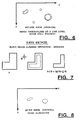
- a sub-area of DUT 10 is plotted in the XY plane with sub-area noise and defect bright spot intensities plotted on a gray level scale along the Z axis. If this micro difference image is filtered according to the prior art technique of thresholding, as shown in Figure 5, intense noise spots will pass while weak bright spots are blocked. However, the inventors of the present invention have realized that the interesting defect bright spots, whatever their intensity, characteristically extend over a certain minimum area or have other spacial characteristics, and that this characteristic may be used for a second processing step of improved filtering.
- Second stage processing is based on the image algebra operation of "erosion" as illustrated in Figure 7 in which the input image A is depicted as a solid line while the transformed image is shown by a dashed line. This allows the first stage threshold to be lowered to pass weak defect bright spots, while intense but small area noise spots are removed.
- the erosion or sieve processing removes noise from the Figure 6 image to produce an image without noise as shown in Figure 8.
- the above explained technique of erosion is not the only technique of removing random noise points which may be used.
- Other techniques are explained in the book “Algorithms for Graphics and Image Processing” by Theo Pavidis, published by the Computer Science Press, Rockville, MD (1982).
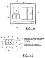
- micro difference image processing may also use context discrimination by superimposing the micro difference image onto a copy of the reflected image, as shown in Figure 9. This allows areas of the die which are not suspected of having defects, or which are outside the circuit altogether, to be identified and eliminated from suspicion of having defects.
- the present invention also provides a "paint" capability which allows a system operator who recognizes a defect bright spot pattern to circumscribe it with a rectangle, elipse, circle, or other contour, and then fill or "paint” in the contour around the defect, and thereby force the computer 14 to treat the painted area as having passed the first and second stage filters and been recognized normally (by the system).
- Use of the paint feature is automatically noted as “retouched” by computer 14 on the processed micro difference image output by the system, so that the painted-in patterns will not later be mistaken for normally identified patterns.
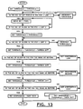
- the difference image processing algorithm (preferably as shown in the flow chart of Figure 13) operates with adjustable parameters for noise and defect bright spot gray level sensitivities and confidence margins.
- computer 14 can automatically replace the macro optic system 30 with the micro optic system 40, move stage 9 so that the first one of the recognized bright spots is in the axis of the micro optic system 30 and camera 13, and execute the image formation, differencing, and processing steps, with selectable confidence levels, according to the Figure 13 algorithm.
- Each "processed micro difference image” is superimposed onto the reflected image of the same area.
- the reflected image was received through noise-amplifying intensifier 12 and primary camera 13 and converted into digital form for storage, the retrieved reflected image may be of unsatisfactory quality for the operator to use in correlating defect locations to coordinates of the integrated circuit.
- the present invention also provides an auxiliary camera system 21 as shown in Figure 2.
- the prior art design did not appreciate that the primary camera 13 has inadequate resolution for small features, and merges groups of features if they are small in size.
- the auxiliary camera 21 is an ordinary high resolution video camera, without an image intensifier, which provides higher quality images, comparable to microscope eye piece images, side-by-side with the processed image on display 15 for the operator to better distinguish features.
- the processed micro difference image may also be compared against a reflected image of a corresponding second device under test 26, Figure 2.
- the processed difference image may be compared against the stored image of another integrated circuit of the same type known to be free of defects.
- image computer 14 may be provided with an interface to a computer aided design (CAD) system 125, Figure 11, through which the emission microscopy system under manual or automatic control can retrieve the composite layout image of each area of the integrated circuit.
- CAD computer aided design
- the invention also preferably includes means for the processed difference and superimposed macro and micro images of each area to be output to alternate display devices including a hard disk 126, a floppy disk 126, or a video image printer 128, Figure 11.
- the interior chamber illumination level is also preferably automatically controlled by computer 14 to produce good images regardless of variations in reflectivity of various DUTS.
- the preferred embodiment is operated with commands input conveniently by a "mouse and menue" operator interface system.
- This system provides process and reliability engineers with evidence of process and/or structure induced oxide failures as well as several other types of dielectrical failures and thereby helps increase device yield and reliability.
Priority Applications (1)
| Application Number | Priority Date | Filing Date | Title |
|---|---|---|---|
| AT88106874T ATE71736T1 (de) | 1987-08-31 | 1988-04-29 | Emissionsmikroskopie-geraet und -methode. |
Applications Claiming Priority (2)
| Application Number | Priority Date | Filing Date | Title |
|---|---|---|---|
| US91682 | 1987-08-31 | ||
| US07/091,682 US4755874A (en) | 1987-08-31 | 1987-08-31 | Emission microscopy system |
Publications (3)
| Publication Number | Publication Date |
|---|---|
| EP0305644A2 true EP0305644A2 (de) | 1989-03-08 |
| EP0305644A3 EP0305644A3 (en) | 1989-12-06 |
| EP0305644B1 EP0305644B1 (de) | 1992-01-15 |
Family
ID=22229122
Family Applications (1)
| Application Number | Title | Priority Date | Filing Date |
|---|---|---|---|
| EP88106874A Expired - Lifetime EP0305644B1 (de) | 1987-08-31 | 1988-04-29 | Emissionsmikroskopie-Gerät und -Methode |
Country Status (5)
| Country | Link |
|---|---|
| US (1) | US4755874A (de) |
| EP (1) | EP0305644B1 (de) |
| JP (1) | JPH0760846B2 (de) |
| AT (1) | ATE71736T1 (de) |
| DE (1) | DE3867766D1 (de) |
Cited By (6)
| Publication number | Priority date | Publication date | Assignee | Title |
|---|---|---|---|---|
| EP0453239A1 (de) * | 1990-04-16 | 1991-10-23 | Olympus Optical Co., Ltd. | Optisches Mikroskop mit variabler Vergrösserung |
| EP0510887A2 (de) * | 1991-04-26 | 1992-10-28 | Sharp Kabushiki Kaisha | Verfahren und Vorrichtung zum Erfassen und Analysieren defekter Halbleiterelemente |
| EP0741302A2 (de) * | 1995-05-03 | 1996-11-06 | Sun Microsystems, Inc. | Auslöseimpulsgenerator für die CMOS-Latch-up-Analyse |
| GB2389178A (en) * | 2001-12-31 | 2003-12-03 | Orbotech Ltd | Method for inspecting patterns |
| US7498557B2 (en) | 2005-09-08 | 2009-03-03 | Applied Materials Israel Ltd. | Cascaded image intensifier |
| WO2013189118A1 (zh) * | 2012-06-21 | 2013-12-27 | 爱威科技股份有限公司 | 图像处理方法和装置 |
Families Citing this family (96)
| Publication number | Priority date | Publication date | Assignee | Title |
|---|---|---|---|---|
| US5030829A (en) * | 1988-06-08 | 1991-07-09 | Siemens Aktiengesellschaft | Method and apparatus for investigating latch-up propagation in complementary-metal-oxide-semiconductor (CMOS) circuits |
| US5012100A (en) * | 1988-06-08 | 1991-04-30 | Siemens Aktiengesellschaft | Method and apparatus for investigating the latch-up propagation in complementary-metal-oxide semiconductor (CMOS) circuits |
| FR2636487A1 (fr) * | 1988-09-13 | 1990-03-16 | Labo Electronique Physique | Systeme de traitement d'images |
| US5006717A (en) * | 1988-12-26 | 1991-04-09 | Matsushita Electric Industrial Co., Ltd. | Method of evaluating a semiconductor device and an apparatus for performing the same |
| US5136373A (en) * | 1989-06-22 | 1992-08-04 | Hamamatsu Photonics K. K. | Image processing apparatus |
| US5270655A (en) * | 1989-12-22 | 1993-12-14 | Matsushita Electric Industrial Co., Ltd. | Semiconductor integrated circuit having light emitting devices |
| US5287183A (en) * | 1990-03-05 | 1994-02-15 | Wayne State University | Synchronous imaging system |
| JPH0479343A (ja) * | 1990-07-23 | 1992-03-12 | Nippon Telegr & Teleph Corp <Ntt> | 半導体集積回路の解析方法および解析装置 |
| US5032727A (en) * | 1990-09-14 | 1991-07-16 | Digital Equipment Corporation | Product defect detection using thermal ratio analysis |
| US5204910A (en) * | 1991-05-24 | 1993-04-20 | Motorola, Inc. | Method for detection of defects lacking distinct edges |
| US5504431A (en) * | 1991-12-09 | 1996-04-02 | Matsushita Electric Industrial Co., Ltd. | Device for and method of evaluating semiconductor integrated circuit |
| US5301006A (en) * | 1992-01-28 | 1994-04-05 | Advanced Micro Devices, Inc. | Emission microscope |
| DE69328323D1 (de) * | 1992-01-29 | 2000-05-18 | Advanced Micro Devices Inc | Energieauflösendes Emissions-Mikroskop-System und Verfahren |
| US6002792A (en) * | 1993-11-16 | 1999-12-14 | Hamamatsu Photonics Kk | Semiconductor device inspection system |
| US5475316A (en) * | 1993-12-27 | 1995-12-12 | Hypervision, Inc. | Transportable image emission microscope |
| WO1996021160A1 (en) * | 1993-12-27 | 1996-07-11 | Hypervision, Inc. | Transportable image emission microscope |
| US5557097A (en) * | 1994-09-20 | 1996-09-17 | Neopath, Inc. | Cytological system autofocus integrity checking apparatus |
| US5668660A (en) * | 1994-11-29 | 1997-09-16 | Hunt; Gary D. | Microscope with plural zoom lens assemblies in series |
| US5500770A (en) * | 1994-12-30 | 1996-03-19 | Amarel Precision Instruments | Macrolens system for emission microscopy |
| US5724131A (en) * | 1995-06-14 | 1998-03-03 | The National University Of Singapore | Integrated emission microscope for panchromatic imaging, continuous wavelength spectroscopy and selective area spectroscopic mapping |
| US5970167A (en) * | 1995-11-08 | 1999-10-19 | Alpha Innotech Corporation | Integrated circuit failure analysis using color voltage contrast |
| US5892539A (en) * | 1995-11-08 | 1999-04-06 | Alpha Innotech Corporation | Portable emission microscope workstation for failure analysis |
| US6078681A (en) * | 1996-03-18 | 2000-06-20 | Marine Biological Laboratory | Analytical imaging system and process |
| US6259827B1 (en) * | 1996-03-21 | 2001-07-10 | Cognex Corporation | Machine vision methods for enhancing the contrast between an object and its background using multiple on-axis images |
| US5764409A (en) * | 1996-04-26 | 1998-06-09 | Alpha Innotech Corp | Elimination of vibration by vibration coupling in microscopy applications |
| US5940545A (en) * | 1996-07-18 | 1999-08-17 | International Business Machines Corporation | Noninvasive optical method for measuring internal switching and other dynamic parameters of CMOS circuits |
| US5914613A (en) | 1996-08-08 | 1999-06-22 | Cascade Microtech, Inc. | Membrane probing system with local contact scrub |
| US5754291A (en) * | 1996-09-19 | 1998-05-19 | Molecular Dynamics, Inc. | Micro-imaging system |
| EP0853243A3 (de) * | 1997-01-13 | 1999-07-28 | Schlumberger Technologies, Inc. | Verfahren und Vorrichtung für die Wafer-Fehlerdetektion |
| US5783835A (en) * | 1997-03-17 | 1998-07-21 | Probing Solutions, Incorporated | Probing with backside emission microscopy |
| SG66376A1 (en) * | 1997-07-03 | 1999-07-20 | Inst Of Microlectronics Nation | Multiwavelength imaging and spectroscopic photoemission microscope system |
| US5959461A (en) * | 1997-07-14 | 1999-09-28 | Wentworth Laboratories, Inc. | Probe station adapter for backside emission inspection |
| US6650768B1 (en) * | 1998-02-19 | 2003-11-18 | International Business Machines Corporation | Using time resolved light emission from VLSI circuit devices for navigation on complex systems |
| US6172512B1 (en) * | 1998-02-19 | 2001-01-09 | International Business Machines Corporation | Image processing methods for the optical detection of dynamic errors in integrated circuits |
| JP2002505436A (ja) * | 1998-02-25 | 2002-02-19 | エム.シェパード スティーヴン | 物質の非破壊評価のためのデータ統合と登録方法 |
| US6107107A (en) * | 1998-03-31 | 2000-08-22 | Advanced Micro Devices, Inc. | Analyzing an electronic circuit formed upon a frontside surface of a semiconductor substrate by detecting radiation exiting a backside surface coated with an antireflective material |
| US6256882B1 (en) | 1998-07-14 | 2001-07-10 | Cascade Microtech, Inc. | Membrane probing system |
| US6327394B1 (en) | 1998-07-21 | 2001-12-04 | International Business Machines Corporation | Apparatus and method for deriving temporal delays in integrated circuits |
| US6529018B1 (en) | 1998-08-28 | 2003-03-04 | International Business Machines Corporation | Method for monitoring defects in polysilicon gates in semiconductor devices responsive to illumination by incident light |
| US6445202B1 (en) | 1999-06-30 | 2002-09-03 | Cascade Microtech, Inc. | Probe station thermal chuck with shielding for capacitive current |
| US6650130B1 (en) | 1999-08-31 | 2003-11-18 | International Business Machines Corporation | Integrated circuit device defect detection method and apparatus employing light emission imaging |
| US6642955B1 (en) * | 2000-01-10 | 2003-11-04 | Extreme Cctv Inc. | Surveillance camera system with infrared and visible light bandpass control circuit |
| US6914423B2 (en) | 2000-09-05 | 2005-07-05 | Cascade Microtech, Inc. | Probe station |
| US6965226B2 (en) | 2000-09-05 | 2005-11-15 | Cascade Microtech, Inc. | Chuck for holding a device under test |
| US6469536B1 (en) * | 2000-10-17 | 2002-10-22 | Motorola, Inc. | Method and device for providing symetrical monitoring of ESD testing an integrated circuit |
| US6633173B1 (en) * | 2000-10-24 | 2003-10-14 | Renesas Technology America, Inc | Method and apparatus for testing for latch-up in integrated circuits |
| KR100383258B1 (ko) * | 2000-11-09 | 2003-05-09 | 삼성전자주식회사 | 주사 전자 현미경을 이용한 측정 장치의 측정 에러 검출방법 |
| DE20114544U1 (de) | 2000-12-04 | 2002-02-21 | Cascade Microtech Inc | Wafersonde |
| US20020150294A1 (en) * | 2001-02-02 | 2002-10-17 | Honeywell Federal Manufacturing & Technologies, Llc | Automated imaging system and method for concrete quality analysis |
| JPWO2002067039A1 (ja) * | 2001-02-19 | 2004-06-24 | オリンパス株式会社 | 画像比較装置、画像比較方法及び画像比較をコンピュータに実行させるプログラム |
| US6716683B1 (en) * | 2001-06-22 | 2004-04-06 | Advanced Mircor Devices, Inc. | Optical analysis for SOI integrated circuits |
| US6850081B1 (en) * | 2001-07-26 | 2005-02-01 | Advanced Micro Devices, Inc. | Semiconductor die analysis via fiber optic communication |
| WO2003052435A1 (en) | 2001-08-21 | 2003-06-26 | Cascade Microtech, Inc. | Membrane probing system |
| US6621275B2 (en) | 2001-11-28 | 2003-09-16 | Optonics Inc. | Time resolved non-invasive diagnostics system |
| KR20040103918A (ko) * | 2002-01-23 | 2004-12-09 | 마리나 시스템 코포레이션 | 결함 검출 및 분석을 위한 적외선 서모그래피 |
| US7538815B1 (en) | 2002-01-23 | 2009-05-26 | Marena Systems Corporation | Autofocus system and method using focus measure gradient |
| CA2492416A1 (en) * | 2002-07-15 | 2004-01-22 | Baylor College Of Medicine | Computer user interface facilitating acquiring and analyzing of biological specimen traits |
| US6788093B2 (en) * | 2002-08-07 | 2004-09-07 | International Business Machines Corporation | Methodology and apparatus using real-time optical signal for wafer-level device dielectrical reliability studies |
| US7315324B2 (en) * | 2002-08-15 | 2008-01-01 | Dixon Cleveland | Motion clutter suppression for image-subtracting cameras |
| US6943572B2 (en) * | 2002-09-03 | 2005-09-13 | Credence Systems Corporation | Apparatus and method for detecting photon emissions from transistors |
| US6891363B2 (en) * | 2002-09-03 | 2005-05-10 | Credence Systems Corporation | Apparatus and method for detecting photon emissions from transistors |
| TWI239063B (en) * | 2002-12-20 | 2005-09-01 | Delta Electronics Inc | Method for detecting defectives in an integrated circuit |
| US7492172B2 (en) | 2003-05-23 | 2009-02-17 | Cascade Microtech, Inc. | Chuck for holding a device under test |
| US7057404B2 (en) | 2003-05-23 | 2006-06-06 | Sharp Laboratories Of America, Inc. | Shielded probe for testing a device under test |
| US7245758B2 (en) * | 2003-08-20 | 2007-07-17 | Lsi Corporation | Whole-wafer photoemission analysis |
| US7256055B2 (en) * | 2003-08-25 | 2007-08-14 | Tau-Metrix, Inc. | System and apparatus for using test structures inside of a chip during the fabrication of the chip |
| US7250626B2 (en) | 2003-10-22 | 2007-07-31 | Cascade Microtech, Inc. | Probe testing structure |
| DE202004021093U1 (de) | 2003-12-24 | 2006-09-28 | Cascade Microtech, Inc., Beaverton | Aktiver Halbleiterscheibenmessfühler |
| US7187188B2 (en) | 2003-12-24 | 2007-03-06 | Cascade Microtech, Inc. | Chuck with integrated wafer support |
| US7420381B2 (en) | 2004-09-13 | 2008-09-02 | Cascade Microtech, Inc. | Double sided probing structures |
| US7656172B2 (en) | 2005-01-31 | 2010-02-02 | Cascade Microtech, Inc. | System for testing semiconductors |
| US7535247B2 (en) | 2005-01-31 | 2009-05-19 | Cascade Microtech, Inc. | Interface for testing semiconductors |
| CN100573168C (zh) * | 2005-04-21 | 2009-12-23 | 鸿富锦精密工业(深圳)有限公司 | 测试计算机面板发光二极管灯及其连接线的系统及方法 |
| US20070051879A1 (en) * | 2005-09-08 | 2007-03-08 | Tal Kuzniz | Image Intensifier Device and Method |
| US20070124628A1 (en) * | 2005-11-30 | 2007-05-31 | Lsi Logic Corporation | Methods of memory bitmap verification for finished product |
| US7403028B2 (en) | 2006-06-12 | 2008-07-22 | Cascade Microtech, Inc. | Test structure and probe for differential signals |
| US7723999B2 (en) | 2006-06-12 | 2010-05-25 | Cascade Microtech, Inc. | Calibration structures for differential signal probing |
| US7764072B2 (en) | 2006-06-12 | 2010-07-27 | Cascade Microtech, Inc. | Differential signal probing system |
| US20080145040A1 (en) * | 2006-12-19 | 2008-06-19 | Cytyc Corporation | Simultaneous imaging of multiple specimen slides on a single slide stage |
| US7876114B2 (en) | 2007-08-08 | 2011-01-25 | Cascade Microtech, Inc. | Differential waveguide probe |
| JP2009139155A (ja) * | 2007-12-04 | 2009-06-25 | Ueno Seiki Kk | 検査システム、画像検査装置及びその制御方法 |
| US7888957B2 (en) | 2008-10-06 | 2011-02-15 | Cascade Microtech, Inc. | Probing apparatus with impedance optimized interface |
| US8410806B2 (en) | 2008-11-21 | 2013-04-02 | Cascade Microtech, Inc. | Replaceable coupon for a probing apparatus |
| US8319503B2 (en) | 2008-11-24 | 2012-11-27 | Cascade Microtech, Inc. | Test apparatus for measuring a characteristic of a device under test |
| US8319501B2 (en) * | 2009-06-22 | 2012-11-27 | Xerox Corporation | Optical component identifier |
| US8331726B2 (en) * | 2009-06-29 | 2012-12-11 | International Business Machines Corporation | Creating emission images of integrated circuits |
| US8472736B2 (en) * | 2010-09-30 | 2013-06-25 | The Charles Stark Draper Laboratory, Inc. | Attitude estimation by reducing noise with dragback |
| US8472737B2 (en) | 2010-09-30 | 2013-06-25 | The Charles Stark Draper Laboratory, Inc. | Attitude estimation in compressed domain |
| US8472735B2 (en) | 2010-09-30 | 2013-06-25 | The Charles Stark Draper Laboratory, Inc. | Attitude estimation with compressive sampling of starfield data |
| US9494856B1 (en) | 2011-06-07 | 2016-11-15 | Hermes Microvision, Inc. | Method and system for fast inspecting defects |
| US9557369B2 (en) | 2012-06-22 | 2017-01-31 | International Business Machines Corporation | Integrated time dependent dielectric breakdown reliability testing |
| US10514418B2 (en) * | 2013-04-10 | 2019-12-24 | Fei Company | Optimized wavelength photon emission microscope for VLSI devices |
| TWI500927B (zh) * | 2013-10-14 | 2015-09-21 | Nat Univ Tsing Hua | 非接觸式中介層檢測方法與裝置 |
| JP2017073548A (ja) * | 2015-10-05 | 2017-04-13 | エフイーアイ カンパニー | Vlsi装置用の最適波長光子放射顕微鏡 [関連出願の参照] 本出願は、2015年10月5日に出願された米国仮出願第62/237,399号の優先権利益を主張し、そのすべての内容が本明細書に参考として援用される。[政府許認可権] 本発明は、空軍研究所(afrl)の契約番号fa8650−11−c−7105を介した、アメリカ合衆国国家情報長官官房(odni)、情報先端研究プロジェクト活動(iarpa)による支援事業に基づくものである。本明細書に含まれるアイデア及び結果は、本発明者らのアイデア及び結果であり、odni、iarpa、afrl又は米国政府の公式承認を必ずしも有するものとして解釈されるべきでない。 |
| CN107179494B (zh) * | 2017-05-27 | 2023-06-09 | 浙江万里学院 | 一种通用电路板板上器件故障检测方法及系统 |
| US11543639B2 (en) * | 2019-01-29 | 2023-01-03 | Li-Cor, Inc. | Macro-micro telecentric scanning systems and methods |
Citations (3)
| Publication number | Priority date | Publication date | Assignee | Title |
|---|---|---|---|---|
| DE2450526A1 (de) * | 1973-10-30 | 1975-05-07 | Westinghouse Electric Corp | Verfahren zur pruefung eines koerpers vorgegebenen schaltungsaufbaus |
| US4389669A (en) * | 1981-02-27 | 1983-06-21 | Ilc Data Device Corporation | Opto-video inspection system |
| US4680635A (en) * | 1986-04-01 | 1987-07-14 | Intel Corporation | Emission microscope |
-
1987
- 1987-08-31 US US07/091,682 patent/US4755874A/en not_active Expired - Lifetime
-
1988
- 1988-04-29 DE DE8888106874T patent/DE3867766D1/de not_active Expired - Fee Related
- 1988-04-29 EP EP88106874A patent/EP0305644B1/de not_active Expired - Lifetime
- 1988-04-29 AT AT88106874T patent/ATE71736T1/de not_active IP Right Cessation
- 1988-06-20 JP JP63150385A patent/JPH0760846B2/ja not_active Expired - Lifetime
Patent Citations (3)
| Publication number | Priority date | Publication date | Assignee | Title |
|---|---|---|---|---|
| DE2450526A1 (de) * | 1973-10-30 | 1975-05-07 | Westinghouse Electric Corp | Verfahren zur pruefung eines koerpers vorgegebenen schaltungsaufbaus |
| US4389669A (en) * | 1981-02-27 | 1983-06-21 | Ilc Data Device Corporation | Opto-video inspection system |
| US4680635A (en) * | 1986-04-01 | 1987-07-14 | Intel Corporation | Emission microscope |
Non-Patent Citations (2)
| Title |
|---|
| SOLID STATE TECHNOLOGY * |
| SOLIDE STATE TECHNOLOGY February 1984, pages 159-179; K. L. Harris et al.: "Automated Inspection of Wafer Patterns with Applications in Stepping, Projection and Direct-Write Lithography" abstract; page 161, left column, paragraphes 3-5; figure 2 * |
Cited By (11)
| Publication number | Priority date | Publication date | Assignee | Title |
|---|---|---|---|---|
| EP0453239A1 (de) * | 1990-04-16 | 1991-10-23 | Olympus Optical Co., Ltd. | Optisches Mikroskop mit variabler Vergrösserung |
| US5276550A (en) * | 1990-04-16 | 1994-01-04 | Olympus Optical Co., Ltd. | Optical microscope with variable magnification |
| EP0510887A2 (de) * | 1991-04-26 | 1992-10-28 | Sharp Kabushiki Kaisha | Verfahren und Vorrichtung zum Erfassen und Analysieren defekter Halbleiterelemente |
| EP0510887A3 (en) * | 1991-04-26 | 1993-02-24 | Sharp Kabushiki Kaisha | Method and apparatus for detecting and analyzing defective semiconductor element |
| US5391885A (en) * | 1991-04-26 | 1995-02-21 | Sharp Kabushiki Kaisha | Method of detecting and analyzing defective portion of semiconductor element and apparatus for detecting and analyzing the same |
| EP0741302A2 (de) * | 1995-05-03 | 1996-11-06 | Sun Microsystems, Inc. | Auslöseimpulsgenerator für die CMOS-Latch-up-Analyse |
| EP0741302A3 (de) * | 1995-05-03 | 1996-11-20 | Sun Microsystems, Inc. | Auslöseimpulsgenerator für die CMOS-Latch-up-Analyse |
| GB2389178A (en) * | 2001-12-31 | 2003-12-03 | Orbotech Ltd | Method for inspecting patterns |
| GB2389178B (en) * | 2001-12-31 | 2004-10-27 | Orbotech Ltd | Method for inspecting patterns |
| US7498557B2 (en) | 2005-09-08 | 2009-03-03 | Applied Materials Israel Ltd. | Cascaded image intensifier |
| WO2013189118A1 (zh) * | 2012-06-21 | 2013-12-27 | 爱威科技股份有限公司 | 图像处理方法和装置 |
Also Published As
| Publication number | Publication date |
|---|---|
| JPS6472540A (en) | 1989-03-17 |
| DE3867766D1 (de) | 1992-02-27 |
| US4755874A (en) | 1988-07-05 |
| ATE71736T1 (de) | 1992-02-15 |
| EP0305644A3 (en) | 1989-12-06 |
| JPH0760846B2 (ja) | 1995-06-28 |
| EP0305644B1 (de) | 1992-01-15 |
Similar Documents
| Publication | Publication Date | Title |
|---|---|---|
| US4755874A (en) | Emission microscopy system | |
| US6198529B1 (en) | Automated inspection system for metallic surfaces | |
| EP0713593B1 (de) | Verfahren und gerät für ein lötkugelkontrollsystem | |
| JP4035974B2 (ja) | 欠陥観察方法及びその装置 | |
| US5892539A (en) | Portable emission microscope workstation for failure analysis | |
| US7242015B2 (en) | Patterned wafer inspection method and apparatus therefor | |
| US6175646B1 (en) | Apparatus for detecting defective integrated circuit dies in wafer form | |
| JP4183492B2 (ja) | 欠陥検査装置および欠陥検査方法 | |
| KR100775437B1 (ko) | 패턴검사장치및그방법 | |
| US8581976B2 (en) | Method and apparatus for reviewing defects of semiconductor device | |
| US5475316A (en) | Transportable image emission microscope | |
| US7626163B2 (en) | Defect review method and device for semiconductor device | |
| US7105815B2 (en) | Method and apparatus for collecting defect images | |
| KR20070012554A (ko) | 주문형 자동 광학 검사 서브 시스템을 이용하는 티에프티엘씨디 패널의 개선된 검사 | |
| US6553323B1 (en) | Method and its apparatus for inspecting a specimen | |
| WO2000057162A2 (en) | Optical inspection of semi-conductor structures | |
| JP2000030652A (ja) | 試料の観察方法およびその装置 | |
| EP0510887B1 (de) | Verfahren zum Erfassen und Analysieren defekter Halbleiterelemente | |
| JP2004031379A (ja) | 電子線を用いた検査方法及び検査装置 | |
| JP2000346627A (ja) | 検査装置 | |
| JP3665194B2 (ja) | 回路パターンの検査方法及び検査装置 | |
| JP2904642B2 (ja) | 半導体素子不良箇所検出方法 | |
| JP2005101619A (ja) | パターン欠陥検査方法および検査装置 | |
| JP2008147679A (ja) | 電子線応用装置 | |
| WO1996021160A1 (en) | Transportable image emission microscope |
Legal Events
| Date | Code | Title | Description |
|---|---|---|---|
| PUAI | Public reference made under article 153(3) epc to a published international application that has entered the european phase |
Free format text: ORIGINAL CODE: 0009012 |
|
| AK | Designated contracting states |
Kind code of ref document: A2 Designated state(s): AT BE CH DE ES FR GB GR IT LI LU NL SE |
|
| PUAL | Search report despatched |
Free format text: ORIGINAL CODE: 0009013 |
|
| AK | Designated contracting states |
Kind code of ref document: A3 Designated state(s): AT BE CH DE ES FR GB GR IT LI LU NL SE |
|
| RHK1 | Main classification (correction) |
Ipc: G01R 31/28 |
|
| 17P | Request for examination filed |
Effective date: 19900210 |
|
| 17Q | First examination report despatched |
Effective date: 19900426 |
|
| GRAA | (expected) grant |
Free format text: ORIGINAL CODE: 0009210 |
|
| AK | Designated contracting states |
Kind code of ref document: B1 Designated state(s): AT BE CH DE ES FR GB GR IT LI LU NL SE |
|
| PG25 | Lapsed in a contracting state [announced via postgrant information from national office to epo] |
Ref country code: BE Effective date: 19920115 Ref country code: AT Effective date: 19920115 Ref country code: ES Free format text: THE PATENT HAS BEEN ANNULLED BY A DECISION OF A NATIONAL AUTHORITY Effective date: 19920115 Ref country code: LI Effective date: 19920115 Ref country code: GR Free format text: LAPSE BECAUSE OF FAILURE TO SUBMIT A TRANSLATION OF THE DESCRIPTION OR TO PAY THE FEE WITHIN THE PRESCRIBED TIME-LIMIT Effective date: 19920115 Ref country code: NL Effective date: 19920115 Ref country code: CH Effective date: 19920115 Ref country code: SE Effective date: 19920115 Ref country code: IT Free format text: LAPSE BECAUSE OF FAILURE TO SUBMIT A TRANSLATION OF THE DESCRIPTION OR TO PAY THE FEE WITHIN THE PRESCRIBED TIME-LIMIT;WARNING: LAPSES OF ITALIAN PATENTS WITH EFFECTIVE DATE BEFORE 2007 MAY HAVE OCCURRED AT ANY TIME BEFORE 2007. THE CORRECT EFFECTIVE DATE MAY BE DIFFERENT FROM THE ONE RECORDED. Effective date: 19920115 |
|
| REF | Corresponds to: |
Ref document number: 71736 Country of ref document: AT Date of ref document: 19920215 Kind code of ref document: T |
|
| REF | Corresponds to: |
Ref document number: 3867766 Country of ref document: DE Date of ref document: 19920227 |
|
| PG25 | Lapsed in a contracting state [announced via postgrant information from national office to epo] |
Ref country code: LU Free format text: LAPSE BECAUSE OF NON-PAYMENT OF DUE FEES Effective date: 19920430 |
|
| REG | Reference to a national code |
Ref country code: CH Ref legal event code: PL |
|
| ET | Fr: translation filed | ||
| NLV1 | Nl: lapsed or annulled due to failure to fulfill the requirements of art. 29p and 29m of the patents act | ||
| PLBE | No opposition filed within time limit |
Free format text: ORIGINAL CODE: 0009261 |
|
| STAA | Information on the status of an ep patent application or granted ep patent |
Free format text: STATUS: NO OPPOSITION FILED WITHIN TIME LIMIT |
|
| 26N | No opposition filed | ||
| REG | Reference to a national code |
Ref country code: GB Ref legal event code: 732E |
|
| REG | Reference to a national code |
Ref country code: FR Ref legal event code: TP |
|
| PGFP | Annual fee paid to national office [announced via postgrant information from national office to epo] |
Ref country code: GB Payment date: 19970324 Year of fee payment: 10 |
|
| PGFP | Annual fee paid to national office [announced via postgrant information from national office to epo] |
Ref country code: FR Payment date: 19970328 Year of fee payment: 10 |
|
| PGFP | Annual fee paid to national office [announced via postgrant information from national office to epo] |
Ref country code: DE Payment date: 19970618 Year of fee payment: 10 |
|
| PG25 | Lapsed in a contracting state [announced via postgrant information from national office to epo] |
Ref country code: GB Free format text: LAPSE BECAUSE OF NON-PAYMENT OF DUE FEES Effective date: 19980429 |
|
| PG25 | Lapsed in a contracting state [announced via postgrant information from national office to epo] |
Ref country code: FR Free format text: THE PATENT HAS BEEN ANNULLED BY A DECISION OF A NATIONAL AUTHORITY Effective date: 19980430 |
|
| GBPC | Gb: european patent ceased through non-payment of renewal fee |
Effective date: 19980429 |
|
| PG25 | Lapsed in a contracting state [announced via postgrant information from national office to epo] |
Ref country code: DE Free format text: LAPSE BECAUSE OF NON-PAYMENT OF DUE FEES Effective date: 19990202 |
|
| REG | Reference to a national code |
Ref country code: FR Ref legal event code: ST |
|
| P01 | Opt-out of the competence of the unified patent court (upc) registered |
Effective date: 20230525 |