EP0741302A2 - Auslöseimpulsgenerator für die CMOS-Latch-up-Analyse - Google Patents
Auslöseimpulsgenerator für die CMOS-Latch-up-Analyse Download PDFInfo
- Publication number
- EP0741302A2 EP0741302A2 EP96302941A EP96302941A EP0741302A2 EP 0741302 A2 EP0741302 A2 EP 0741302A2 EP 96302941 A EP96302941 A EP 96302941A EP 96302941 A EP96302941 A EP 96302941A EP 0741302 A2 EP0741302 A2 EP 0741302A2
- Authority
- EP
- European Patent Office
- Prior art keywords
- internal
- pulse
- output
- pulse signal
- pulse train
- Prior art date
- Legal status (The legal status is an assumption and is not a legal conclusion. Google has not performed a legal analysis and makes no representation as to the accuracy of the status listed.)
- Withdrawn
Links
Images


Classifications
-
- G—PHYSICS
- G01—MEASURING; TESTING
- G01R—MEASURING ELECTRIC VARIABLES; MEASURING MAGNETIC VARIABLES
- G01R31/00—Arrangements for testing electric properties; Arrangements for locating electric faults; Arrangements for electrical testing characterised by what is being tested not provided for elsewhere
- G01R31/28—Testing of electronic circuits, e.g. by signal tracer
- G01R31/2851—Testing of integrated circuits [IC]
- G01R31/2853—Electrical testing of internal connections or -isolation, e.g. latch-up or chip-to-lead connections
Definitions
- the present invention relates generally to failure analysis of complementary-metal-oxide-semiconductor ("CMOS”) transistors, and more particularly to equipment for analysis of latch-up failure in CMOS integrated circuits.
- CMOS complementary-metal-oxide-semiconductor
- CMOS transistors Integrated circuits fabricated with CMOS transistors advantageously consume little DC current and are readily produced. Unfortunately, however, CMOS transistors are susceptible to a phenomenon known as "latch-up".
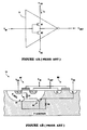
- Figure 1A depicts a generic CMOS inverter 10 coupled between the upper and lower power supplies, VDD and VSS.
- the inverter includes a P-type or PMOS transistor M1 and an N-type or NMOS transistor M2.
- the gates of M1 and M2 are coupled together to an input port that receives a V IN signal, and the source of M1 and the drain of M2 are coupled together to an output port that provides a V OUT signal that is an inversion of VIN.
- the drain of M1 is coupled to VDD and the source of M2 is coupled to VSS, which is commonly ground.
- VOUT is an inverted version of VIN, and under DC or static conditions, essentially no dissipation within the transistors occurs since when M1 is turned on, M2 is turned off, and vice versa.
- the current i o provided by the upper power supply V DD typically is limited to approximately V DD /R L , where R L is the resistive component of the load being driven by inverter 10.
- FIG. 1B is a simplified cross-section of a P-type substrate upon which inverter 10 has been fabricated.
- PMOS transistor M1 is fabricated with an N well and includes two spaced-apart P+ regions that define M1's source and drain, and a gate that overlies and is separated from the spaced-apart region by a thin oxide layer.
- NMOS transistor M2 includes two spaced-apart N+ regions that define M2's source and drain, and a gate that overlies and is separated from the spaced-apart region by a thin oxide layer.
- M1's P+ drain region is coupled to VDD
- M1's P+ source region is coupled to VOUT and to M2's N+ drain region
- the gates of M1 and M2 are coupled together to receive a VIN signal
- M2's N+ source region is coupled to the lower power supply VSS.
- PNP bipolar transistor Q1 is defined by a P+ doped emitter region (e.g., the P+ drain of M1), an N doped base region (e.g., the N well containing PMOS transistor M1), and a P doped collector region (e.g., the P substrate).
- NPN bipolar transistor Q2 is defined by an N doped collector region (e.g., the N well containing PMOS transistor M1), and P doped base region (e.g., the P substrate), and an N doped emitter region (e.g., the N+ source of NMOS transistor M2).
- conductive paths may exist defining resistors R1 and R2, respectively coupled across Q1's emitter-base junction, and across Q2's emitter base junction.
- Latch-up current from VDD through Q1, Q2 to VSS can readily reach an ampere or so, within a few hundred nanoseconds or less. As such, latch-up current is far in excess of the nominal load current i o associated with inverter 10. The resultant high latch-up current flow and attendant heat can damage or destroy inverter 10 (or other CMOS circuit) before it is even known to interrupt the power supply. Of course, in actual applications, interrupting operating power to inverter 10 will also interrupt operating power to many other ICs as well, further hampering performance of the system containing the ICs.
- inverter CMOS circuits such as inverter 10
- inverter 10 it is known to reduce latch-up by keeping the current gain ⁇ for bipolar transistors Q1 and Q2 low, and by keeping the bulk resistance of the substrate high.
- the rapidity with which latch-up destruction can occur hampers the analysis procedure.
- the inverter of Figure 1A is but one example of a CMOS-implemented circuit that is susceptible to latch-up.
- non-inverter CMOS circuits can also be susceptible to such damage.
- latch-up is characterized by forward biased emitter-base junctions for the parasitic bipolar transistors Q1 and Q2. Under high current latch-up conditions, these emitter-bias junctions emit photons. These photo emissions can be examined using an emission microscope, in an attempt to analyze the latch-up problem with a view to modifying the IC layout or design to avoid future latch-up.
- a single composite pulse train is coupled to the power pin of the CMOS device under test.
- the composite pulse train has a first voltage level approximating a level of the first pulse train.
- superimposed on a portion of the first voltage level is a trigger pulse having a higher voltage level approximating the trigger pulse level of the second pulse train.
- Hamamatsu provided a system that included a dedicated digital delay and pulse generator (their model DG535), a latch-up pulse generator, and a gate controlled camera. This system output first and second pulse trains for signal pin latch-up testing, but did not provide a composite pulse for power pin testing.
- the second pulse train (the trigger pulse train) was apparently output by charging and discharging one or more capacitors. This use of capacitors had the unfortunate result that the pulse width of the trigger pulse could not readily be user controlled. The system did, however, allow variation in the delay between the trigger pulse and the first pulse train, and in the amplitude of the pulse trains.
- This system was designed for use with a Hamamatsu emission microscope whose images of a CMOS device in latch-up would be photographed in synchronism with operation of the gate controlled camera.
- the DG535 controllably output synchronization trigger pulses to the latch-up generator and to the camera control gate.
- signal-pin latch-up in the device under test could be induced, whereupon the gate controlled camera could record emission microscope images for later analysis of any latch-up.
- the Hamamatsu system was essentially dedicated for use with the gate controlled camera, and associated emission microscope.
- the system did not meet Joint Electronic Device Engineering Committee (“JEDEC”) standards, in that there was no provision for power pin latch-up testing.
- JEDEC Joint Electronic Device Engineering Committee
- signal pin testing was possible, essentially no user control over the width of the second pulse train (trigger pulse) was provided.
- the cost of the Hamamatsu apparatus was relatively high, as much as $10,000 for the SG535 digital delay generator alone.
- the system should be self-contained and permit latch-up analysis with essentially any type of emission microscope. Finally, such system should cost substantially less than several thousand dollars to implement.
- the present invention discloses such a system.
- a latch-up pulse generator system includes a latch-up pulse generator coupled to first and second power supplies, for outputting first and second output pulse trains.
- the generator includes a master clock, digital frequency dividers, and digitally switchable delay circuitry for outputting the two pulse trains.
- the system meets the newly proposed JEDEC "IC Latch-up Test" standard protocol and can test signal pins and/or power pins for a CMOS device under test. Signal pin testing uses both pulse trains, whereas power pin testing superimposes the two pulse trains to create a composite pulse train.
- the first pulse train is a square-wave signal with a repetition rate of about two seconds, an amplitude that is user adjustable from 0 VDC to perhaps 15 VDC at a current level of about 5 A.
- the second pulse train (the trigger pulse) has a pulse width that is digitally switchable between about 0.2 ⁇ s, 1.5 ⁇ s, and 5 ⁇ s.
- the delay between the fall-times of the second pulse train and the first pulse train (e.g., the time during which latch-up may be induced) is switcheably controlled between about 1 ⁇ s and 1 second, preferably in 1 ⁇ s steps.
- the amplitude and current output of the second pulse train is similarly user adjusted from 0 VDC to perhaps 15 VDC at a current level of about 5 A.
- the first and second pulse trains switch solid state relays coupled to the first and second power supplies.
- a third pulse train a composite formed by superimposing the first and second pulse trains, is used.
- the pulse width and delay associated with the second pulse train are digitally controllable. This permits a user to halt latch-up at any point in the latch-up phenomenon for purposes of observation, analysis and recordation.
- This user control allows the present invention to provide a measure of sensitivity of the device under test to latch-up.
- a generic emission microscope is used to observe the device under test. Because the latch-up phenomenon may be repeated, the emission microscope output may be photographed using conventional techniques.
- Figure 2A depicts a system for controllably creating onset and progression of signal pin latch-up in a CMOS device under test ("DUT") 10.
- the system includes the present invention 20, a latch-up trigger pulse generator, that is coupled to preferably two independent power supplies 30, 40.
- Each power supply can controllably output a DC voltage variable in amplitude A1, A2 from 0 to perhaps 15 V, at current levels of about 5 A, although other voltages and current ratings could be used.
- the system also includes a low voltage power supply, typically about 5 VDC, that powers the components comprising generator 20.
- Generator 20 outputs first and second pulse trains (PULSE 1, PULSE 2) that meet JEDEC latch-up testing standards.
- signal pin testing e.g., input pin, output pin, input/output pins
- a pulse train comprising the superposition of PULSE 1 and PULSE 2 is used.
- PULSE 1 In signal pin testing, PULSE 1 typically has set to an amplitude Al approximating the nominal operating voltage for DUT 10. For example, if DUT 10 includes CMOS transistors designed to work at 5 VDC (e.g., VDD to VSS), then amplitude Al will be set to about 5 VDC. During signal pin testing, DUT 10 receives operating potential from PULSE 1. Thus, latch-up can only occur when PULSE 1 is "high".
- Latch-up is triggered by the presence of the PULSE 2 trigger pulses, which pulses occur when PULSE 1 is high. After it begins, the latch-up phenomenon will terminate when the PULSE 1 signal returns to zero, as was described with respect to Figure 1B.
- PULSE 1 is at a "low" level, DUT 10 can cool down from the thermal heating effects of latch-up. For some CMOS devices 10 latch-up will be triggered on the rising edge of PULSE 2, and on other devices, triggering of latch-up will occur on the falling edge of PULSE 2.
- the present invention advantageously provides user control over pulse width T4, delay T5 and pulse amplitudes.
- latch-up in DUT 10 is characterized by forward biased emitter-base junctions that emit photons.
- the photon patterns preferably are examined with a conventional or generic emission microscope 50.
- microscope 50 generally includes a charge-coupled-device ("CCD") type camera for recording the emission patterns.
- CCD charge-coupled-device
- An oscilloscope 60 may also be coupled to the PULSE 1, PULSE 2 signals to aid in the use of the system, and a current probe 70 may be coupled from PULSE 1 to oscilloscope 60 as well.
- DUT 10 must be in view of the emission microscope 50.
- DUT 10 may be on a wafer, or may be a finished IC that has not undergone completion of packaging. If packaging is complete, the upper portion of the package may be removed for latch-up testing of DUT 10.
- Generator 20 preferably includes user switches or controls SW1-SW6 and SW9, permitting digital control over the pulse width T4 of PULSE 2, as well as the delay time T5 between the end of PULSE 2 and the end of PULSE 1.
- Generator 20 also includes user switches or controls SW7, SW8, and SW10 for controlling the mode of the two pulse trains, and for superimposing the pulse trains to create a composite third pulse train for power pin testing.
- Figure 2B is similar to Figure 2A except that a composite pulse train PULSE 3 is now generated by pulse generator 20, and is coupled to the power pin of the CMOS DUT 10 for power pin testing.
- the composite pulse train has a first amplitude level A1 that typically approximates the nominal operating voltage of DUT 10 (e.g., perhaps 5 VDC), and a higher second amplitude level A1+A2, of pulse width duration T4.
- Amplitude A1 is set by varying power supply 30, and amplitude A2 is set by varying power supply 40.
- power pin latch-up is triggered by the presence of the second amplitude level, A1+A2, which level has a pulse width T4. Similar to what was described above, the present invention permits the user to adjust trigger pulse width T4, delay T5, as well as amplitudes A1 and A2. The resultant flexibility allows latch-up sensitivity to be readily evaluated, again using a generic emission microscope 50.
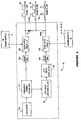
- Figure 3 is a block diagram of a preferred embodiment of generator 20, a schematic for which appears as Figure 4.
- Figure 3 also depicts one method of generating the composite power-pin testing pulse train PULSE 3.
- a master oscillator 100 preferably a generic-type crystal controlled clock oscillating at about 1 MHz, e.g., with a period T o of 1 ⁇ s, provides a precision pulse train to a digital frequency divider 110.
- frequency divider unit 110 comprises ICs denoted U1-U6 and U10.
- ICs U1-U6 are 4017-type decade counters, preferably implemented in CMOS for low power consumption.
- IC U10 is a 4040-type 12-stage binary counter.
- U1-U6 and U10 frequency divides the crystal controlled 1 MHz signal by 2,000,000 and provides a substantially 50% duty cycle square-wave whose period T1+T2 is 2.0 seconds (see Figure 2).
- substantially 50% duty cycle it is meant that the duty cycle is provided by a flip-flop whose output waveform ideally is 50%, but in practice may deviate from 50% very slightly (e.g., perhaps a few percent) in that it is impossible to realize an ideal flip-flop in practice.
- a 1.0 second "low" portion of the PULSE 1 waveform advantageously provides adequate time during which the DUT 10 can cool down from any latch-up phenomenon, before the next latch-up is induced by the trigger pulse, PULSE 2.
- ICs U10 and U8 cause PULSE 2 to have a two second, rather than one second, repetition rate since there is no need for a PULSE 2 trigger pulse when the PULSE 1 signal is "low".
- mode switch SW7 determines whether the 2.0 second period square-wave is input to a solid state relay 120, or whether what is input to the relay shall be ground or a DC voltage. In the ground position, SW7 terminates latch-up testing because PULSE 1 is always "low". In the DC voltage position, SW7 presents a nominal power supply voltage, e.g., VCC ⁇ 5.0 VDC, to the power pin of DUT 10. Of course, in the pulse mode, SW7 permits normal latch-up testing to occur.
- Relay 120 preferably comprises a parallel-coupled pair of solid state relays (relay 1, relay 1'), to boost current handling capability. The output of relay 120 is switchably coupled to the first power supply 30 in response to the mode-switch determined input to the relay.
- the output from relay 120 is the first pulse train (PULSE 1).
- the amplitude Al of this pulse train is determined by the amplitude of the first power supply 30, and will typically be the nominal DC operating voltage for CMOS DUT 10.
- frequency divider 110 also outputs pulse signals of different repetition rates to a group of preferably ten-position switches denoted SW1-SW6.
- SW1-SW6 a group of preferably ten-position switches
- switches SW2-SW6 are coupled to their respective decade counters U2-U6 in the same manner that switch SW1 is coupled to its associated decade counter U1.
- the time delay T5 between the falling edge of the trigger pulse (PULSE 2) and the falling edge of PULSE 1 is determined by a delay module 80.
- Delay module 80 includes user switches SW1-6, and ICs U7 and U8.
- a pulse width module 90 that includes user switch SW9, and ICs U9 and Ull determines the trigger pulse width, T4.
- the power pin composite signal PULSE 3 may be generated simply by superimposing PULSE 1 and PULSE 2. Superimposition may be accomplished in several ways, including for example coupling the negative terminal of power supply 40 to the positive terminal of power supply 30. User operated switch SW10 (or the equivalent) may be used to select this mode, and a diode D1 may be used to protect power supply 30. As shown in Figure 2B, the resultant composite pulse train (PULSE 3) is coupled to the power pin of a CMOS DUT 10 for power pin latch-up testing.
- ICs U7, U8 and U9 are coupled to the switching pole of SW1-SW6.
- U7 and U8 are 4081-type quad AND gates, whereas U9 performs an inverter function and is preferably a 4049-type hex inverting buffer unit, only one gate of which is used.
- the delay time T5 (see waveforms in Figures 2A and 2B) between the falling edge of PULSE 2 and the falling edge of PULSE 1 may be set with approximately 1.0 ⁇ s resolution at any value between 1.0 ⁇ s and one second.
- greater resolution and/or range may be attained, for example by using a faster master oscillator 100, by using divide stages in frequency divider 110, among other solutions.
- the PULSE 2 pulse width T4 (see waveforms in Figures 2A and 2B) is determined by SW9 and IC Ull, preferably a generic 555-type monostable IC. Using values of C1, C2, R1, R2, R3 1.0 ⁇ f, 0.01 ⁇ f, 100 ⁇ , 500 ⁇ , 1 K ⁇ respectively, T4 may be set to provide a pulse width of 0.2 ⁇ s, 0.5 ⁇ s, 1.5 ⁇ s.
- SW9 permits switching to a pair of pins into which a user-selected resistor Rx may be plugged, to provide any other desired T4 pulse width.
- pulse widths including a greater number of pulse width selections may be generated by providing SW9 with more than three switch positions, and by providing more and/or other values for these timing capacitors and resistors.
- a mode switch SW8 (92B) is coupled in series between the output of the pulse width module 90 and the input to a solid state relay 130 whose output is switchably coupled to the second power supply 40.
- PULSE 1 is coupled to the power supply pin of CMOS DUT 10
- PULSE 2 is coupled to an input, output, or input/output pin of DUT 10.
- composite pulse train PULSE 3 is coupled to the power pin of CMOS DUT 10 (e.g., by closing SW10 and floating power supply 40 relative to power supply 30).
- the present embodiment may readily be fabricated as a self-contained, stand-alone unit, constructed, for example, on a single printed circuit board. Such embodiment could, if desired, even include units comprising the first and second power supplies, as opposed to including ports coupleable to external, preferably off-the-shelf generic first and second power supplies.
- a user of the present invention may wish to start latch-up testing using a less than maximum voltage amplitude for PULSE 1 and PULSE 2.
- the pulse width T4 and delay time T5 of the waveforms may then be adjusted for onset of latch-up, by means of switches SW1-7.
- Emission microscope 50 may be used to detect latch-up.
- the present invention provides precise control over times T4 and T5, a high degree of repeatability exists.
- the onset and progression of latch-up damage within DUT 10 may be controlled to provide insight into redesigning DUT 10 to minimize such damage.
- the high degree of user control permits testing DUT 10 and halting progression of latch-up damage before destroying DUT 10.
- the present invention offers many advantages over prior art techniques for investigating latch-up in CMOS devices. Power pin and signal pin testing are provided by a self-contained system that can be implemented for hundreds rather than thousands of dollars. Further, because of the repeatability afforded by the present invention, analysis of onset and progression of latch-up damage may be made using a generic emission microscope.
Landscapes
- Engineering & Computer Science (AREA)
- Computer Hardware Design (AREA)
- Microelectronics & Electronic Packaging (AREA)
- General Engineering & Computer Science (AREA)
- Physics & Mathematics (AREA)
- General Physics & Mathematics (AREA)
- Testing Of Individual Semiconductor Devices (AREA)
- Tests Of Electronic Circuits (AREA)
- Metal-Oxide And Bipolar Metal-Oxide Semiconductor Integrated Circuits (AREA)
Applications Claiming Priority (2)
| Application Number | Priority Date | Filing Date | Title |
|---|---|---|---|
| US434067 | 1989-11-09 | ||
| US08/434,067 US5541547A (en) | 1995-05-03 | 1995-05-03 | Test generator system for controllably inducing power pin latch-up and signal pin latch-up in a CMOS device |
Publications (2)
| Publication Number | Publication Date |
|---|---|
| EP0741302A2 true EP0741302A2 (de) | 1996-11-06 |
| EP0741302A3 EP0741302A3 (de) | 1996-11-20 |
Family
ID=23722688
Family Applications (1)
| Application Number | Title | Priority Date | Filing Date |
|---|---|---|---|
| EP96302941A Withdrawn EP0741302A3 (de) | 1995-05-03 | 1996-04-26 | Auslöseimpulsgenerator für die CMOS-Latch-up-Analyse |
Country Status (3)
| Country | Link |
|---|---|
| US (1) | US5541547A (de) |
| EP (1) | EP0741302A3 (de) |
| JP (1) | JPH09138264A (de) |
Families Citing this family (65)
| Publication number | Priority date | Publication date | Assignee | Title |
|---|---|---|---|---|
| US5940545A (en) * | 1996-07-18 | 1999-08-17 | International Business Machines Corporation | Noninvasive optical method for measuring internal switching and other dynamic parameters of CMOS circuits |
| US6225165B1 (en) * | 1998-05-13 | 2001-05-01 | Micron Technology, Inc. | High density SRAM cell with latched vertical transistors |
| US6448802B1 (en) | 1998-12-21 | 2002-09-10 | Intel Corporation | Photosensors for testing an integrated circuit |
| US6535005B1 (en) * | 2000-04-26 | 2003-03-18 | Emc Corporation | Systems and methods for obtaining an electrical characteristics of a circuit board assembly process |
| US6633173B1 (en) * | 2000-10-24 | 2003-10-14 | Renesas Technology America, Inc | Method and apparatus for testing for latch-up in integrated circuits |
| US6452843B1 (en) * | 2000-12-19 | 2002-09-17 | Winbond Electronics Corporation | Method and apparatus for testing high-speed circuits based on slow-speed signals |
| US6636067B1 (en) * | 2002-07-26 | 2003-10-21 | Texas Instruments Incorporated | Method of testing for micro latch-up |
| US6891363B2 (en) * | 2002-09-03 | 2005-05-10 | Credence Systems Corporation | Apparatus and method for detecting photon emissions from transistors |
| US6943572B2 (en) * | 2002-09-03 | 2005-09-13 | Credence Systems Corporation | Apparatus and method for detecting photon emissions from transistors |
| EP1560030A1 (de) * | 2004-01-28 | 2005-08-03 | Koninklijke Philips Electronics N.V. | Verfahren und Vorrichtung zur Latch-up-Anfälligkeitsprüfung von integrierten Schaltungen |
| JP4674440B2 (ja) * | 2004-03-04 | 2011-04-20 | ソニー株式会社 | データ処理回路 |
| US6943578B1 (en) | 2004-03-31 | 2005-09-13 | International Business Machines Corporation | Method and application of PICA (picosecond imaging circuit analysis) for high current pulsed phenomena |
| US7262625B2 (en) * | 2004-07-01 | 2007-08-28 | Broadcom Corporation | Increased yield manufacturing for integrated circuits |
| US9112452B1 (en) | 2009-07-14 | 2015-08-18 | Rf Micro Devices, Inc. | High-efficiency power supply for a modulated load |
| US9099961B2 (en) | 2010-04-19 | 2015-08-04 | Rf Micro Devices, Inc. | Output impedance compensation of a pseudo-envelope follower power management system |
| US8981848B2 (en) | 2010-04-19 | 2015-03-17 | Rf Micro Devices, Inc. | Programmable delay circuitry |
| US9431974B2 (en) | 2010-04-19 | 2016-08-30 | Qorvo Us, Inc. | Pseudo-envelope following feedback delay compensation |
| EP2782246B1 (de) | 2010-04-19 | 2018-06-13 | Qorvo US, Inc. | Energieverwaltungssystem mit Pseudo-Hüllkurvenfolger |
| WO2012047738A1 (en) | 2010-09-29 | 2012-04-12 | Rf Micro Devices, Inc. | SINGLE μC-BUCKBOOST CONVERTER WITH MULTIPLE REGULATED SUPPLY OUTPUTS |
| JP5496859B2 (ja) * | 2010-11-16 | 2014-05-21 | 新電元工業株式会社 | 高圧パルス発生装置 |
| US8782107B2 (en) | 2010-11-16 | 2014-07-15 | Rf Micro Devices, Inc. | Digital fast CORDIC for envelope tracking generation |
| EP2673880B1 (de) | 2011-02-07 | 2017-09-06 | Qorvo US, Inc. | Verfahren für gruppenverzögerungskalibrierung zur hüllkurvennachführung bei einem leistungsverstärker |
| US9246460B2 (en) | 2011-05-05 | 2016-01-26 | Rf Micro Devices, Inc. | Power management architecture for modulated and constant supply operation |
| US9247496B2 (en) | 2011-05-05 | 2016-01-26 | Rf Micro Devices, Inc. | Power loop control based envelope tracking |
| US9379667B2 (en) | 2011-05-05 | 2016-06-28 | Rf Micro Devices, Inc. | Multiple power supply input parallel amplifier based envelope tracking |
| US9178627B2 (en) | 2011-05-31 | 2015-11-03 | Rf Micro Devices, Inc. | Rugged IQ receiver based RF gain measurements |
| US9019011B2 (en) | 2011-06-01 | 2015-04-28 | Rf Micro Devices, Inc. | Method of power amplifier calibration for an envelope tracking system |
| US8952710B2 (en) * | 2011-07-15 | 2015-02-10 | Rf Micro Devices, Inc. | Pulsed behavior modeling with steady state average conditions |
| US9263996B2 (en) | 2011-07-20 | 2016-02-16 | Rf Micro Devices, Inc. | Quasi iso-gain supply voltage function for envelope tracking systems |
| CN103858338B (zh) | 2011-09-02 | 2016-09-07 | 射频小型装置公司 | 用于包络跟踪的分离vcc和共同vcc功率管理架构 |
| US8957728B2 (en) | 2011-10-06 | 2015-02-17 | Rf Micro Devices, Inc. | Combined filter and transconductance amplifier |
| US9484797B2 (en) | 2011-10-26 | 2016-11-01 | Qorvo Us, Inc. | RF switching converter with ripple correction |
| CN103988406B (zh) | 2011-10-26 | 2017-03-01 | Qorvo美国公司 | 射频(rf)开关转换器以及使用rf开关转换器的rf放大装置 |
| WO2013063387A2 (en) | 2011-10-26 | 2013-05-02 | Rf Micro Devices, Inc. | Inductance based parallel amplifier phase compensation |
| US9024688B2 (en) | 2011-10-26 | 2015-05-05 | Rf Micro Devices, Inc. | Dual parallel amplifier based DC-DC converter |
| US8975959B2 (en) | 2011-11-30 | 2015-03-10 | Rf Micro Devices, Inc. | Monotonic conversion of RF power amplifier calibration data |
| US9250643B2 (en) | 2011-11-30 | 2016-02-02 | Rf Micro Devices, Inc. | Using a switching signal delay to reduce noise from a switching power supply |
| US9515621B2 (en) | 2011-11-30 | 2016-12-06 | Qorvo Us, Inc. | Multimode RF amplifier system |
| US9041365B2 (en) | 2011-12-01 | 2015-05-26 | Rf Micro Devices, Inc. | Multiple mode RF power converter |
| US9256234B2 (en) | 2011-12-01 | 2016-02-09 | Rf Micro Devices, Inc. | Voltage offset loop for a switching controller |
| US8947161B2 (en) | 2011-12-01 | 2015-02-03 | Rf Micro Devices, Inc. | Linear amplifier power supply modulation for envelope tracking |
| US9280163B2 (en) | 2011-12-01 | 2016-03-08 | Rf Micro Devices, Inc. | Average power tracking controller |
| US9494962B2 (en) | 2011-12-02 | 2016-11-15 | Rf Micro Devices, Inc. | Phase reconfigurable switching power supply |
| US9813036B2 (en) | 2011-12-16 | 2017-11-07 | Qorvo Us, Inc. | Dynamic loadline power amplifier with baseband linearization |
| US9298198B2 (en) | 2011-12-28 | 2016-03-29 | Rf Micro Devices, Inc. | Noise reduction for envelope tracking |
| US8981839B2 (en) | 2012-06-11 | 2015-03-17 | Rf Micro Devices, Inc. | Power source multiplexer |
| CN104662792B (zh) | 2012-07-26 | 2017-08-08 | Qorvo美国公司 | 用于包络跟踪的可编程rf陷波滤波器 |
| US9225231B2 (en) | 2012-09-14 | 2015-12-29 | Rf Micro Devices, Inc. | Open loop ripple cancellation circuit in a DC-DC converter |
| US9197256B2 (en) | 2012-10-08 | 2015-11-24 | Rf Micro Devices, Inc. | Reducing effects of RF mixer-based artifact using pre-distortion of an envelope power supply signal |
| WO2014062902A1 (en) | 2012-10-18 | 2014-04-24 | Rf Micro Devices, Inc | Transitioning from envelope tracking to average power tracking |
| US9627975B2 (en) | 2012-11-16 | 2017-04-18 | Qorvo Us, Inc. | Modulated power supply system and method with automatic transition between buck and boost modes |
| WO2014116933A2 (en) | 2013-01-24 | 2014-07-31 | Rf Micro Devices, Inc | Communications based adjustments of an envelope tracking power supply |
| US9178472B2 (en) | 2013-02-08 | 2015-11-03 | Rf Micro Devices, Inc. | Bi-directional power supply signal based linear amplifier |
| WO2014152876A1 (en) | 2013-03-14 | 2014-09-25 | Rf Micro Devices, Inc | Noise conversion gain limited rf power amplifier |
| US9197162B2 (en) | 2013-03-14 | 2015-11-24 | Rf Micro Devices, Inc. | Envelope tracking power supply voltage dynamic range reduction |
| US9479118B2 (en) | 2013-04-16 | 2016-10-25 | Rf Micro Devices, Inc. | Dual instantaneous envelope tracking |
| US9374005B2 (en) | 2013-08-13 | 2016-06-21 | Rf Micro Devices, Inc. | Expanded range DC-DC converter |
| US9614476B2 (en) | 2014-07-01 | 2017-04-04 | Qorvo Us, Inc. | Group delay calibration of RF envelope tracking |
| US9912297B2 (en) | 2015-07-01 | 2018-03-06 | Qorvo Us, Inc. | Envelope tracking power converter circuitry |
| US9948240B2 (en) | 2015-07-01 | 2018-04-17 | Qorvo Us, Inc. | Dual-output asynchronous power converter circuitry |
| US9973147B2 (en) | 2016-05-10 | 2018-05-15 | Qorvo Us, Inc. | Envelope tracking power management circuit |
| US10476437B2 (en) | 2018-03-15 | 2019-11-12 | Qorvo Us, Inc. | Multimode voltage tracker circuit |
| CN111060842B (zh) * | 2018-10-16 | 2024-06-21 | 株式会社电装 | 漏电判断系统 |
| JP7166876B2 (ja) * | 2018-11-05 | 2022-11-08 | キヤノンメディカルシステムズ株式会社 | 電源装置及び医用画像診断装置 |
| US12449468B2 (en) * | 2023-06-26 | 2025-10-21 | International Business Machines Corporation | Enhanced resolution time-domain reflectometry |
Family Cites Families (9)
| Publication number | Priority date | Publication date | Assignee | Title |
|---|---|---|---|---|
| JPS57162362A (en) * | 1981-03-30 | 1982-10-06 | Mitsubishi Electric Corp | Measuring method for latchup withstand amount of complementary mos integrated circuit device |
| US4532534A (en) * | 1982-09-07 | 1985-07-30 | Rca Corporation | MOSFET with perimeter channel |
| US4672407A (en) * | 1984-05-30 | 1987-06-09 | Kabushiki Kaisha Toshiba | Conductivity modulated MOSFET |
| US4633283A (en) * | 1985-03-11 | 1986-12-30 | Rca Corporation | Circuit and structure for protecting integrated circuits from destructive transient voltages |
| JPS63214677A (ja) * | 1987-03-02 | 1988-09-07 | Nec Corp | 半導体装置の評価方法 |
| US4755874A (en) * | 1987-08-31 | 1988-07-05 | Kla Instruments Corporation | Emission microscopy system |
| US4870530A (en) * | 1988-06-27 | 1989-09-26 | Advanced Micro Devices, Inc. | Electrostatic discharge protection circuitry for any two external pins of an I.C. package |
| JPH02312280A (ja) * | 1989-05-26 | 1990-12-27 | Mitsubishi Electric Corp | 絶縁ゲート型バイポーラトランジスタ |
| EP0538507B1 (de) * | 1991-10-22 | 1996-12-27 | Deutsche ITT Industries GmbH | Schutzschaltung für Anschlusskontakte von monolithisch integrierten Schaltungen |
-
1995
- 1995-05-03 US US08/434,067 patent/US5541547A/en not_active Expired - Fee Related
-
1996
- 1996-04-26 EP EP96302941A patent/EP0741302A3/de not_active Withdrawn
- 1996-05-02 JP JP8111354A patent/JPH09138264A/ja not_active Abandoned
Also Published As
| Publication number | Publication date |
|---|---|
| US5541547A (en) | 1996-07-30 |
| EP0741302A3 (de) | 1996-11-20 |
| JPH09138264A (ja) | 1997-05-27 |
Similar Documents
| Publication | Publication Date | Title |
|---|---|---|
| US5541547A (en) | Test generator system for controllably inducing power pin latch-up and signal pin latch-up in a CMOS device | |
| EP2037501A1 (de) | Schnellauslösendes ESD-Schutzgerät und Konstruktionsverfahren dafür | |
| Ker et al. | Physical mechanism and device simulation on transient-induced latchup in CMOS ICs under system-level ESD test | |
| JPH0897376A (ja) | 静電放電対策用保護回路 | |
| EP2171849B1 (de) | Verfahren und schaltkreis zur rauschunterdrückung in einem schaltkreis | |
| US3268738A (en) | Multivibrator using semi-conductor pairs | |
| Bargstadt-Franke et al. | Transient latch-up: Experimental analysis and device simulation | |
| Katada et al. | Digital gate driving (DGD) is double-edged sword: How to avoid huge voltage overshoots caused by DGD for GaN FETs | |
| US4370569A (en) | Integratable single pulse circuit | |
| US3781689A (en) | Tristate pulse generator for producing consecutive pair of pulses | |
| US5047660A (en) | High voltage high speed CCD clock driver | |
| Loinaz et al. | Experimental results and modeling techniques for switching noise in mixed-signal integrated circuits | |
| EP0238745B1 (de) | Generator zur Erzeugung von Impulsen mit schnellem Übergang und flachem Plateau | |
| Mechler et al. | Contention-induced latchup | |
| Draghici et al. | A system to measure reverse recovery time and stored charge at ultrafast power diodes | |
| JP2691182B2 (ja) | 集積回路のラッチアップ測定方法 | |
| Lee et al. | Understanding and addressing the noise induced by electrostatic discharge in multiple power supply systems | |
| JPH09153802A (ja) | 半導体集積回路 | |
| Wolff | Back-transient diode logic | |
| JPH06244915A (ja) | 保守用端末装置 | |
| JPH02112782A (ja) | 超音波発生装置のスイツチング回路 | |
| Koga et al. | Single event transient (SET) sensitivity of Advanced BiCMOS Technology (ABT) buffers and transceivers | |
| Goren et al. | 2.5 GHz pin electronics SiGe driver for IC test equipment | |
| Menhart | Fast transient switching in bipolar junction transistors and metal-oxide-semiconductor field effect transistors | |
| Lindgren et al. | 1200V 20A SiC BJTs operating at 250° C |
Legal Events
| Date | Code | Title | Description |
|---|---|---|---|
| PUAI | Public reference made under article 153(3) epc to a published international application that has entered the european phase |
Free format text: ORIGINAL CODE: 0009012 |
|
| PUAL | Search report despatched |
Free format text: ORIGINAL CODE: 0009013 |
|
| AK | Designated contracting states |
Kind code of ref document: A2 Designated state(s): DE FR GB NL SE |
|
| AK | Designated contracting states |
Kind code of ref document: A3 Designated state(s): DE FR GB NL SE |
|
| 17P | Request for examination filed |
Effective date: 19970428 |
|
| 17Q | First examination report despatched |
Effective date: 20031027 |
|
| GRAP | Despatch of communication of intention to grant a patent |
Free format text: ORIGINAL CODE: EPIDOSNIGR1 |
|
| RIC1 | Information provided on ipc code assigned before grant |
Ipc: 7G 01R 31/316 B Ipc: 7G 01R 31/28 A |
|
| STAA | Information on the status of an ep patent application or granted ep patent |
Free format text: STATUS: THE APPLICATION IS DEEMED TO BE WITHDRAWN |
|
| 18D | Application deemed to be withdrawn |
Effective date: 20040918 |