EP0295459A2 - Assemblage électronique et son procédé de fabrication - Google Patents
Assemblage électronique et son procédé de fabrication Download PDFInfo
- Publication number
- EP0295459A2 EP0295459A2 EP88108218A EP88108218A EP0295459A2 EP 0295459 A2 EP0295459 A2 EP 0295459A2 EP 88108218 A EP88108218 A EP 88108218A EP 88108218 A EP88108218 A EP 88108218A EP 0295459 A2 EP0295459 A2 EP 0295459A2
- Authority
- EP
- European Patent Office
- Prior art keywords
- lead frame
- electronic device
- assembly
- lead
- leads
- Prior art date
- Legal status (The legal status is an assumption and is not a legal conclusion. Google has not performed a legal analysis and makes no representation as to the accuracy of the status listed.)
- Withdrawn
Links
Images
Classifications
-
- H—ELECTRICITY
- H01—ELECTRIC ELEMENTS
- H01L—SEMICONDUCTOR DEVICES NOT COVERED BY CLASS H10
- H01L23/00—Details of semiconductor or other solid state devices
- H01L23/48—Arrangements for conducting electric current to or from the solid state body in operation, e.g. leads, terminal arrangements ; Selection of materials therefor
- H01L23/488—Arrangements for conducting electric current to or from the solid state body in operation, e.g. leads, terminal arrangements ; Selection of materials therefor consisting of soldered or bonded constructions
- H01L23/495—Lead-frames or other flat leads
- H01L23/49537—Plurality of lead frames mounted in one device
-
- H—ELECTRICITY
- H01—ELECTRIC ELEMENTS
- H01L—SEMICONDUCTOR DEVICES NOT COVERED BY CLASS H10
- H01L2224/00—Indexing scheme for arrangements for connecting or disconnecting semiconductor or solid-state bodies and methods related thereto as covered by H01L24/00
- H01L2224/01—Means for bonding being attached to, or being formed on, the surface to be connected, e.g. chip-to-package, die-attach, "first-level" interconnects; Manufacturing methods related thereto
- H01L2224/26—Layer connectors, e.g. plate connectors, solder or adhesive layers; Manufacturing methods related thereto
- H01L2224/31—Structure, shape, material or disposition of the layer connectors after the connecting process
- H01L2224/32—Structure, shape, material or disposition of the layer connectors after the connecting process of an individual layer connector
- H01L2224/321—Disposition
- H01L2224/32151—Disposition the layer connector connecting between a semiconductor or solid-state body and an item not being a semiconductor or solid-state body, e.g. chip-to-substrate, chip-to-passive
- H01L2224/32221—Disposition the layer connector connecting between a semiconductor or solid-state body and an item not being a semiconductor or solid-state body, e.g. chip-to-substrate, chip-to-passive the body and the item being stacked
- H01L2224/32245—Disposition the layer connector connecting between a semiconductor or solid-state body and an item not being a semiconductor or solid-state body, e.g. chip-to-substrate, chip-to-passive the body and the item being stacked the item being metallic
-
- H—ELECTRICITY
- H01—ELECTRIC ELEMENTS
- H01L—SEMICONDUCTOR DEVICES NOT COVERED BY CLASS H10
- H01L2224/00—Indexing scheme for arrangements for connecting or disconnecting semiconductor or solid-state bodies and methods related thereto as covered by H01L24/00
- H01L2224/01—Means for bonding being attached to, or being formed on, the surface to be connected, e.g. chip-to-package, die-attach, "first-level" interconnects; Manufacturing methods related thereto
- H01L2224/42—Wire connectors; Manufacturing methods related thereto
- H01L2224/47—Structure, shape, material or disposition of the wire connectors after the connecting process
- H01L2224/48—Structure, shape, material or disposition of the wire connectors after the connecting process of an individual wire connector
- H01L2224/4805—Shape
- H01L2224/4809—Loop shape
- H01L2224/48091—Arched
-
- H—ELECTRICITY
- H01—ELECTRIC ELEMENTS
- H01L—SEMICONDUCTOR DEVICES NOT COVERED BY CLASS H10
- H01L2224/00—Indexing scheme for arrangements for connecting or disconnecting semiconductor or solid-state bodies and methods related thereto as covered by H01L24/00
- H01L2224/01—Means for bonding being attached to, or being formed on, the surface to be connected, e.g. chip-to-package, die-attach, "first-level" interconnects; Manufacturing methods related thereto
- H01L2224/42—Wire connectors; Manufacturing methods related thereto
- H01L2224/47—Structure, shape, material or disposition of the wire connectors after the connecting process
- H01L2224/48—Structure, shape, material or disposition of the wire connectors after the connecting process of an individual wire connector
- H01L2224/481—Disposition
- H01L2224/48151—Connecting between a semiconductor or solid-state body and an item not being a semiconductor or solid-state body, e.g. chip-to-substrate, chip-to-passive
- H01L2224/48221—Connecting between a semiconductor or solid-state body and an item not being a semiconductor or solid-state body, e.g. chip-to-substrate, chip-to-passive the body and the item being stacked
- H01L2224/48245—Connecting between a semiconductor or solid-state body and an item not being a semiconductor or solid-state body, e.g. chip-to-substrate, chip-to-passive the body and the item being stacked the item being metallic
- H01L2224/48247—Connecting between a semiconductor or solid-state body and an item not being a semiconductor or solid-state body, e.g. chip-to-substrate, chip-to-passive the body and the item being stacked the item being metallic connecting the wire to a bond pad of the item
-
- H—ELECTRICITY
- H01—ELECTRIC ELEMENTS
- H01L—SEMICONDUCTOR DEVICES NOT COVERED BY CLASS H10
- H01L2224/00—Indexing scheme for arrangements for connecting or disconnecting semiconductor or solid-state bodies and methods related thereto as covered by H01L24/00
- H01L2224/01—Means for bonding being attached to, or being formed on, the surface to be connected, e.g. chip-to-package, die-attach, "first-level" interconnects; Manufacturing methods related thereto
- H01L2224/42—Wire connectors; Manufacturing methods related thereto
- H01L2224/47—Structure, shape, material or disposition of the wire connectors after the connecting process
- H01L2224/48—Structure, shape, material or disposition of the wire connectors after the connecting process of an individual wire connector
- H01L2224/481—Disposition
- H01L2224/48151—Connecting between a semiconductor or solid-state body and an item not being a semiconductor or solid-state body, e.g. chip-to-substrate, chip-to-passive
- H01L2224/48221—Connecting between a semiconductor or solid-state body and an item not being a semiconductor or solid-state body, e.g. chip-to-substrate, chip-to-passive the body and the item being stacked
- H01L2224/48245—Connecting between a semiconductor or solid-state body and an item not being a semiconductor or solid-state body, e.g. chip-to-substrate, chip-to-passive the body and the item being stacked the item being metallic
- H01L2224/4826—Connecting between the body and an opposite side of the item with respect to the body
-
- H—ELECTRICITY
- H01—ELECTRIC ELEMENTS
- H01L—SEMICONDUCTOR DEVICES NOT COVERED BY CLASS H10
- H01L2224/00—Indexing scheme for arrangements for connecting or disconnecting semiconductor or solid-state bodies and methods related thereto as covered by H01L24/00
- H01L2224/91—Methods for connecting semiconductor or solid state bodies including different methods provided for in two or more of groups H01L2224/80 - H01L2224/90
- H01L2224/92—Specific sequence of method steps
- H01L2224/921—Connecting a surface with connectors of different types
- H01L2224/9212—Sequential connecting processes
- H01L2224/92142—Sequential connecting processes the first connecting process involving a layer connector
- H01L2224/92147—Sequential connecting processes the first connecting process involving a layer connector the second connecting process involving a wire connector
-
- H—ELECTRICITY
- H01—ELECTRIC ELEMENTS
- H01L—SEMICONDUCTOR DEVICES NOT COVERED BY CLASS H10
- H01L2224/00—Indexing scheme for arrangements for connecting or disconnecting semiconductor or solid-state bodies and methods related thereto as covered by H01L24/00
- H01L2224/91—Methods for connecting semiconductor or solid state bodies including different methods provided for in two or more of groups H01L2224/80 - H01L2224/90
- H01L2224/92—Specific sequence of method steps
- H01L2224/922—Connecting different surfaces of the semiconductor or solid-state body with connectors of different types
- H01L2224/9222—Sequential connecting processes
- H01L2224/92242—Sequential connecting processes the first connecting process involving a layer connector
- H01L2224/92247—Sequential connecting processes the first connecting process involving a layer connector the second connecting process involving a wire connector
-
- H—ELECTRICITY
- H01—ELECTRIC ELEMENTS
- H01L—SEMICONDUCTOR DEVICES NOT COVERED BY CLASS H10
- H01L24/00—Arrangements for connecting or disconnecting semiconductor or solid-state bodies; Methods or apparatus related thereto
- H01L24/01—Means for bonding being attached to, or being formed on, the surface to be connected, e.g. chip-to-package, die-attach, "first-level" interconnects; Manufacturing methods related thereto
- H01L24/42—Wire connectors; Manufacturing methods related thereto
- H01L24/47—Structure, shape, material or disposition of the wire connectors after the connecting process
- H01L24/48—Structure, shape, material or disposition of the wire connectors after the connecting process of an individual wire connector
-
- H—ELECTRICITY
- H01—ELECTRIC ELEMENTS
- H01L—SEMICONDUCTOR DEVICES NOT COVERED BY CLASS H10
- H01L2924/00—Indexing scheme for arrangements or methods for connecting or disconnecting semiconductor or solid-state bodies as covered by H01L24/00
- H01L2924/0001—Technical content checked by a classifier
- H01L2924/00014—Technical content checked by a classifier the subject-matter covered by the group, the symbol of which is combined with the symbol of this group, being disclosed without further technical details
-
- H—ELECTRICITY
- H01—ELECTRIC ELEMENTS
- H01L—SEMICONDUCTOR DEVICES NOT COVERED BY CLASS H10
- H01L2924/00—Indexing scheme for arrangements or methods for connecting or disconnecting semiconductor or solid-state bodies as covered by H01L24/00
- H01L2924/10—Details of semiconductor or other solid state devices to be connected
- H01L2924/11—Device type
- H01L2924/14—Integrated circuits
-
- H—ELECTRICITY
- H01—ELECTRIC ELEMENTS
- H01L—SEMICONDUCTOR DEVICES NOT COVERED BY CLASS H10
- H01L2924/00—Indexing scheme for arrangements or methods for connecting or disconnecting semiconductor or solid-state bodies as covered by H01L24/00
- H01L2924/15—Details of package parts other than the semiconductor or other solid state devices to be connected
- H01L2924/181—Encapsulation
Definitions
- the invention relates to an electronic assembly and to the method of making it by utilizing at least two lead frames to provide both peripheral and central area wiring to an integrated circuit device. Additionally, this invention employs an insulative adhesive tape to provide alignment, hold-down, and insulation for the lead frames.
- U.S. Patent 4,496,965 illustrates the use of two lead frames which are inter-digitated to improve the wiring density at the integrated circuit. That is, the leads from one frame alternate with the leads of from a second frame which are disposed in an essentially co-planar relationship.
- the lead frame patterns are stacked and joined into a co-planar configuration to increase the lead density at the semiconductor chip edge for peripheral bonding.
- the technique while improving bonding at the periphery of the device is not suitable for area wire bond capability or to provide engineering change capability at the periphery of the circuit board.
- thermal performance is not enhanced because of the absence of lead frame lamination to the major surface of the semiconductor chip.
- U.S. Patent 3,999,285 illustrates the use of a single lead frame separated by a pair of adhesive filled woven fiber mats.
- the technique while providing adhesive to bond the lead frame and therefore decrease manufacturing costs, does not employ plastic packaging techniques of the chip and, like the '965 patent does not provide for area wire bonding capability or engineering change capability of the periphery of the device circuit board.
- Other examples of the use of adhesive tape to maintain part alignment are illustrated in U.S. Patent 4,480,150 wherein an adhesive is used to maintain part alignment orientation after tag trimming operations of the lead frame.
- top lid with the lead frame attachment creates a metal package enclosure.
- the package employs a top metal housing in a bottom metal base.
- the single lead frame is adhesively bonded to both sides of the top and bottom base and cover metals to create a metal package enclosure.
- the invention as claimed is intended to solve these problems by providing multiple lead frame systems to bond both the peripheral input/output pads and the center pads on an integrated circuit chip and by utilizing an adhesive tape which provides an insulative technique to separate vertically spaced lead frames yet maintain alignment with subsequent manufacturing steps.
- the invention also defines a method of making an integrated circuit having increased lead density yet is capable of being packaged in a plastic molded housing.
- the advantages of the invention are accomplished by back bonding an integrated circuit device to a recessed chip mount pad in a first lead frame.
- the peripheral pads are then wire bonded providing the circuit connections from the integrated circuit to the first lead frame.
- an adhesive insulative tape is applied to both the first lead frame and the integrated circuit device.
- the tape is applied in parallel strips on the periphery of the first lead frame so that it is positioned on the integrated circuit between the peripheral and center pads.
- a second preformed lead frame is placed on top of the adhesive tape. Wire bonds to the center pads on the integrated circuit device are then made.
- the device is then encapsulated in a molded plastic body and the terminals on the lead frames extend from the periphery of the body to make contact with pads on the circuit board.
- the completed module therefore employs two lead frames which are spaced vertically and insulated from each other by means of an adhesive tape applied to both the first lead frame and the integrated circuit device.
- the lead frame terminals then extend out the periphery of a plastic package which is molded about the completed subassembly.
- the resulting method allows wire bonding and plastic molding of chips containing both peripheral and area input/output pads.
- the formed overlayed lead frame provides a planar interleaved or overleaved leads exit from the package.
- the resulting structure has a single mold part line having double interleaved or overlayered leads allowing the use of conventional molding tooling and processes well known in the art.
- the package has increased thermal performance yet reduces line loss. Improved package input/output lead capability results by the increased lead density to both the peripheral and the area (central) pads on the semiconductor device.
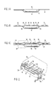
- FIG. 1A an intermediate stage of manufacture of this device is first portrayed.
- An integrated circuit device is placed in a recessed chip mount pad 12 of a first lead frame 14.
- a lead frame is well known in the art as represented by the prior art discussed herein.
- the integrated circuit chip is back bonded in the zone 16 to anchor the device onto the frame.
- the term "chip” is generic to known semiconductor devices. Back bonding uses a suitable adhesive such as epoxies and polyimides.
- a double sided adhesive tape 24 is placed on both the lead frame 14 and the top of the semiconductor device 10.
- the tape is typically, high temperature polyimide film such as duPont KaptonTM having two sided adhesive which is typically a phenolic or polyimide, silicone or acrylic material or combination thereof.
- the tape 24 is a three layer composite of polyimide film coated with adhesive.
- the tape is applied as parallel strips across the periphery of the lead frame and to the semiconductor device in zones between the peripheral pads 22 and a central pads 26. That is, the tape 24 is applied to both the top surface of the chip, to the inner lead frame conductors and over the dam bar.
- the tape also serves as an insulator and an alpha barrier. Such are well known as in U.S. Patent 4,426,647. The barrier may be between 1.6 and 2 mils thick.
- a series of wire bonds 18 extend from a lead frame finger 20 to a peripheral pad 22 located on a major surface device 10. It will be understood that while Figure 1B illustrates two such connections, there may be a plurality of such peripheral pads 22 around the device 10 with elective bonding as the circuitry so requires. Alternatively, the wire bonds 18 may be made before the tape 24 is placed down.
- FIG 1C shows the next intermediate step in the manufacture of the module in accordance with this invention.
- a second lead frame 28 is placed over the tape 24.
- tape 24 may be placed on lead frame 28 prior to placement of the lead frame 28, over the assembly illustrated in Figure 1B, (in such a step, the tape would not be present on frame 14 or device 10).
- the second lead frame 28 has its fingers 30 resting on the tape areas 24 on the semiconductor device 10. Then, the lead frame fingers 30 have selected wire bonds made to the central terminals 26 via wires 32.
- the module processing then proceeds to the formation of a molded plastic body 34 which encapsulates both lead frames and the semiconductor chip.
- the molding is typically by known transfer molding techniques. Following encapsulation lead frame selvage is removed.
- both the two lead frames provide contacts to pads 36, 38 on an integrated circuit board to which completed subassembly are mounted.
- the peripherally extending terminal leads of both lead frames 14 and 28 protrude through the sides of the package 34 and are turned downward to form "J lead" contact surfaces 39. It will be appreciated that while only two such leads are illustrated on each side, in fact there will be many such leads in the intricacy of such lead frames.
- the completed package provides two lead frames which provide both wire bonds on the peripheral input/output pads but also in the center area input/output pads of the semiconductor device.
- the package allows for wire bonding and plastic molding of chips which contain both peripheral and area input/output pads.
- the package allows for reduced line loss due to the shorter area wire lengths which may be used. This in turn increases the package I/O capability.
- This invention by separating the leads both horizontally as well as vertically and to different rows of pads, allows for electrical decoupling of leads.
- power distribution and signal paths may be decoupled by proper assignment of leads to minimize crosstalk.
- the insulative tape provides increased thermal performance by providing a discreet zone of separation between the two lead frames and more particularly, the upper lead frame 28 laminated to chip major surface. Such is important as packing density increases.
- the invention also provides for flexibility heretofore not known in this technology. By the use of at least two vertically displaced frames customized lead output location may occur. Moreover, as illustrated in Figure 2, engineering change capability is provided through alterable I/O avoiding chip redesign at the card or the circuit board level.
- This invention while shown applicable to a generic integrated circuit device, is also applicable to quad lead packages, small outline packaging and hybrid packaging techniques. That is, it can be used with both ceramic as well as plastic packaging. Importantly, the package provides complete alpha protection to the chip.
Landscapes
- Physics & Mathematics (AREA)
- Condensed Matter Physics & Semiconductors (AREA)
- General Physics & Mathematics (AREA)
- Engineering & Computer Science (AREA)
- Computer Hardware Design (AREA)
- Microelectronics & Electronic Packaging (AREA)
- Power Engineering (AREA)
- Lead Frames For Integrated Circuits (AREA)
- Credit Cards Or The Like (AREA)
Applications Claiming Priority (2)
| Application Number | Priority Date | Filing Date | Title |
|---|---|---|---|
| US61361 | 1987-06-15 | ||
| US07/061,361 US4796078A (en) | 1987-06-15 | 1987-06-15 | Peripheral/area wire bonding technique |
Publications (2)
| Publication Number | Publication Date |
|---|---|
| EP0295459A2 true EP0295459A2 (fr) | 1988-12-21 |
| EP0295459A3 EP0295459A3 (fr) | 1989-10-18 |
Family
ID=22035304
Family Applications (1)
| Application Number | Title | Priority Date | Filing Date |
|---|---|---|---|
| EP88108218A Withdrawn EP0295459A3 (fr) | 1987-06-15 | 1988-05-24 | Assemblage électronique et son procédé de fabrication |
Country Status (3)
| Country | Link |
|---|---|
| US (1) | US4796078A (fr) |
| EP (1) | EP0295459A3 (fr) |
| JP (1) | JPH0831560B2 (fr) |
Cited By (4)
| Publication number | Priority date | Publication date | Assignee | Title |
|---|---|---|---|---|
| EP0447922A1 (fr) * | 1990-03-13 | 1991-09-25 | Kabushiki Kaisha Toshiba | Dispositif semi-conducteur du type à encapsulation par résine |
| EP0533589A1 (fr) * | 1991-09-20 | 1993-03-24 | Fujitsu Limited | Dispositif semi-conducteur |
| GB2305000A (en) * | 1995-08-23 | 1997-03-26 | Schlumberger Ind Sa | Micropackage for an electronic memory card |
| EP0987758A2 (fr) * | 1991-12-27 | 2000-03-22 | Fujitsu Limited | Dispositif semi-conducteur et procédé pour fabriquer celui-ci |
Families Citing this family (80)
| Publication number | Priority date | Publication date | Assignee | Title |
|---|---|---|---|---|
| US5917707A (en) | 1993-11-16 | 1999-06-29 | Formfactor, Inc. | Flexible contact structure with an electrically conductive shell |
| US5365113A (en) * | 1987-06-30 | 1994-11-15 | Hitachi, Ltd. | Semiconductor device |
| US5184208A (en) * | 1987-06-30 | 1993-02-02 | Hitachi, Ltd. | Semiconductor device |
| JP2708191B2 (ja) * | 1988-09-20 | 1998-02-04 | 株式会社日立製作所 | 半導体装置 |
| JP2522524B2 (ja) * | 1988-08-06 | 1996-08-07 | 株式会社東芝 | 半導体装置の製造方法 |
| KR0158868B1 (ko) * | 1988-09-20 | 1998-12-01 | 미다 가쓰시게 | 반도체장치 |
| US5311056A (en) * | 1988-10-21 | 1994-05-10 | Shinko Electric Industries Co., Ltd. | Semiconductor device having a bi-level leadframe |
| US5099306A (en) * | 1988-11-21 | 1992-03-24 | Honeywell Inc. | Stacked tab leadframe assembly |
| US5089878A (en) * | 1989-06-09 | 1992-02-18 | Lee Jaesup N | Low impedance packaging |
| US4987473A (en) * | 1989-08-03 | 1991-01-22 | Vlsi Technology, Inc. | Leadframe system with multi-tier leads |
| US5291060A (en) * | 1989-10-16 | 1994-03-01 | Shinko Electric Industries Co., Ltd. | Lead frame and semiconductor device using same |
| US5237202A (en) * | 1989-10-16 | 1993-08-17 | Shinko Electric Industries Co., Ltd | Lead frame and semiconductor device using same |
| US4965654A (en) * | 1989-10-30 | 1990-10-23 | International Business Machines Corporation | Semiconductor package with ground plane |
| US5256903A (en) * | 1990-02-28 | 1993-10-26 | Hitachi Ltd. | Plastic encapsulated semiconductor device |
| US5147815A (en) * | 1990-05-14 | 1992-09-15 | Motorola, Inc. | Method for fabricating a multichip semiconductor device having two interdigitated leadframes |
| US5227662A (en) * | 1990-05-24 | 1993-07-13 | Nippon Steel Corporation | Composite lead frame and semiconductor device using the same |
| US5377077A (en) * | 1990-08-01 | 1994-12-27 | Staktek Corporation | Ultra high density integrated circuit packages method and apparatus |
| EP0509065A1 (fr) * | 1990-08-01 | 1992-10-21 | Staktek Corporation | Procede et appareil de production de boitiers de circuits integres de densite ultra-elevee |
| US5475920A (en) * | 1990-08-01 | 1995-12-19 | Burns; Carmen D. | Method of assembling ultra high density integrated circuit packages |
| US5367766A (en) * | 1990-08-01 | 1994-11-29 | Staktek Corporation | Ultra high density integrated circuit packages method |
| US5446620A (en) * | 1990-08-01 | 1995-08-29 | Staktek Corporation | Ultra high density integrated circuit packages |
| US5148266A (en) * | 1990-09-24 | 1992-09-15 | Ist Associates, Inc. | Semiconductor chip assemblies having interposer and flexible lead |
| US5148265A (en) | 1990-09-24 | 1992-09-15 | Ist Associates, Inc. | Semiconductor chip assemblies with fan-in leads |
| US7198969B1 (en) * | 1990-09-24 | 2007-04-03 | Tessera, Inc. | Semiconductor chip assemblies, methods of making same and components for same |
| US20010030370A1 (en) * | 1990-09-24 | 2001-10-18 | Khandros Igor Y. | Microelectronic assembly having encapsulated wire bonding leads |
| US5258330A (en) * | 1990-09-24 | 1993-11-02 | Tessera, Inc. | Semiconductor chip assemblies with fan-in leads |
| US5679977A (en) * | 1990-09-24 | 1997-10-21 | Tessera, Inc. | Semiconductor chip assemblies, methods of making same and components for same |
| KR920007161A (ko) * | 1990-09-26 | 1992-04-28 | 기따지마 요시도기 | 다층 리드프레임(lead frame), 이 다층 리드프레임에 사용되는 도전판 및 이 도전판의 제조방법 |
| US5124503A (en) * | 1990-12-13 | 1992-06-23 | Allied-Signal Inc. | Dichlorotrifluoroethane stabilized to minimize hydrolysis thereof |
| JP2501246B2 (ja) * | 1991-01-21 | 1996-05-29 | 株式会社東芝 | 半導体装置 |
| AU1665392A (en) * | 1991-04-05 | 1992-11-02 | Allied-Signal Inc. | Stabilized dichlorotrifluoroethane refrigeration compositions |
| KR940006164B1 (ko) * | 1991-05-11 | 1994-07-08 | 금성일렉트론 주식회사 | 반도체 패키지 및 그 제조방법 |
| US5448450A (en) * | 1991-08-15 | 1995-09-05 | Staktek Corporation | Lead-on-chip integrated circuit apparatus |
| US5451813A (en) * | 1991-09-05 | 1995-09-19 | Rohm Co., Ltd. | Semiconductor device with lead frame having different thicknesses |
| JP2609382B2 (ja) * | 1991-10-01 | 1997-05-14 | 三菱電機株式会社 | 半導体装置 |
| JP2634516B2 (ja) * | 1991-10-15 | 1997-07-30 | 三菱電機株式会社 | 反転型icの製造方法、反転型ic、icモジュール |
| JPH0538951U (ja) * | 1991-10-28 | 1993-05-25 | ブラザー工業株式会社 | 表面実装部品の回路基板への実装構造 |
| JPH05206354A (ja) * | 1992-01-24 | 1993-08-13 | Mitsubishi Electric Corp | 半導体圧力センサおよびその製造方法 |
| KR100276781B1 (ko) * | 1992-02-03 | 2001-01-15 | 비센트 비. 인그라시아 | 리드-온-칩 반도체장치 및 그 제조방법 |
| US5702985A (en) * | 1992-06-26 | 1997-12-30 | Staktek Corporation | Hermetically sealed ceramic integrated circuit heat dissipating package fabrication method |
| US5380952A (en) * | 1992-07-22 | 1995-01-10 | Vlsi Technology, Inc. | Integrated circuit package with stabilizer bar |
| JPH077121A (ja) * | 1992-09-18 | 1995-01-10 | Texas Instr Inc <Ti> | 多層リードフレームアセンブリを有する半導体デバイスおよびそのパッケージ方法 |
| US5484959A (en) * | 1992-12-11 | 1996-01-16 | Staktek Corporation | High density lead-on-package fabrication method and apparatus |
| US6205654B1 (en) | 1992-12-11 | 2001-03-27 | Staktek Group L.P. | Method of manufacturing a surface mount package |
| US5399902A (en) * | 1993-03-04 | 1995-03-21 | International Business Machines Corporation | Semiconductor chip packaging structure including a ground plane |
| US5369056A (en) * | 1993-03-29 | 1994-11-29 | Staktek Corporation | Warp-resistent ultra-thin integrated circuit package fabrication method |
| US5644161A (en) * | 1993-03-29 | 1997-07-01 | Staktek Corporation | Ultra-high density warp-resistant memory module |
| US5541812A (en) * | 1995-05-22 | 1996-07-30 | Burns; Carmen D. | Bus communication system for stacked high density integrated circuit packages having an intermediate lead frame |
| US5455740A (en) * | 1994-03-07 | 1995-10-03 | Staktek Corporation | Bus communication system for stacked high density integrated circuit packages |
| US5801437A (en) * | 1993-03-29 | 1998-09-01 | Staktek Corporation | Three-dimensional warp-resistant integrated circuit module method and apparatus |
| US5820014A (en) | 1993-11-16 | 1998-10-13 | Form Factor, Inc. | Solder preforms |
| US7073254B2 (en) * | 1993-11-16 | 2006-07-11 | Formfactor, Inc. | Method for mounting a plurality of spring contact elements |
| AU2231795A (en) * | 1994-04-14 | 1995-11-10 | Olin Corporation | Electronic package having improved wire bonding capability |
| JPH07288309A (ja) * | 1994-04-19 | 1995-10-31 | Mitsubishi Electric Corp | 半導体装置及びその製造方法並びに半導体モジュール |
| US5661336A (en) * | 1994-05-03 | 1997-08-26 | Phelps, Jr.; Douglas Wallace | Tape application platform and processes therefor |
| US5923538A (en) * | 1994-10-17 | 1999-07-13 | Lsi Logic Corporation | Support member for mounting a microelectronic circuit package |
| US6025642A (en) * | 1995-08-17 | 2000-02-15 | Staktek Corporation | Ultra high density integrated circuit packages |
| US6551845B1 (en) * | 1996-01-02 | 2003-04-22 | Micron Technology, Inc. | Method of temporarily securing a die to a burn-in carrier |
| US8033838B2 (en) * | 1996-02-21 | 2011-10-11 | Formfactor, Inc. | Microelectronic contact structure |
| US5994152A (en) | 1996-02-21 | 1999-11-30 | Formfactor, Inc. | Fabricating interconnects and tips using sacrificial substrates |
| US5776799A (en) * | 1996-11-08 | 1998-07-07 | Samsung Electronics Co., Ltd. | Lead-on-chip type semiconductor chip package using an adhesive deposited on chip active surfaces at a wafer level and method for manufacturing same |
| JP3535328B2 (ja) * | 1996-11-13 | 2004-06-07 | 株式会社ルネサステクノロジ | リードフレームとこれを用いた半導体装置 |
| US5937276A (en) * | 1996-12-13 | 1999-08-10 | Tessera, Inc. | Bonding lead structure with enhanced encapsulation |
| US6068180A (en) * | 1996-12-18 | 2000-05-30 | Texas Instruments Incorporated | System, apparatus, and method for connecting a semiconductor chip to a three-dimensional leadframe |
| US6462404B1 (en) * | 1997-02-28 | 2002-10-08 | Micron Technology, Inc. | Multilevel leadframe for a packaged integrated circuit |
| US5945732A (en) * | 1997-03-12 | 1999-08-31 | Staktek Corporation | Apparatus and method of manufacturing a warp resistant thermally conductive integrated circuit package |
| US6687969B1 (en) | 1997-05-16 | 2004-02-10 | Micron Technology, Inc. | Methods of fixturing flexible substrates and methods of processing flexible substrates |
| US5972152A (en) | 1997-05-16 | 1999-10-26 | Micron Communications, Inc. | Methods of fixturing flexible circuit substrates and a processing carrier, processing a flexible circuit and processing a flexible circuit substrate relative to a processing carrier |
| US6774480B1 (en) | 1999-07-30 | 2004-08-10 | Micron Technology, Inc. | Method and structure for manufacturing improved yield semiconductor packaged devices |
| US6572387B2 (en) | 1999-09-24 | 2003-06-03 | Staktek Group, L.P. | Flexible circuit connector for stacked chip module |
| US6762067B1 (en) * | 2000-01-18 | 2004-07-13 | Fairchild Semiconductor Corporation | Method of packaging a plurality of devices utilizing a plurality of lead frames coupled together by rails |
| US6608763B1 (en) | 2000-09-15 | 2003-08-19 | Staktek Group L.P. | Stacking system and method |
| US6462408B1 (en) | 2001-03-27 | 2002-10-08 | Staktek Group, L.P. | Contact member stacking system and method |
| JP2003234359A (ja) * | 2002-02-08 | 2003-08-22 | Hitachi Ltd | 半導体装置の製造方法 |
| US20040105244A1 (en) * | 2002-08-06 | 2004-06-03 | Ilyas Mohammed | Lead assemblies with offset portions and microelectronic assemblies with leads having offset portions |
| US8120153B1 (en) | 2005-09-16 | 2012-02-21 | University Of Central Florida Research Foundation, Inc. | High-temperature, wirebondless, injection-molded, ultra-compact hybrid power module |
| US7808088B2 (en) * | 2006-06-07 | 2010-10-05 | Texas Instruments Incorporated | Semiconductor device with improved high current performance |
| US8435837B2 (en) * | 2009-12-15 | 2013-05-07 | Silicon Storage Technology, Inc. | Panel based lead frame packaging method and device |
| DE102010044709B4 (de) * | 2010-09-08 | 2015-07-02 | Vincotech Holdings S.à.r.l. | Leistungshalbleitermodul mit Metallsinterverbindungen sowie Herstellungsverfahren |
| DE102020109493A1 (de) | 2020-04-06 | 2021-10-07 | Infineon Technologies Ag | Ein halbleiterbauelementpackage mit zwei übereinander gestapelten leadframes |
Citations (2)
| Publication number | Priority date | Publication date | Assignee | Title |
|---|---|---|---|---|
| US4496965A (en) * | 1981-05-18 | 1985-01-29 | Texas Instruments Incorporated | Stacked interdigitated lead frame assembly |
| EP0228869A2 (fr) * | 1986-01-06 | 1987-07-15 | AT&T Corp. | Méthode de fabrication d'un paquetage pour un composant électronique |
Family Cites Families (12)
| Publication number | Priority date | Publication date | Assignee | Title |
|---|---|---|---|---|
| US3838984A (en) * | 1973-04-16 | 1974-10-01 | Sperry Rand Corp | Flexible carrier and interconnect for uncased ic chips |
| JPS5229060U (fr) * | 1975-08-20 | 1977-03-01 | ||
| JPS5372456A (en) * | 1976-12-10 | 1978-06-27 | Hitachi Ltd | Glass sealing semiconductor device |
| US4330790A (en) * | 1980-03-24 | 1982-05-18 | National Semiconductor Corporation | Tape operated semiconductor device packaging |
| ZA812893B (en) * | 1980-05-12 | 1982-05-26 | Ncr Co | Integrated circuit package having a plurality of pins for providing external electrical connections |
| US4438181A (en) * | 1981-01-13 | 1984-03-20 | Jon M. Schroeder | Electronic component bonding tape |
| JPS59127843A (ja) * | 1983-01-12 | 1984-07-23 | Fujitsu Ltd | 半導体装置の製造方法 |
| JPS6020525A (ja) * | 1983-07-13 | 1985-02-01 | Matsushita Electronics Corp | 半導体装置 |
| JPS6112053A (ja) * | 1984-06-27 | 1986-01-20 | Nec Corp | リ−ドフレ−ム |
| CA1238119A (fr) * | 1985-04-18 | 1988-06-14 | Douglas W. Phelps, Jr. | Microplaquette conditionee |
| JPH0812896B2 (ja) * | 1985-04-19 | 1996-02-07 | 松下電子工業株式会社 | 半導体装置 |
| JPS6240752A (ja) * | 1985-08-16 | 1987-02-21 | Fujitsu Ltd | 半導体装置 |
-
1987
- 1987-06-15 US US07/061,361 patent/US4796078A/en not_active Expired - Lifetime
-
1988
- 1988-04-20 JP JP63095826A patent/JPH0831560B2/ja not_active Expired - Lifetime
- 1988-05-24 EP EP88108218A patent/EP0295459A3/fr not_active Withdrawn
Patent Citations (2)
| Publication number | Priority date | Publication date | Assignee | Title |
|---|---|---|---|---|
| US4496965A (en) * | 1981-05-18 | 1985-01-29 | Texas Instruments Incorporated | Stacked interdigitated lead frame assembly |
| EP0228869A2 (fr) * | 1986-01-06 | 1987-07-15 | AT&T Corp. | Méthode de fabrication d'un paquetage pour un composant électronique |
Non-Patent Citations (1)
| Title |
|---|
| PATENT ABSTRACTS OF JAPAN, vol. 10, no. 158 (E-409)[2214], 6th June 1986; & JP-A-61 012 053 (NIPPON DENKI K.K.) 20-01-1986 * |
Cited By (7)
| Publication number | Priority date | Publication date | Assignee | Title |
|---|---|---|---|---|
| EP0447922A1 (fr) * | 1990-03-13 | 1991-09-25 | Kabushiki Kaisha Toshiba | Dispositif semi-conducteur du type à encapsulation par résine |
| EP0533589A1 (fr) * | 1991-09-20 | 1993-03-24 | Fujitsu Limited | Dispositif semi-conducteur |
| US5648680A (en) * | 1991-09-20 | 1997-07-15 | Fujitsu Limited | Lead-on-chip semiconductor device |
| EP0987758A2 (fr) * | 1991-12-27 | 2000-03-22 | Fujitsu Limited | Dispositif semi-conducteur et procédé pour fabriquer celui-ci |
| EP0987758A3 (fr) * | 1991-12-27 | 2000-05-24 | Fujitsu Limited | Dispositif semi-conducteur et procédé pour fabriquer celui-ci |
| GB2305000A (en) * | 1995-08-23 | 1997-03-26 | Schlumberger Ind Sa | Micropackage for an electronic memory card |
| GB2305000B (en) * | 1995-08-23 | 1997-08-06 | Schlumberger Ind Sa | Electronic micropackage for an electric memory card, and a method of making such a package |
Also Published As
| Publication number | Publication date |
|---|---|
| JPS6428945A (en) | 1989-01-31 |
| JPH0831560B2 (ja) | 1996-03-27 |
| EP0295459A3 (fr) | 1989-10-18 |
| US4796078A (en) | 1989-01-03 |
Similar Documents
| Publication | Publication Date | Title |
|---|---|---|
| US4796078A (en) | Peripheral/area wire bonding technique | |
| US6261865B1 (en) | Multi chip semiconductor package and method of construction | |
| CA1217876A (fr) | Dispositif semiconducteur, et sa fabrication | |
| EP0247775B1 (fr) | Empaquetage pour semi-conducteurs ayant des connexions entrée/sortie à haute densité | |
| EP0498446B1 (fr) | Dispositif encapsulé à plusieurs puces semi-conductrices et procédé pour sa fabrication | |
| US6482674B1 (en) | Semiconductor package having metal foil die mounting plate | |
| US5637828A (en) | High density semiconductor package | |
| US7008824B2 (en) | Method of fabricating mounted multiple semiconductor dies in a package | |
| US5620928A (en) | Ultra thin ball grid array using a flex tape or printed wiring board substrate and method | |
| EP0962975B1 (fr) | Empaquetage de MOSFET de puissance avec des broches à connexion directe | |
| EP0424530B1 (fr) | Dispositif semi-conducteur scelle a la resine | |
| US6977190B2 (en) | Semiconductor device and method for production thereof | |
| EP0488783A2 (fr) | Cadre conducteur pour dispositif semi-conducteur comprenant un dissipateur de chaleur | |
| EP0340241A4 (fr) | Boitier electronique a haute densite comprenant des sous-modules empiles. | |
| KR920001689A (ko) | 반도체장치 및 그 제조방법 | |
| JP2953899B2 (ja) | 半導体装置 | |
| JPH09252065A (ja) | 半導体装置及びその製造方法及び基板フレーム | |
| US5296737A (en) | Semiconductor device with a plurality of face to face chips | |
| USRE36894E (en) | Semiconductor package with high density I/O lead connection | |
| EP0474224B1 (fr) | Dispositif semi-conducteur comprenant une pluralité de puces semi-conductrices | |
| JPS6370532A (ja) | 半導体装置 | |
| KR100221918B1 (ko) | 칩 스케일 패키지 | |
| JPH06216492A (ja) | 電子装置 | |
| JPH0810746B2 (ja) | メモリーモジュール | |
| KR100216065B1 (ko) | 멀티 리드 온 칩 패키지 |
Legal Events
| Date | Code | Title | Description |
|---|---|---|---|
| PUAI | Public reference made under article 153(3) epc to a published international application that has entered the european phase |
Free format text: ORIGINAL CODE: 0009012 |
|
| AK | Designated contracting states |
Kind code of ref document: A2 Designated state(s): DE FR GB |
|
| 17P | Request for examination filed |
Effective date: 19890413 |
|
| PUAL | Search report despatched |
Free format text: ORIGINAL CODE: 0009013 |
|
| AK | Designated contracting states |
Kind code of ref document: A3 Designated state(s): DE FR GB |
|
| 17Q | First examination report despatched |
Effective date: 19910612 |
|
| STAA | Information on the status of an ep patent application or granted ep patent |
Free format text: STATUS: THE APPLICATION IS DEEMED TO BE WITHDRAWN |
|
| 18D | Application deemed to be withdrawn |
Effective date: 19920102 |