EP0280883B1 - Equipement de mémoire permanente à semi-conducteur - Google Patents
Equipement de mémoire permanente à semi-conducteur Download PDFInfo
- Publication number
- EP0280883B1 EP0280883B1 EP88101335A EP88101335A EP0280883B1 EP 0280883 B1 EP0280883 B1 EP 0280883B1 EP 88101335 A EP88101335 A EP 88101335A EP 88101335 A EP88101335 A EP 88101335A EP 0280883 B1 EP0280883 B1 EP 0280883B1
- Authority
- EP
- European Patent Office
- Prior art keywords
- line
- voltage
- gate electrode
- data
- read
- Prior art date
- Legal status (The legal status is an assumption and is not a legal conclusion. Google has not performed a legal analysis and makes no representation as to the accuracy of the status listed.)
- Expired - Lifetime
Links
- 239000004065 semiconductor Substances 0.000 title claims description 19
- 238000009792 diffusion process Methods 0.000 claims description 47
- 239000000758 substrate Substances 0.000 claims description 7
- 238000010586 diagram Methods 0.000 description 14
- 230000003247 decreasing effect Effects 0.000 description 9
- 230000005684 electric field Effects 0.000 description 8
- 229910021420 polycrystalline silicon Inorganic materials 0.000 description 7
- 229920005591 polysilicon Polymers 0.000 description 7
- 238000002347 injection Methods 0.000 description 4
- 239000007924 injection Substances 0.000 description 4
- 230000014759 maintenance of location Effects 0.000 description 4
- 230000002093 peripheral effect Effects 0.000 description 4
- 238000007796 conventional method Methods 0.000 description 2
- 230000000694 effects Effects 0.000 description 2
- 238000009413 insulation Methods 0.000 description 2
- 230000007423 decrease Effects 0.000 description 1
- 230000000593 degrading effect Effects 0.000 description 1
- 238000007599 discharging Methods 0.000 description 1
- 230000006870 function Effects 0.000 description 1
- 238000004519 manufacturing process Methods 0.000 description 1
Images


Classifications
-
- G—PHYSICS
- G11—INFORMATION STORAGE
- G11C—STATIC STORES
- G11C17/00—Read-only memories programmable only once; Semi-permanent stores, e.g. manually-replaceable information cards
-
- G—PHYSICS
- G11—INFORMATION STORAGE
- G11C—STATIC STORES
- G11C16/00—Erasable programmable read-only memories
- G11C16/02—Erasable programmable read-only memories electrically programmable
- G11C16/06—Auxiliary circuits, e.g. for writing into memory
- G11C16/26—Sensing or reading circuits; Data output circuits
-
- G—PHYSICS
- G11—INFORMATION STORAGE
- G11C—STATIC STORES
- G11C16/00—Erasable programmable read-only memories
- G11C16/02—Erasable programmable read-only memories electrically programmable
- G11C16/04—Erasable programmable read-only memories electrically programmable using variable threshold transistors, e.g. FAMOS
- G11C16/0408—Erasable programmable read-only memories electrically programmable using variable threshold transistors, e.g. FAMOS comprising cells containing floating gate transistors
- G11C16/0433—Erasable programmable read-only memories electrically programmable using variable threshold transistors, e.g. FAMOS comprising cells containing floating gate transistors comprising cells containing a single floating gate transistor and one or more separate select transistors
-
- G—PHYSICS
- G11—INFORMATION STORAGE
- G11C—STATIC STORES
- G11C16/00—Erasable programmable read-only memories
- G11C16/02—Erasable programmable read-only memories electrically programmable
- G11C16/06—Auxiliary circuits, e.g. for writing into memory
- G11C16/10—Programming or data input circuits
Definitions
- the present invention relates to a nonvolatile semiconductor memory in which data can be electrically rewritten using nonvolatile transistors.
- E2PROM Electrically Erasable and Programmable Read Only Memory
- E2PROMs can have any of a number of different memory cell structures, most, however, tend to be of floating gate type structure, in which a floating gate electrode partially overlaps a diffusion layer, through a thin insulating film.
- Fig. 1 is a sectional view showing the structure of one such conventional memory cell.
- N-type diffusion layers 11, 12, and 13 are formed in a surface of p-type semiconductor substrate 10.
- Channel region 14 is formed between diffusion layers 11 and 12.
- Polysilicon electrode 16 is formed above channel region 14 and parts of diffusion layers 11 and 12.
- One portion of electrode 16 is thicker than the remainder thereof and is formed above diffusion layer 12.
- Insulation film 15 (described in detail later) is formed between substrate 10 and polysilicon electrode 16.
- This film 15 has thin insulation film 17 located between diffusion layer 12 and the thicker portion of electrode 16.
- polysilicon electrode 19 is formed above electrode 16 interposing insulating film 18 having a thickness almost equal to that of insulating film 15.
- Channel region 20 is formed between diffusion layers 12 and 13.
- Polysilicon electrode 22 is formed above channel region 20 interposing insulating film 21 having a thickness almost equal to that of insulating film 15.
- Diffusion layers 11 and 13 are respectively connected to source wiring S and bit line BL. Electrodes 16, 19, and 22 are respectively used as a floating gate electrode, a control gate electrode, and a gate electrode. Control gate electrode 19 and gate electrode 22 are connected to control gate line CG and selection gate line SG, respectively.
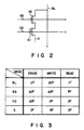
- Fig. 2 is an equivalent circuit diagram of the conventional cell having the structure shown in Fig. 1.
- Transistor 41 as shown in Fig. 2, is of floating gate type. Diffusion layers 11 and 12 of transistor 41 are used as a source and a drain, respectively, transistor 41 itself constituting a memory transistor for storing data.
- Transistor 42 is of normal MOS type. Diffusion layers 12 and 13 of transistor 42 are used as a source and a drain, respectively, transistor 42 itself constituting a selection transistor for selecting memory transistor 41.
- Fig. 3 is a table which shows the voltages applied to source wiring S, bit line BL, control gate line CG, and selection gate line SG in each mode.
- ground power source GND 0 V
- read power source voltage Vcc 5 V
- write power source voltage Vpp 20 V.
- write power source voltage Vpp is not supplied by an external power source, but is generated in the integrated circuit itself by boosting read power source voltage Vcc.
- the data erase mode which is also known as the electron injecting mode, will now be described.
- threshold voltage V TH In the data erase mode, electrons are injected into floating gate electrode 16, to increase threshold voltage V TH of memory transistor 41.
- bit line BL 0 V
- selection gate line SG 20 V
- control gate line CG 20 V
- source wiring S 0 V.
- selection gate line SG 20 V
- selection transistor 42 By setting selection gate line SG at 20 V, selection transistor 42 is rendered conductive, and the potential at n-type diffusion layer 12 becomes equal to that at bit line BL, i.e., 0 V.
- a high voltage is applied to floating gate electrode 16 from control gate line CG, and a high electric field is applied to thin insulating film 17 between floating gate electrode 16 and n-type diffusion layer 12.
- threshold voltage V TH is increased up to, e.g., about 8 V.
- the data write mode also known as the electron discharge mode, will now be described.
- threshold voltage V TH of memory transistor 41 is decreased by discharging the electrons which were injected into floating gate electrode 16.
- bit line BL 20 V
- selection gate line SG 20 V
- control gate line CG 0 V
- source wiring S 5 V. That is, the floating gate electrode 16 is set in a floating state.
- selection transistor 42 is rendered conductive and the potential at n-type diffusion layer 12 becomes equal to that at bit line BL, i.e., 20 V.
- a high electric field is applied to thin insulating film 17, in the opposite direction to that in the erase mode, the electrons are discharged from floating gate electrode 16 into n-type diffusion layer 12 by tunnel current. As a result, thereby decreasing threshold voltage V TH of memory transistor 41 to, for example, -5 V.
- bit line BL 1 V
- selection gate line SG 5 V
- control gate line CG 0 V
- source wiring S 0 V.
- selection gate line SG 5 V
- selection transistor 42 is rendered conductive, and the potential at n-type diffusion layer 12 becomes equal to that at bit line BL, i.e., 1 V.
- memory transistor 41 is not rendered conductive, this being due to threshold voltage V TH having been increased. For this reason, no current flows between bit line BL and source wiring S, and hence the potential at bit line BL is kept at 1 V.
- bit line BL when the electrons are discharged from floating gate electrode 16, memory transistor 41 is rendered conductive, due to threshold voltage V TH being decreased. In these circumstances, current flows between bit line BL and source wiring S, and the potential at bit line BL becomes equal to that at source wiring S, i.e., 0 V. More specifically, logic "1" or "0" level is determined by amplifying the potential difference between 1 V and 0 V at bit line BL, using a sense amplifier (not shown) connected to bit line BL.
- bit line BL The reason the potential at bit line BL must be limited to as low as 1 V and not increased up to 5 V in the read mode will now be explained below.
- bit line BL is set at 5 V in the read mode, the potential at n-type diffusion layer 12 becomes almost 5 V.
- an electric field generated by the potential difference between 0 V of control gate line CG and 5 V of n-type diffusion layer 12 is applied to thin insulating film 17 through floating gate electrode 16.
- this electric field is applied in the same direction as that in the write mode (electron discharge mode).
- the only difference, in this case, is that the intensity of this electric field is lower than that in the write mode. consequently, if a cell in which electrons are injected, is set in the read mode for a long period of time, the injected electrons are gradually discharged from floating gate electrode 16 because of the tunnel effect.
- threshold voltage V TH gradually decreases, which may give rise to a logical operation error occurring after a certain period of time.
- Such a phenomenon is known as a soft write (insufficient write) phenomenon.
- the retentivity of data as a function of time, in the event of a soft write phenomenon occurring is known as the read retention characteristic (data retentivity in the read mode).
- bit line BL is set at about 1 V to sufficiently improve the read retention characteristic.
- a small logical margin is compensated using a high-performance sense amplifier or the like, and hence the sense amplifier is overloaded.
- the sense amplifier since the sense amplifier is overloaded, various problems are posed as follows.
- the arrangement of the sense amplifier is complicated, and the chip area of semiconductor memory is increased when the sense amplifier is formed into an integrated circuit.
- the increase in the chip area leads to an increase in manufacturing cost.
- the margin of operational power source voltage in the read mode is reduced, and especially, operation performance in a low-voltage range is degraded.
- a constant voltage source is required to apply an intermediate voltage of 1 V to bit line BL. If a circuit for generating such an intermediate voltage is incorporated in the sense amplifier, a current consumption is increased and this is disadvantageous in terms of power consumption.
- the access time is increased.
- the present invention provides a nonvolatile semiconductor memory as stated in claim 1.
- Fig. 4 is a sectional view showing the arrangement of a memory cell used in the nonvolatile semiconductor memory according to the present invention.
- N-type diffusion layers 11, 12, and 13 are formed in the surface of p-type semiconductor substrate 10.
- Channel region 14 is formed between diffusion layers 11 and 12.
- Polysilicon electrode 16 is formed above channel region 14, through relatively thick insulating film 15.
- electrode 16 overlaps n-type diffusion layer 12, through insulating film 17 which is thinner than insulating film 15.
- Polysilicon electrode 19 is formed above electrode 16, through relatively thick insulating film 18.
- Channel region 20 is formed between diffusion layers 12 and 13.
- Polysilicon electrode 22 is formed above channel region 20, through relatively thick insulating film 21.
- Read and write lines RL and WL are connected to diffusion layers 11 and 13, respectively. Electrodes 16, 19, and 22 are respectively used as a floating gate electrode, a control gate electrode, and a gate electrode. Electrodes 19 and 22 are connected to control gate line CG and selection gate line SG, respectively.
- Fig. 5 shows an equivalent circuit diagram of the cell shown in Fig. 4.
- Transistor 31, as shown in Fig. 5, is of floating gate type. Diffusion layers 11 and 12 of transistor 31 are used as a source and a drain, respectively, transistor 31 itself constituting a memory transistor for storing data.
- Transistor 32 is of normal MOS type. Diffusion layers 12 and 13 of transistor 32 are used as a source and a drain, respectively, transistor 32 itself constituting a selection transistor for selecting memory transistor 31.
- Fig. 6 is a table which shows the voltages applied to read line RL, write line WL, control gate line CG, and selection gate line SG in each mode.
- write line WL 0 V
- selection gate line SG 20 V
- control gate line CG 20 V
- read line RL 0 V.
- selection transistor 32 is rendered conductive, and the potential at n-type diffusion layer 12 becomes equal to that of write line WL, i.e., 0 V.
- a high voltage is applied to floating gate electrode 16, through control gate line CG. Therefore, a high electric field is applied to thin insulating film 17 between floating gate electrode 16 and n-type diffusion layer 12, and electrons are injected into the floating gate electrode 16 from n-type diffusion layer 12 by tunnel current.
- threshold voltage V TH of memory transistor 31 is increased to, for example, 8 V.
- write line WL 20 V
- selection gate line SG 20 V
- control gate line CG 0 V
- read line RL 5 V.
- selection transistor 32 is rendered conductive, and the potential of n-type diffusion layer 12 becomes equal to write line WL, i.e., 20 V.
- a high electric field is applied to thin insulating film 17, in the opposite direction to that in the erase mode. Consequently, the electrons are discharged from floating gate electrode 16 into n-type diffusion layer 12 by tunnel current.
- threshold voltage V TH of memory transistor 31 is decreased to, for example, -5 V. Accordingly, in the data erase and write modes, the same operation is performed as in the conventional cell.
- write line WL 0 V
- selection gate line SG 5 V
- control gate line CG 0 V
- read line RL 5 V.
- selection transistor 32 is rendered conductive, the potential at n-type diffusion layer 12 becomes equal to that at write line WL, i.e., 0 V.
- memory transistor 31 is not rendered conductive because threshold voltage V TH is increased. For this reason, a current does not flow between read line RL and write line WL, and hence the potential at read line RL is kept at 5 V.
- memory transistor 31 is rendered conductive because threshold voltage V TH is decreased.
- a very important point is that a source voltage of 5 V in the ordinary read mode can be directly applied to read line RL. In addition, even if 5 V is applied to read line RL, the occurrence of the soft write phenomemon can be prevented, and the read retention characteristic can be greatly improved.
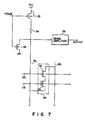
- Fig. 7 is a circuit diagram showing a schematic arrangement when a nonvolatile semiconductor memory of the present invention is applied to an E2PROM.
- Memory cell 30 has a sectional structure similar to that in Fig. 4.
- P-channel MOS transistor 33 for switching and resistor 34 as a load are series-connected between read power source voltage Vcc and read line RL.
- n-channel MOS transistor 35 for switching is connected between read line RL and ground (0 V). Gate electrodes of both switching transistors 33 and 35 are commonly connected.
- Signal Erase whose potential is set at 5 V in the data erase mode and at 0 V in other modes, is supplied to the common node of the gate electrodes.
- the input terminal of sense amplifier 36 is connected to read line RL.
- Resistance Rr is set so as to satisfy the following relationship.
- the potential at read line RL is changed substantially from 5 V to 0 V in each mode. More specifically, when the potential of signal Erase is set at 5 V in the data erase mode, transistor 35 is rendered conductive, and the potential at read line RL is set at 0 V when transistor 35 is rendered conductive. In this case, since transistor 33 is rendered nonconductive, a current does not flow through resistor 34. On the other hand, the potential of signal Erase is 0 V in the modes other than the data erase mode. Since transistors 35 and 33 are rendered nonconductive and conductive, respectively, the potential at read line RL is set at read power source voltage Vcc, i.e., 5 V through resistor 34.
- the voltage ranges at write line WL, selection gate line SG, control gate line CG, and read line RL are respectively set as 0 V to 20 V (high-voltage system), 5 V to 20 V (low- and high-voltage systems), 0 V to 20 V (high-voltage system), and 0 V to 5 V (low-voltage system). More specifically, both and high- and low-voltage systems are present only at selection gate line SG.
- Other lines, i.e., write line WL, control gate line CG, and read line RL are divided into the high- and low-systems. For this reason, the arrangement of peripheral circuits for processing signals from these lines can be considerably simplified. More specifically, in the memory of this embodiment, the peripheral circuits can be divided into the high- and low-systems, thereby simplifying the circuit arrangement.
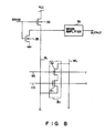
- Fig. 8 is a circuit diagram schematically showing an arrangement of another embodiment according to the present invention.
- p-channel MOS transistor 33 in Fig. 7 is used as a load for read line RL. Note that if an ON resistance of single transistor 33 is Rr, resistance Rr is set so as to satisfy inequality 1 above.
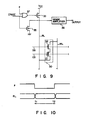
- Fig. 9 is a circuit diagram schematically showing an arrangement of still another embodiment according to the present invention.
- p-channel MOS transistor 33 is used as a load for read line RL as in the embodiment in Fig. 8.
- an output from OR gate 37 is supplied to the gate electrode of transistor 33.
- Signal Erase described above and clock signal ⁇ are supplied to OR gate 37.
- Fig. 11 is a circuit diagram schematically showing an arrangement of still another embodiment according to the present invention.
- p-channel MOS transistor 33 is used as a load circuit for read line RL.
- the gate electrode of p-channel MOS transistor 33 receives an output signal from OR gate 37.
- the voltage of selection gate line SG is not immediately supplied to the gate electrode of selection transistor 32, but the application of voltage is controlled by using AND gate 38 ON/OFF-conrolled by an output signal from OR gate 37.
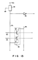
- Fig. 13 is a circuit diagram showing, in detail, sense amplifier 36 used in each embodiment described above together with memory cell 30.
- Circuit 39 connected between read power source voltage Vcc and read line RL corresponds to the circuit including resistor 34 and switching transistors 33 and 35 in Fig. 7, the circuit including switching transistors 33 and 35 in Fig. 8, or the circuit including transistors 33 and 35, and OR gate 37 in Fig. 9.
- a complicated sense amplifier for amplifying a small potential is not necessary for changing the voltage at read line RL from 0 V to 5 V regardless of a type of load connected between read power source voltage Vcc and read line RL.
- an inverter can be used as sense amplifier 36. For this reason, a sense amplifier can be simplified, while an access time can be shortened.
- a nonvolatile semiconductor memory which can be operated at a low voltage and a low power consumption, and can realize simplified, high-speed peripheral circuits such as a sense amplifier.
Landscapes
- Engineering & Computer Science (AREA)
- Microelectronics & Electronic Packaging (AREA)
- Read Only Memory (AREA)
- Non-Volatile Memory (AREA)
Claims (6)
- Mémoire non volatile à semiconducteur, dans laquelle une partie d'une électrode de grille flottante (16) chevauche une couche de diffusion (17) au travers d'un film mince isolant (17), ladite mémoire à semiconducteur comprendant :
un substrat (10) d'un premier type de conductivité ;
des première, seconde et troisième couches de diffusion (11, 12, 13) d'un second type de conductivité opposé audit premier type de conductivité, formées dans ledit substrat (10) ;
une première région de canal (14) formée dans cette partie dudit substrat (10) qui s'étend entre lesdites première et seconde couches de diffusion (11, 12) ;
une seconde région de canal (20) formée dans cette partie dudit substrat (10) qui s'étend entre lesdites seconde et troisième couches de diffusion (12, 13) ;
ladite électrode de grille flottante (16) étant formée au-dessus de ladite première région de canal (14), une partie de ladite électrode de grille flottante (16) étant formée sur ledit film mince isolant (17) formé sur ladite seconde couche de diffusion (12) ;
une électrode de grille de commande (19) formée au-dessus de ladite électrode de grille flottante (16) ;
une électrode de grille (22) formée au-dessus de ladite seconde région de canal (20) ;
une ligne de grille de commande (CG) pour appliquer des tensions prédéterminées à ladite électrode de grille de commande (19), respectivement dans des modes effacement de données, écriture de données et lecture de données ;
une ligne de grille de sélection (SG) pour appliquer des tensions prédéterminées à ladite électrode de grille (22) respectivement dans les modes effacement de données, écriture de données et lecture de données ;
une ligne d'écriture (WL) pour appliquer des tensions prédéterminées à ladite troisième couche de diffusion (13) respectivement dans les modes effacement de données, écriture de données et lecture de données ; et
une ligne de lecture (RL) pour appliquer des tensions prédéterminées à ladite première couche de diffusion (11) respectivement dans les modes effacement de données, écriture de données et lecture de données, dans laquelle :
ladite ligne de grille de commande (CG) applique une première tension à ladite électrode de grille de commande (19) dans le mode effacement de données et applique une seconde tension inférieure à la première tension à ladite électrode de grille de commande (19) dans les modes écriture de données et lecture de données, ladite ligne de grille de sélection (SG) applique la première tension à ladite électrode de grille (22) dans les modes effacement de données et écriture de données et applique une troisième tension qui est inférieure à la première tension et supérieure à la seconde tension à ladite électrode de grille (22) dans le mode lecture de données, ladite ligne d'écriture (WL) applique la seconde tension à ladite troisième couche de diffusion (13) dans le mode effacement de données et applique la première tension à ladite troisième couche de diffusion (13) dans le mode écriture de données et ladite ligne de lecture (RL) applique la seconde tension à ladite première couche de diffusion (11) dans le mode effacement de données et applique la troisième tension à ladite première couche de diffusion (11) dans le mode écriture de données ;
caractérisée en ce que :
ladite ligne d'écriture (WL) applique la seconde tension à ladite troisième couche de diffusion (13) également dans le mode lecture de données et ladite ligne de lecture (RL) applique la troisième tension à ladite première couche de diffusion (11) également dans le mode lecture de données. - Mémoire selon la revendication 1, caractérisée en ce que ladite ligne de lecture (RL) est connectée à une source d'alimentation via un circuit de charge (33, 34) et un signal qui provient de ladite ligne de lecture (RL) est acheminé jusqu'à un amplificateur de lecture (36).
- Mémoire selon la revendication 2, caractérisée en ce que ledit circuit de charge comprend un transistor métal-oxyde-semiconducteur (MOS) (33) qui est normalement rendu conducteur.
- Mémoire selon la revendication 2, caractérisée en ce que ledit circuit de charge comprend un transistor MOS (33) qui est temporairement rendu conducteur en fonction d'un signal d'horloge (φ).
- Mémoire selon la revendication 4, caractérisée en ce que la tension sur ladite ligne de grille de sélection (SG) est appliquée à ladite électrode de grille (22) en synchronisation avec le signal d'horloge (φ).
- Mémoire selon la revendication 2, caractérisée en ce que ledit amplificateur de lecture inclut un inverseur (36).
Applications Claiming Priority (2)
| Application Number | Priority Date | Filing Date | Title |
|---|---|---|---|
| JP2108787A JPH0772996B2 (ja) | 1987-01-31 | 1987-01-31 | 不揮発性半導体メモリ |
| JP21087/87 | 1987-01-31 |
Publications (3)
| Publication Number | Publication Date |
|---|---|
| EP0280883A2 EP0280883A2 (fr) | 1988-09-07 |
| EP0280883A3 EP0280883A3 (en) | 1989-02-08 |
| EP0280883B1 true EP0280883B1 (fr) | 1991-10-23 |
Family
ID=12045090
Family Applications (1)
| Application Number | Title | Priority Date | Filing Date |
|---|---|---|---|
| EP88101335A Expired - Lifetime EP0280883B1 (fr) | 1987-01-31 | 1988-01-29 | Equipement de mémoire permanente à semi-conducteur |
Country Status (5)
| Country | Link |
|---|---|
| US (1) | US4912749A (fr) |
| EP (1) | EP0280883B1 (fr) |
| JP (1) | JPH0772996B2 (fr) |
| KR (1) | KR900009176B1 (fr) |
| DE (1) | DE3865702D1 (fr) |
Families Citing this family (18)
| Publication number | Priority date | Publication date | Assignee | Title |
|---|---|---|---|---|
| US5138575A (en) * | 1988-12-19 | 1992-08-11 | Fujitsu Limited | Electricaly erasable and programmable read only memory with a discharge device |
| JPH0738274B2 (ja) * | 1988-12-22 | 1995-04-26 | 株式会社東芝 | 不揮発性半導体メモリシステム |
| JP2529885B2 (ja) * | 1989-03-10 | 1996-09-04 | 工業技術院長 | 半導体メモリ及びその動作方法 |
| JP2807256B2 (ja) * | 1989-03-17 | 1998-10-08 | 株式会社東芝 | 不揮発性半導体メモリ |
| FR2650109B1 (fr) * | 1989-07-20 | 1993-04-02 | Gemplus Card Int | Circuit integre mos a tension de seuil ajustable |
| JPH04123471A (ja) | 1990-09-14 | 1992-04-23 | Oki Electric Ind Co Ltd | 半導体記憶装置のデータ書込みおよび消去方法 |
| KR940005695B1 (ko) * | 1990-12-19 | 1994-06-22 | 삼성전자 주식회사 | 불휘발성 기억소자의 로우 디코더 회로 |
| KR930011000A (ko) * | 1991-11-29 | 1993-06-23 | 김광호 | 이이피롬 장치 |
| US5898619A (en) * | 1993-03-01 | 1999-04-27 | Chang; Ko-Min | Memory cell having a plural transistor transmission gate and method of formation |
| GB2304947B (en) * | 1995-08-31 | 2000-02-23 | Motorola Ltd | Electrically programmable memory, method of programming and method of reading |
| US5736891A (en) * | 1996-01-11 | 1998-04-07 | International Business Machines Corporation | Discharge circuit in a semiconductor memory |
| FR2770326B1 (fr) * | 1997-10-28 | 2001-12-28 | Sgs Thomson Microelectronics | Procede d'ecriture dans une memoire non volatile modifiable electriquement |
| EP0936629B1 (fr) * | 1998-02-12 | 2006-09-13 | Infineon Technologies AG | EEPROM et procédé de commande d'une mémoire EEPROM |
| DE102004042105A1 (de) | 2004-08-30 | 2006-03-09 | Infineon Technologies Ag | ROM-Speicher |
| US8320191B2 (en) | 2007-08-30 | 2012-11-27 | Infineon Technologies Ag | Memory cell arrangement, method for controlling a memory cell, memory array and electronic device |
| JP5191834B2 (ja) * | 2008-08-12 | 2013-05-08 | セイコーインスツル株式会社 | 半導体不揮発性記憶装置 |
| JP6751013B2 (ja) * | 2016-12-27 | 2020-09-02 | 旭化成エレクトロニクス株式会社 | 温度特性調整回路 |
| US11049565B2 (en) * | 2018-04-23 | 2021-06-29 | Micron Technology, Inc. | Non-volatile memory devices and systems with volatile memory features and methods for operating the same |
Family Cites Families (15)
| Publication number | Priority date | Publication date | Assignee | Title |
|---|---|---|---|---|
| US4375087C1 (en) * | 1980-04-09 | 2002-01-01 | Hughes Aircraft Co | Electrically erasable programmable read-only memory |
| JPS5747517A (en) * | 1980-09-04 | 1982-03-18 | Ishikawajima Harima Heavy Ind Co Ltd | Method and apparatus for controlling rolling speed of mandrel mill |
| JPS5834628A (ja) * | 1981-08-24 | 1983-03-01 | Hitachi Ltd | Mosインバ−タ回路 |
| US4558344A (en) * | 1982-01-29 | 1985-12-10 | Seeq Technology, Inc. | Electrically-programmable and electrically-erasable MOS memory device |
| JPS58161198A (ja) * | 1982-03-19 | 1983-09-24 | Ricoh Co Ltd | 半導体メモリ |
| JPS5955071A (ja) * | 1982-09-24 | 1984-03-29 | Hitachi Micro Comput Eng Ltd | 不揮発性半導体装置 |
| JPS60182174A (ja) * | 1984-02-28 | 1985-09-17 | Nec Corp | 不揮発性半導体メモリ |
| US4628487A (en) * | 1984-08-14 | 1986-12-09 | Texas Instruments Incorporated | Dual slope, feedback controlled, EEPROM programming |
| US4611309A (en) * | 1984-09-24 | 1986-09-09 | Advanced Micro Devices, Inc. | Non-volatile dynamic RAM cell |
| US4729115A (en) * | 1984-09-27 | 1988-03-01 | International Business Machines Corporation | Non-volatile dynamic random access memory cell |
| EP0183235B1 (fr) * | 1984-11-26 | 1993-10-06 | Kabushiki Kaisha Toshiba | Dispositif de mémoire semi-conductrice non-volatile |
| JPH0746515B2 (ja) * | 1984-12-28 | 1995-05-17 | 日本電気株式会社 | デコ−ダ回路 |
| JPH0783064B2 (ja) * | 1985-01-18 | 1995-09-06 | 株式会社日立製作所 | 半導体記憶装置 |
| US4752912A (en) * | 1985-05-14 | 1988-06-21 | Xicor, Inc. | Nonvolatile electrically alterable memory and method |
| US4599706A (en) * | 1985-05-14 | 1986-07-08 | Xicor, Inc. | Nonvolatile electrically alterable memory |
-
1987
- 1987-01-31 JP JP2108787A patent/JPH0772996B2/ja not_active Expired - Lifetime
-
1988
- 1988-01-28 US US07/149,606 patent/US4912749A/en not_active Expired - Lifetime
- 1988-01-29 EP EP88101335A patent/EP0280883B1/fr not_active Expired - Lifetime
- 1988-01-29 DE DE8888101335T patent/DE3865702D1/de not_active Expired - Lifetime
- 1988-01-29 KR KR1019880000784A patent/KR900009176B1/ko not_active IP Right Cessation
Also Published As
| Publication number | Publication date |
|---|---|
| JPS63188896A (ja) | 1988-08-04 |
| DE3865702D1 (de) | 1991-11-28 |
| EP0280883A3 (en) | 1989-02-08 |
| KR880009379A (ko) | 1988-09-15 |
| EP0280883A2 (fr) | 1988-09-07 |
| KR900009176B1 (ko) | 1990-12-24 |
| US4912749A (en) | 1990-03-27 |
| JPH0772996B2 (ja) | 1995-08-02 |
Similar Documents
| Publication | Publication Date | Title |
|---|---|---|
| US4870615A (en) | Nonvolatile floating gate semiconductor memory device | |
| EP0280883B1 (fr) | Equipement de mémoire permanente à semi-conducteur | |
| EP0467928B1 (fr) | Cellules de memoire vive non volatile amelioree utilisant deux elements differentiels de memoire non volatile pouvant etre desaccouples | |
| US4435786A (en) | Self-refreshing memory cell | |
| US5099143A (en) | Dual voltage supply circuit with multiplier-controlled transistor | |
| EP0586473B1 (fr) | Cellule d'interconnexion remanente effacable et programmable | |
| US5777926A (en) | Row decoder circuit for PMOS non-volatile memory cell which uses channel hot electrons for programming | |
| JPH02168497A (ja) | 不揮発性半導体メモリシステム | |
| US6266276B1 (en) | Non-volatile semiconductor memory device and internal operation method for said non-volatile semiconductor memory device | |
| EP0866466A2 (fr) | Méthode de polarisation pour réduction de tension et amélioration de fiabilité dans des cellules de mémoire EEPROM | |
| US5025417A (en) | Semiconductor memory device capable of preventing data of non-selected memory cell from being degraded | |
| EP0387889B1 (fr) | Mémoire rémanente en semi-conducteur | |
| JPH0323999B2 (fr) | ||
| US7042763B1 (en) | Programming method for nonvolatile memory cell | |
| EP0376290B1 (fr) | Dispositif de mémoire non volatile à semi-conducteurs capable d'empêcher une erreur de lecture due à un état de sur effacement | |
| KR100432442B1 (ko) | 자기 증폭 다이내믹 메모리 셀을 갖춘 메모리 셀 어레이를동작시키기 위한 방법 | |
| US7020027B1 (en) | Programming method for nonvolatile memory cell | |
| JPS6027118B2 (ja) | 半導体メモリ装置 | |
| US4423491A (en) | Self-refreshing memory cell | |
| JP2648099B2 (ja) | 不揮発性半導体メモリ装置およびそのデータ消去方法 | |
| JP2875068B2 (ja) | バイアス電位発生回路 | |
| JP2553290B2 (ja) | 半導体集積回路 | |
| EP0311146A1 (fr) | Cellulle de mémoire à autogénération | |
| CA1189972A (fr) | Cellule de memoire a auto-regeneration | |
| JPH0645564A (ja) | 不揮発性半導体メモリ |
Legal Events
| Date | Code | Title | Description |
|---|---|---|---|
| PUAI | Public reference made under article 153(3) epc to a published international application that has entered the european phase |
Free format text: ORIGINAL CODE: 0009012 |
|
| 17P | Request for examination filed |
Effective date: 19880226 |
|
| AK | Designated contracting states |
Kind code of ref document: A2 Designated state(s): DE FR GB |
|
| PUAL | Search report despatched |
Free format text: ORIGINAL CODE: 0009013 |
|
| AK | Designated contracting states |
Kind code of ref document: A3 Designated state(s): DE FR GB |
|
| 17Q | First examination report despatched |
Effective date: 19900914 |
|
| GRAA | (expected) grant |
Free format text: ORIGINAL CODE: 0009210 |
|
| AK | Designated contracting states |
Kind code of ref document: B1 Designated state(s): DE FR GB |
|
| REF | Corresponds to: |
Ref document number: 3865702 Country of ref document: DE Date of ref document: 19911128 |
|
| ET | Fr: translation filed | ||
| PLBE | No opposition filed within time limit |
Free format text: ORIGINAL CODE: 0009261 |
|
| STAA | Information on the status of an ep patent application or granted ep patent |
Free format text: STATUS: NO OPPOSITION FILED WITHIN TIME LIMIT |
|
| 26N | No opposition filed | ||
| REG | Reference to a national code |
Ref country code: GB Ref legal event code: IF02 |
|
| PGFP | Annual fee paid to national office [announced via postgrant information from national office to epo] |
Ref country code: GB Payment date: 20070124 Year of fee payment: 20 |
|
| PGFP | Annual fee paid to national office [announced via postgrant information from national office to epo] |
Ref country code: DE Payment date: 20070125 Year of fee payment: 20 |
|
| REG | Reference to a national code |
Ref country code: GB Ref legal event code: PE20 |
|
| PGFP | Annual fee paid to national office [announced via postgrant information from national office to epo] |
Ref country code: FR Payment date: 20070109 Year of fee payment: 20 |
|
| PG25 | Lapsed in a contracting state [announced via postgrant information from national office to epo] |
Ref country code: GB Free format text: LAPSE BECAUSE OF EXPIRATION OF PROTECTION Effective date: 20080128 |