EP0268472B1 - Statische Induktionstransistoren mit isoliertem Gatter in einer eingeschnittenen Stufe und Verfahren zu deren Herstellung - Google Patents
Statische Induktionstransistoren mit isoliertem Gatter in einer eingeschnittenen Stufe und Verfahren zu deren Herstellung Download PDFInfo
- Publication number
- EP0268472B1 EP0268472B1 EP87310185A EP87310185A EP0268472B1 EP 0268472 B1 EP0268472 B1 EP 0268472B1 EP 87310185 A EP87310185 A EP 87310185A EP 87310185 A EP87310185 A EP 87310185A EP 0268472 B1 EP0268472 B1 EP 0268472B1
- Authority
- EP
- European Patent Office
- Prior art keywords
- mask material
- static induction
- insulated gate
- side wall
- drain
- Prior art date
- Legal status (The legal status is an assumption and is not a legal conclusion. Google has not performed a legal analysis and makes no representation as to the accuracy of the status listed.)
- Expired - Lifetime
Links
Images


Classifications
-
- H—ELECTRICITY
- H10—SEMICONDUCTOR DEVICES; ELECTRIC SOLID-STATE DEVICES NOT OTHERWISE PROVIDED FOR
- H10D—INORGANIC ELECTRIC SEMICONDUCTOR DEVICES
- H10D30/00—Field-effect transistors [FET]
- H10D30/01—Manufacture or treatment
- H10D30/012—Manufacture or treatment of static induction transistors [SIT], e.g. permeable base transistors [PBT]
-
- H—ELECTRICITY
- H10—SEMICONDUCTOR DEVICES; ELECTRIC SOLID-STATE DEVICES NOT OTHERWISE PROVIDED FOR
- H10D—INORGANIC ELECTRIC SEMICONDUCTOR DEVICES
- H10D30/00—Field-effect transistors [FET]
- H10D30/202—FETs having static field-induced regions, e.g. static-induction transistors [SIT] or permeable base transistors [PBT]
-
- H—ELECTRICITY
- H10—SEMICONDUCTOR DEVICES; ELECTRIC SOLID-STATE DEVICES NOT OTHERWISE PROVIDED FOR
- H10D—INORGANIC ELECTRIC SEMICONDUCTOR DEVICES
- H10D62/00—Semiconductor bodies, or regions thereof, of devices having potential barriers
- H10D62/10—Shapes, relative sizes or dispositions of the regions of the semiconductor bodies; Shapes of the semiconductor bodies
- H10D62/17—Semiconductor regions connected to electrodes not carrying current to be rectified, amplified or switched, e.g. channel regions
- H10D62/213—Channel regions of field-effect devices
- H10D62/221—Channel regions of field-effect devices of FETs
- H10D62/228—Channel regions of field-effect devices of FETs having delta-doped channels
-
- H—ELECTRICITY
- H10—SEMICONDUCTOR DEVICES; ELECTRIC SOLID-STATE DEVICES NOT OTHERWISE PROVIDED FOR
- H10D—INORGANIC ELECTRIC SEMICONDUCTOR DEVICES
- H10D84/00—Integrated devices formed in or on semiconductor substrates that comprise only semiconducting layers, e.g. on Si wafers or on GaAs-on-Si wafers
- H10D84/80—Integrated devices formed in or on semiconductor substrates that comprise only semiconducting layers, e.g. on Si wafers or on GaAs-on-Si wafers characterised by the integration of at least one component covered by groups H10D12/00 or H10D30/00, e.g. integration of IGFETs
- H10D84/82—Integrated devices formed in or on semiconductor substrates that comprise only semiconducting layers, e.g. on Si wafers or on GaAs-on-Si wafers characterised by the integration of at least one component covered by groups H10D12/00 or H10D30/00, e.g. integration of IGFETs of only field-effect components
-
- H—ELECTRICITY
- H10—SEMICONDUCTOR DEVICES; ELECTRIC SOLID-STATE DEVICES NOT OTHERWISE PROVIDED FOR
- H10P—GENERIC PROCESSES OR APPARATUS FOR THE MANUFACTURE OR TREATMENT OF DEVICES COVERED BY CLASS H10
- H10P14/00—Formation of materials, e.g. in the shape of layers or pillars
- H10P14/60—Formation of materials, e.g. in the shape of layers or pillars of insulating materials
- H10P14/61—Formation of materials, e.g. in the shape of layers or pillars of insulating materials using masks
-
- H—ELECTRICITY
- H10—SEMICONDUCTOR DEVICES; ELECTRIC SOLID-STATE DEVICES NOT OTHERWISE PROVIDED FOR
- H10W—GENERIC PACKAGES, INTERCONNECTIONS, CONNECTORS OR OTHER CONSTRUCTIONAL DETAILS OF DEVICES COVERED BY CLASS H10
- H10W20/00—Interconnections in chips, wafers or substrates
- H10W20/01—Manufacture or treatment
- H10W20/031—Manufacture or treatment of conductive parts of the interconnections
- H10W20/069—Manufacture or treatment of conductive parts of the interconnections by forming self-aligned vias or self-aligned contact plugs
Definitions
- This invention relates to a step-cut insulated gate static induction transistor capable of carrying out high-speed switching, a high-speed and low power step-cut insulated gate static induction transistor integrated circuit, and method of manufacturing the same.
- Insulated gate transistors for high frequency amplification and integrated circuits have been heretofore used but have a disadvantage that the drivability is small.
- a complementary metal-oxide-semiconductor transistor integrated circuit (C-MOS) has been known as an application of an insulated gate transistor.
- this circuit (C-MOS) operates at low dissipation power but operates at low switching speed, because of small drivability
- an insulated gate static induction transistor for example, see Japanese Patent Application No. 1756/1977
- a step-cut insulated gate static induction transistor for example, see Japanese Patent Application No. 13,707/1977.
- the insulated gate static induction transistor is designed so that the depletion layer spread from the drain region reaches the source region. So, a current flowing from source to drain is controlled not only by the gate voltage but also by the drain voltage and the current flows into not only an interface between a semiconductor and an insulator but a substrate. Therefore, the insulated gate static induction transistor has non-saturating current-voltage characteristics and has large drivability.
- the step-cut insulated gate static induction transistor has a channel formed depthwise of a semiconductor substrate, thus providing a good controllability for a channel length and a gate length, and said transistor is well suited for shortening a channel to improve its drivability.
- the step-cut insulated gate static induction transistor is able to increase its drivability and decrease a parastic capacitance and therefore exhibits an excellent performance as a high speed switching transistor and a high-speed and low power integrated circuit.
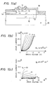
- FIG.1 (a) shows an example of a construction in section of a conventional step-cut insulated gate static induction transistor.
- 10 designates a semiconductor substrate, a main surface of which is partly provided with a U-shaped groove.
- a drain region 11, a channel region 13 and a source region 12 are provided in said order depthwise from the main surface along the side wall of the U-shaped groove, and a drain electrode 11' is connected to the drain region 11.
- a source electrode, which is not shown, is provided vertically as viewed from the paper surface.
- the drain region 11 and the source region 12 have the impurity concentration of the order 10 18 of to 10 21 cm- 3 , the conductivity type of which is shown as P type but N type can be used.
- the region 11 can be used as a source region and the region 12 used as a drain region.
- the channel region 13 has the impurity concentration of the order of 10 12 to loll cm- 3 , the conductivity type of which can be of the same as or opposite to that of the drain region 11 and the source region 12, and a multi-layered construction can be also employed.
- the impurity concentration as well as the depth of the aforesaid U-shaped groove are determined so that a depletion layer spread from the drain region 11 reaches the source region 12 at least a part of the operating condition thereof.
- a gate electrode 14' formed of metal, polycrystalline silicon or the like.
- 15 designates a field oxide film. Since a conventional step-cut insulated gate static conduction transistor as shown in FIG. 1 (a) is formed depthwise with respect to a semiconductor substrate. dimensions of a transistor can be controlled with precision of deposition and etching providing a good controllability for the channel length and gate length and being well suited for shortening the channel to improve drivability. Accordingly, such a transistor as noted above has a large drivability and can decrease a parastic capac- tance and therefore exhibits an excellent performance as a high speed switching transistor and a high speed low power integrated circuit.
- An epitaxial layer 22 constituting a channel is grown on a semiconductor substrate 21 used as a drain, a channel impurity is introduced by thermal diffusion or ion implantation and thereafter a U-shaped groove is formed in a part of a main surface of the semiconductor substrate by anisotropic plasma etching or the like.
- a conventional photolithography and a selective oxidation are used to form a field oxid film 23 and windows, which are provided in a part of a main surface of a semiconductor substrate and are including at a part of the side wall of a U-shaped groove to form a gate oxide film 24.
- a polycrystalline silicon 25 constituting a gate electrode is deposited, which is subjected to etching by a conventional photolithography so as to have it remained on a gate oxide film of the side wall of a U-shaped groove, and thereafter a source region 26 is formed by thermal diffusion or ion implantation.
- a passivation film 27 is deposited and contact hole is opened to form a drain electrode 21 a gate electrode 25' and a source electrode 26'.
- the impurity concentration of the aforesaid drain region 21 and source region 26 is of the order of 10 18 to 10 21 cm- 3 .
- the conductive type can be of either P type or N type, and the 21 can be used as a source region and the 26 as a drain region conversely to the former.
- the impurity concentration of the channel region 22 is of the order of 10 12 to 10 16 cm- 3 , and the conductive type thereof can be the same as or opposite to that of the aforementioned drain region and source region, a multi-layered construction being possibly used.
- the thickness of the gate oxide film 24 is set to be of the order of 100 to 1,000 ⁇ , and the gate electrode is ordinarily formed of polycrystalline silicon or the like, the thickness being of the order of 1000 A to 1 am.
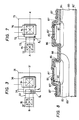
- FIG. 3 shows an example of a plan construction of a conventional step-cut insulated gate static induction transistor, which corresponds to the fabrication process shown in FIG. 2.
- 31 designates a side wall of a U-shaped groove, 32 a window provided by selective oxidation, 33 a gate electrode of a polycrystalline silicon, 34 and 35 a drain contact hole and a gate contact hole, respectively, and 36 and 37 a drain electrode and a gate electrode, respectively.
- the section of B-B' is shown in FIG. 2(d).
- lb and Ic denote mask alignment margins with respect to the photolithography of the FIG. 2 processes (b) and (c), the margin being normally designed approximately 0.1 to 2 ⁇ m.
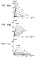
- FIGS. 4 (a) to (c) An example of the drain current-drain voltage characteristics of a transistor different in mask alignment margin ic is shown in FIGS. 4 (a) to (c).
- the channel length is approximately 0.5 ⁇ m; the dosage of the channel impurity is approximately 1.5 x 1013 cm-2 ; and the thickness of the gate oxide film is approximately 250 ⁇ , the mask alignment margin îc being 0 um in the (a), and 1 ⁇ m and 2 ⁇ m in the (b) and (c), respectively.
- the (a) there exhibits the unsaturated type current-voltage characteristic, the drivability is large and the characteristic of the step-cut insulated gate static induction transistor is conspicuous but there gives rise to a disadvantage that yield is poor.
- the effective channel length becomes extended, deteriorating the drivability.
- FIG. 1 (b) shows an example of the drain current-drain voltage characteristics of a conventional step-cut insulated gate static induction transistor so designed that the channel length is approximately 0.5 ⁇ m, the dosage of channel impurity is approximately 2 x 1013 cm-2, and the thickness of the gate oxide film is approximately 250 ⁇ .
- FIG. 1 (c) shows an example of the drain current - drain voltage characteristics of a conventional step-cut insulated gate static induction transistor so designed that the channel length is approximately 0.5 ⁇ m, the dosage of channel impurity is approximately 6 x 10 13 cm- 2 , and the thickness of the gate oxide film is approximately 250 ,4.
- a leak current at the off state was improved but drivability is sacrificed to some extent because the static induction effect on the drain side became hard to extend to the source side, and the threshold voltage is increased.
- An object of the present invention is to provide a method of manufacturing a step-cut insulated gate static induction transistor wherein the above described problem of mask alignment in formation of the gate oxide film and the gate electrode can be avoided.
- a method of manufacturing a step-cut insulated gate static induction transistor characterized by the following sequence of steps:
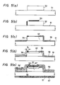
- FIG. 5 shows one embodiment of the fabrication process, according to this invention, step-cut insulated gate static induction transistor shown in FIG. 1.
- An epitaxial layer 52 constituting a channel is grown on a semiconductor substrate 51 used as a drain, a channel impurity is introduced therein by thermal diffusion or ion implantation and thereafter a U-shaped groove is formed in a main surface of a semiconductor substrate by anisotropic plasma etching or the like.
- a mask material 53 for selective oxidation is deposited, and conventional photolithography and anisotropic plasma etching are combined to leave mask material on a region as a source of the main surface of a semiconductor substrate and on a region as a gate of the side wall of a U-shaped groove.
- a selective oxidation is used to form a field oxide film 55, and at the same time a window is formed in a region as a source of the main surface of a semiconductor substrate and in a region as a gate of the side wall of a U-shaped groove to form a gate oxide film 54.
- a polycrystalline silicon 56 constituting a gate electrode is deposited and then subjected to etching so as to be left on a gate oxide film 54 of the side wall of a U-shaped groove by conventional photolithography after which a source region 57 is formed by thermal diffusion or ion implantation.
- a passivation film 58 is deposited and a contact hole is made to form a drain electrode 51', a gate electrode 56' and a source electrode 57'.
- the impurity concentration of a drain region 51 and a source region 57 is of the order of 10 18 to 10 21 cm- 3 .
- the conductivity type can be either P type or N type, and the 51 can be used as a source region and the 57 as a drain region.
- the impurity concentration of the channel region 52 is of the order of 10 12 to 10 16 cm -3 , and the conductivity type thereof can be the same as or opposite to that of said drain region 51 and source region 57, and a multi-layer construction can be employed.
- the impurity concentration as well as the depth of the U-shaped groove are determined so that a depletion layer spread from the drain region reaches the source region.
- the thickness of the gate oxide film 54 is set to approximately 100 to 1,000 ,4.
- a gate oxide film which most influences upon the characteristic of the device can be self-adjustably formed only on the side wall of the U-shaped groove, and therefore, a step-cut insulated gate static induction transistor can be obtained which has excellent in reproducibility and reliability and has an drain current - drain voltage characteristic such as in FIG. 4 (a).
- FIG. 6 further shows in detail the step of forming the mask material 53 shown in FIG. 5 (b).
- An epitaxial layer 62 constituting a channel is grown on a semiconductor substrate 61 used as a drain, a channel impurity is introduced therein by thermal diffusion or ion implantation and thereafter a U-shaped groove is formed in a part of the surface of a semiconductor by anisotropic plasma etching or the like.
- a polycrystalline silicon 64 constituting a mask material for etching of silicon nitride film 63 and a silicon nitride film 63 constituting a mask material for selective oxidation is continuously deposited by CVD method or the like.
- a polycrystalline silicon 64 on a region as a source of the main surface of a semiconductor substrate and on a region as a gate of the side wall of the U-shaped groove.
- the polycrystalline silicon 64 is used as a mask material to apply etching to a silicon nitride film 63 constituting a mask material for selective oxidation.
- the silicon nitride film which is the mask material for selective oxidation can be self-adjustably formed only on the side wall of the U-shaped groove.
- the silicon nitride film can be directly subjected to anisotropic etching but according to this method, etching of a silicon nitride film can be effected by wet etching such as boiled phosphoric acid, etc., without damage.
- FIG. 7 One example of a plane construction of an step-cut insulated gate static induction transistor corresponding to the fabrication process shown in FIGS. 5 and 6 is shown in FIG. 7.
- 71 designates a side wall of a U-shaped groove, 72 a window caused by selective oxidation constituting an active area, 73 a gate electrode of a polycrystalline silicon, 74 and 75 a drain contact hole and a gate contact hole, respectively, and 76 and 77 a drain electrode and a gate electrode, respectively.
- the section taken by A-A' is shown in FIG. 5 (e).
- îd denotes the mask alignment margin with respect to the photolithography in the step (d) shown in FIG. 5, the margin being normally set to approximately 0.1 ⁇ m to 2 /1 .m.
- this part is a thick field oxide film, and so even if it is superposed by the gate electrode, no significant influence is extended to device characteristic.
- FIG. 8 One example of a sectional construction of a inverter gate in the case where the step-cut insulated gate static induction transistor is applied to a complementary metal-oxide-semiconductor transistor integrated circuit is shown in FIG. 8.
- 80 designates a semiconductor substrate, and the main surface thereof is partly formed with a U-shaped groove.
- 81 designates an N + drain region, 82 a P + drain region, 83 an N + source region, and 84 a P + source region, these regions having the impurity concentration of approximately 10 18 to 10 21 cm- 3 .
- 85 designates a P channel region and 86 an N channel region, these regions having the impurity concentration of approximately 10 12 to 10 16 cm- 3 .
- the impurity concentration as well as the depth of the U-shaped groove are determined so that a depletion layer spread from the drain region reaches the source region.
- 87 designates a gate insulator such as an oxide film which has a thickness of approximately 100 to 1,000 ,4, 87' a gate electrode, and 88 a field oxide film.
- 89 designates a P well for separating a P channel transistor from an N channel transistor.
- the gate electrode 87' comprises a logical input while the drain electrodes 81' and 82' comprise a logical output, a power- supplied voltage is applied to source electrodes connected to the source regions 83 and 84, respectively.
- the logical input is in a high level, the N channel transistor assumes an on state while the P channel transistor assumes an off state, and therefore the logical output is a low level. The same is true for the reversal case.
- Such an integrated circuit can be manufactured nearly similarly to the fabrication process shown in FIG. 5 except the construction of the substrate, thus providing a complementary metal-oxide-semiconductor transistor integrated circuit which has a good reproducibility and reliability and has high speed and low power.
- a propagation delay time of 430 psec is obtained at a dissipation power of 10 mW, by a ring oscillator of the complementary metal-oxide-semiconductor transistor integrated circuit shown in FIG. 8.
- the present invention improves the disadvantages encountered in the conventional fabrication process of step-cut insulated gate static induction transistor, whereby a gate oxide film and a gate electrode can be self-adjustably formed only on the side wall of the U-shaped groove. Accordingly, the step-cut insulated gate static induction transistor which can effect high speed switching and the high speed and low power step-cut insulated gate static induction transistor integrated circuit can be manufactured with good reproducibility and reliability, thus providing a great industrial value.
Landscapes
- Junction Field-Effect Transistors (AREA)
- Insulated Gate Type Field-Effect Transistor (AREA)
- Metal-Oxide And Bipolar Metal-Oxide Semiconductor Integrated Circuits (AREA)
Claims (3)
Priority Applications (2)
| Application Number | Priority Date | Filing Date | Title |
|---|---|---|---|
| EP92101661A EP0481965B1 (de) | 1986-11-19 | 1987-11-18 | Verfahren zur Herstellung der Statischen Induktionstransistoren mit isoliertem Gatter in einer eingeschnitteten Stufe |
| EP93101675A EP0547030B1 (de) | 1986-11-19 | 1987-11-18 | Statische Induktiontransistoren mit isoliertem Gatter in einer eingeschnittenen Stufe und Verfahren zu deren Herstellung |
Applications Claiming Priority (8)
| Application Number | Priority Date | Filing Date | Title |
|---|---|---|---|
| JP273935/86 | 1986-11-19 | ||
| JP27393586A JPS63128675A (ja) | 1986-11-19 | 1986-11-19 | 切り込み型絶縁ゲ−ト静電誘導トランジスタ |
| JP273934/86 | 1986-11-19 | ||
| JP27393486A JPS63128674A (ja) | 1986-11-19 | 1986-11-19 | 切り込み型絶縁ゲ−ト静電誘導トランジスタ |
| JP27675486A JPS63131583A (ja) | 1986-11-21 | 1986-11-21 | 切り込み型絶縁ゲ−ト静電誘導トランジスタの製造方法 |
| JP27675586A JPS63131584A (ja) | 1986-11-21 | 1986-11-21 | 切り込み型絶縁ゲ−ト静電誘導トランジスタの製造方法 |
| JP276755/86 | 1986-11-21 | ||
| JP276754/86 | 1986-11-21 |
Related Child Applications (4)
| Application Number | Title | Priority Date | Filing Date |
|---|---|---|---|
| EP92101661.4 Division-Into | 1987-11-10 | ||
| EP92101661A Division EP0481965B1 (de) | 1986-11-19 | 1987-11-18 | Verfahren zur Herstellung der Statischen Induktionstransistoren mit isoliertem Gatter in einer eingeschnitteten Stufe |
| EP93101675A Division EP0547030B1 (de) | 1986-11-19 | 1987-11-18 | Statische Induktiontransistoren mit isoliertem Gatter in einer eingeschnittenen Stufe und Verfahren zu deren Herstellung |
| EP93101675.2 Division-Into | 1993-02-04 |
Publications (3)
| Publication Number | Publication Date |
|---|---|
| EP0268472A2 EP0268472A2 (de) | 1988-05-25 |
| EP0268472A3 EP0268472A3 (en) | 1988-08-17 |
| EP0268472B1 true EP0268472B1 (de) | 1994-02-02 |
Family
ID=27479007
Family Applications (4)
| Application Number | Title | Priority Date | Filing Date |
|---|---|---|---|
| EP95114168A Expired - Lifetime EP0690513B1 (de) | 1986-11-19 | 1987-11-10 | Statische Induktionstransistoren mit isoliertem Gatter in einer eingeschnittenen Stufe und Verfahren zu deren Herstellung |
| EP92101661A Expired - Lifetime EP0481965B1 (de) | 1986-11-19 | 1987-11-18 | Verfahren zur Herstellung der Statischen Induktionstransistoren mit isoliertem Gatter in einer eingeschnitteten Stufe |
| EP87310185A Expired - Lifetime EP0268472B1 (de) | 1986-11-19 | 1987-11-18 | Statische Induktionstransistoren mit isoliertem Gatter in einer eingeschnittenen Stufe und Verfahren zu deren Herstellung |
| EP93101675A Expired - Lifetime EP0547030B1 (de) | 1986-11-19 | 1987-11-18 | Statische Induktiontransistoren mit isoliertem Gatter in einer eingeschnittenen Stufe und Verfahren zu deren Herstellung |
Family Applications Before (2)
| Application Number | Title | Priority Date | Filing Date |
|---|---|---|---|
| EP95114168A Expired - Lifetime EP0690513B1 (de) | 1986-11-19 | 1987-11-10 | Statische Induktionstransistoren mit isoliertem Gatter in einer eingeschnittenen Stufe und Verfahren zu deren Herstellung |
| EP92101661A Expired - Lifetime EP0481965B1 (de) | 1986-11-19 | 1987-11-18 | Verfahren zur Herstellung der Statischen Induktionstransistoren mit isoliertem Gatter in einer eingeschnitteten Stufe |
Family Applications After (1)
| Application Number | Title | Priority Date | Filing Date |
|---|---|---|---|
| EP93101675A Expired - Lifetime EP0547030B1 (de) | 1986-11-19 | 1987-11-18 | Statische Induktiontransistoren mit isoliertem Gatter in einer eingeschnittenen Stufe und Verfahren zu deren Herstellung |
Country Status (3)
| Country | Link |
|---|---|
| US (1) | US5115287A (de) |
| EP (4) | EP0690513B1 (de) |
| DE (4) | DE3752273T2 (de) |
Families Citing this family (5)
| Publication number | Priority date | Publication date | Assignee | Title |
|---|---|---|---|---|
| EP0690513B1 (de) * | 1986-11-19 | 1999-05-06 | Research Development Corporation of Japan | Statische Induktionstransistoren mit isoliertem Gatter in einer eingeschnittenen Stufe und Verfahren zu deren Herstellung |
| US5266523A (en) * | 1991-11-14 | 1993-11-30 | Micron Technology, Inc. | Method of forming self-aligned contacts using the local oxidation of silicon |
| DE19503641A1 (de) * | 1995-02-06 | 1996-08-08 | Forschungszentrum Juelich Gmbh | Schichtstruktur mit einer Silicid-Schicht, sowie Verfahren zur Herstellung einer solchen Schichtstruktur |
| US6341144B1 (en) * | 1996-09-20 | 2002-01-22 | At&T Corp. | Video coder providing implicit coefficient prediction and scan adaptation for image coding and intra coding of video |
| US6977406B2 (en) | 2001-04-27 | 2005-12-20 | National Institute Of Information And Communications Technology, Incorporated Administrative Agency | Short channel insulated-gate static induction transistor and method of manufacturing the same |
Citations (1)
| Publication number | Priority date | Publication date | Assignee | Title |
|---|---|---|---|---|
| US4541166A (en) * | 1980-09-24 | 1985-09-17 | Semiconductor Energy Laboratory Co. | Method of making semiconductor deivce using a conductive layer as mask |
Family Cites Families (14)
| Publication number | Priority date | Publication date | Assignee | Title |
|---|---|---|---|---|
| USRE29971E (en) * | 1971-07-31 | 1979-04-17 | Zaidan Hojin Hondotai Kenkyn Shinkokai | Field effect semiconductor device having an unsaturated triode vacuum tube characteristic |
| JPS53142189A (en) * | 1977-05-17 | 1978-12-11 | Matsushita Electronics Corp | Insulating gate type field effect transistor |
| JPS54125986A (en) * | 1978-03-23 | 1979-09-29 | Handotai Kenkyu Shinkokai | Semiconductor including insulated gate type transistor |
| GB2100173B (en) * | 1978-04-24 | 1983-06-02 | Yoshino Kogyosho Co Ltd | Apparatus for removing injection-moulded parisons |
| US4427990A (en) * | 1978-07-14 | 1984-01-24 | Zaidan Hojin Handotai Kenkyu Shinkokai | Semiconductor photo-electric converter with insulated gate over p-n charge storage region |
| JPS5565463A (en) * | 1978-11-13 | 1980-05-16 | Semiconductor Res Found | Semiconductor device |
| JPS55133574A (en) * | 1979-04-05 | 1980-10-17 | Nec Corp | Insulated gate field effect transistor |
| JPS5735591A (en) * | 1980-08-12 | 1982-02-26 | Mochida Pharmaceut Co Ltd | Novel pyrimidine derivative |
| GB2103879B (en) * | 1981-08-19 | 1985-04-11 | Secr Defence | Method for producing a vertical channel transistor |
| JPS5856270A (ja) * | 1981-09-30 | 1983-04-02 | Fujitsu Ltd | 滋気デイスク装置 |
| JPS59186371A (ja) * | 1983-04-07 | 1984-10-23 | Fuji Xerox Co Ltd | 半導体装置 |
| JPS6028394A (ja) * | 1983-07-26 | 1985-02-13 | Matsushita Electric Ind Co Ltd | ビデオ再生装置 |
| FR2555816B1 (fr) * | 1983-11-25 | 1986-04-11 | Thomson Csf | Transistor a effet de champ a structure verticale |
| EP0690513B1 (de) * | 1986-11-19 | 1999-05-06 | Research Development Corporation of Japan | Statische Induktionstransistoren mit isoliertem Gatter in einer eingeschnittenen Stufe und Verfahren zu deren Herstellung |
-
1987
- 1987-11-10 EP EP95114168A patent/EP0690513B1/de not_active Expired - Lifetime
- 1987-11-10 DE DE3752273T patent/DE3752273T2/de not_active Expired - Fee Related
- 1987-11-18 DE DE3752255T patent/DE3752255T2/de not_active Expired - Fee Related
- 1987-11-18 EP EP92101661A patent/EP0481965B1/de not_active Expired - Lifetime
- 1987-11-18 DE DE87310185T patent/DE3789003T2/de not_active Expired - Fee Related
- 1987-11-18 EP EP87310185A patent/EP0268472B1/de not_active Expired - Lifetime
- 1987-11-18 DE DE3752215T patent/DE3752215T2/de not_active Expired - Fee Related
- 1987-11-18 EP EP93101675A patent/EP0547030B1/de not_active Expired - Lifetime
-
1991
- 1991-08-30 US US07/752,934 patent/US5115287A/en not_active Expired - Lifetime
Patent Citations (1)
| Publication number | Priority date | Publication date | Assignee | Title |
|---|---|---|---|---|
| US4541166A (en) * | 1980-09-24 | 1985-09-17 | Semiconductor Energy Laboratory Co. | Method of making semiconductor deivce using a conductive layer as mask |
Also Published As
| Publication number | Publication date |
|---|---|
| EP0268472A3 (en) | 1988-08-17 |
| EP0547030A2 (de) | 1993-06-16 |
| DE3752215T2 (de) | 1999-04-08 |
| DE3789003D1 (de) | 1994-03-17 |
| EP0268472A2 (de) | 1988-05-25 |
| EP0690513B1 (de) | 1999-05-06 |
| DE3752273T2 (de) | 1999-09-09 |
| EP0547030A3 (en) | 1993-07-21 |
| EP0690513A3 (de) | 1996-01-10 |
| US5115287A (en) | 1992-05-19 |
| EP0547030B1 (de) | 1999-02-24 |
| DE3752255D1 (de) | 1999-04-01 |
| DE3752255T2 (de) | 1999-09-02 |
| EP0481965B1 (de) | 1998-09-09 |
| DE3752215D1 (de) | 1998-10-15 |
| DE3752273D1 (de) | 1999-06-10 |
| EP0690513A2 (de) | 1996-01-03 |
| EP0481965A2 (de) | 1992-04-22 |
| EP0481965A3 (en) | 1992-09-30 |
| DE3789003T2 (de) | 1994-05-11 |
Similar Documents
| Publication | Publication Date | Title |
|---|---|---|
| US5087581A (en) | Method of forming vertical FET device with low gate to source overlap capacitance | |
| US5073519A (en) | Method of fabricating a vertical FET device with low gate to drain overlap capacitance | |
| US3943542A (en) | High reliability, low leakage, self-aligned silicon gate FET and method of fabricating same | |
| KR930000603B1 (ko) | 반도체장치 및 그 제조방법 | |
| GB1604786A (en) | Semiconductor device and process for producing the same | |
| JPH11354756A (ja) | 半導体装置及びその製造方法 | |
| EP0114491B1 (de) | Integrierte Halbleiterschaltungsvorrichtung mit Ausgangsstufe | |
| JP3198200B2 (ja) | 縦型mosトランジスタの製造方法 | |
| EP0547030B1 (de) | Statische Induktiontransistoren mit isoliertem Gatter in einer eingeschnittenen Stufe und Verfahren zu deren Herstellung | |
| US4054989A (en) | High reliability, low leakage, self-aligned silicon gate FET and method of fabricating same | |
| US4060827A (en) | Semiconductor device and a method of making the same | |
| US4449284A (en) | Method of manufacturing an integrated circuit device having vertical field effect transistors | |
| JPS63155768A (ja) | 半導体デバイスの製造方法 | |
| EP0436038A1 (de) | Halbleiteranordnung und verfahren zur herstellung | |
| JPH03793B2 (de) | ||
| JPS6020582A (ja) | Misトランジスタ及びその製造方法 | |
| JPH0621369A (ja) | Mos集積回路の製造方法 | |
| KR920010435B1 (ko) | 반도체 집적회로 | |
| JPH044756B2 (de) | ||
| JPS6211516B2 (de) | ||
| JPH03188637A (ja) | 半導体装置の製造方法 | |
| JPH05110103A (ja) | 半導体装置 | |
| JPH0571191B2 (de) | ||
| JPH0529624A (ja) | 薄膜トランジスタ及びその製造方法 | |
| JPS6122476B2 (de) |
Legal Events
| Date | Code | Title | Description |
|---|---|---|---|
| PUAI | Public reference made under article 153(3) epc to a published international application that has entered the european phase |
Free format text: ORIGINAL CODE: 0009012 |
|
| AK | Designated contracting states |
Kind code of ref document: A2 Designated state(s): DE NL |
|
| PUAL | Search report despatched |
Free format text: ORIGINAL CODE: 0009013 |
|
| AK | Designated contracting states |
Kind code of ref document: A3 Designated state(s): DE NL |
|
| 17P | Request for examination filed |
Effective date: 19890207 |
|
| 17Q | First examination report despatched |
Effective date: 19910710 |
|
| GRAA | (expected) grant |
Free format text: ORIGINAL CODE: 0009210 |
|
| AK | Designated contracting states |
Kind code of ref document: B1 Designated state(s): DE NL |
|
| XX | Miscellaneous (additional remarks) |
Free format text: TEILANMELDUNG 92101661.4 EINGEREICHT AM 10/11/87. |
|
| REF | Corresponds to: |
Ref document number: 3789003 Country of ref document: DE Date of ref document: 19940317 |
|
| PLBE | No opposition filed within time limit |
Free format text: ORIGINAL CODE: 0009261 |
|
| STAA | Information on the status of an ep patent application or granted ep patent |
Free format text: STATUS: NO OPPOSITION FILED WITHIN TIME LIMIT |
|
| 26N | No opposition filed | ||
| PGFP | Annual fee paid to national office [announced via postgrant information from national office to epo] |
Ref country code: NL Payment date: 20051129 Year of fee payment: 19 |
|
| PGFP | Annual fee paid to national office [announced via postgrant information from national office to epo] |
Ref country code: DE Payment date: 20060126 Year of fee payment: 19 |
|
| PG25 | Lapsed in a contracting state [announced via postgrant information from national office to epo] |
Ref country code: NL Free format text: LAPSE BECAUSE OF NON-PAYMENT OF DUE FEES Effective date: 20070601 Ref country code: DE Free format text: LAPSE BECAUSE OF NON-PAYMENT OF DUE FEES Effective date: 20070601 |
|
| NLV4 | Nl: lapsed or anulled due to non-payment of the annual fee |
Effective date: 20070601 |