EP0257178A1 - Developing apparatus - Google Patents
Developing apparatus Download PDFInfo
- Publication number
- EP0257178A1 EP0257178A1 EP87102206A EP87102206A EP0257178A1 EP 0257178 A1 EP0257178 A1 EP 0257178A1 EP 87102206 A EP87102206 A EP 87102206A EP 87102206 A EP87102206 A EP 87102206A EP 0257178 A1 EP0257178 A1 EP 0257178A1
- Authority
- EP
- European Patent Office
- Prior art keywords
- developer
- carrier
- housing
- developing
- roller
- Prior art date
- Legal status (The legal status is an assumption and is not a legal conclusion. Google has not performed a legal analysis and makes no representation as to the accuracy of the status listed.)
- Withdrawn
Links
Images


Classifications
-
- G—PHYSICS
- G03—PHOTOGRAPHY; CINEMATOGRAPHY; ANALOGOUS TECHNIQUES USING WAVES OTHER THAN OPTICAL WAVES; ELECTROGRAPHY; HOLOGRAPHY
- G03G—ELECTROGRAPHY; ELECTROPHOTOGRAPHY; MAGNETOGRAPHY
- G03G15/00—Apparatus for electrographic processes using a charge pattern
- G03G15/06—Apparatus for electrographic processes using a charge pattern for developing
- G03G15/08—Apparatus for electrographic processes using a charge pattern for developing using a solid developer, e.g. powder developer
- G03G15/0806—Apparatus for electrographic processes using a charge pattern for developing using a solid developer, e.g. powder developer on a donor element, e.g. belt, roller
- G03G15/0808—Apparatus for electrographic processes using a charge pattern for developing using a solid developer, e.g. powder developer on a donor element, e.g. belt, roller characterised by the developer supplying means, e.g. structure of developer supply roller
-
- G—PHYSICS
- G03—PHOTOGRAPHY; CINEMATOGRAPHY; ANALOGOUS TECHNIQUES USING WAVES OTHER THAN OPTICAL WAVES; ELECTROGRAPHY; HOLOGRAPHY
- G03G—ELECTROGRAPHY; ELECTROPHOTOGRAPHY; MAGNETOGRAPHY
- G03G15/00—Apparatus for electrographic processes using a charge pattern
- G03G15/06—Apparatus for electrographic processes using a charge pattern for developing
- G03G15/08—Apparatus for electrographic processes using a charge pattern for developing using a solid developer, e.g. powder developer
- G03G15/0822—Arrangements for preparing, mixing, supplying or dispensing developer
- G03G15/0877—Arrangements for metering and dispensing developer from a developer cartridge into the development unit
-
- G—PHYSICS
- G03—PHOTOGRAPHY; CINEMATOGRAPHY; ANALOGOUS TECHNIQUES USING WAVES OTHER THAN OPTICAL WAVES; ELECTROGRAPHY; HOLOGRAPHY
- G03G—ELECTROGRAPHY; ELECTROPHOTOGRAPHY; MAGNETOGRAPHY
- G03G2215/00—Apparatus for electrophotographic processes
- G03G2215/06—Developing structures, details
- G03G2215/0602—Developer
- G03G2215/0604—Developer solid type
- G03G2215/0614—Developer solid type one-component
-
- G—PHYSICS
- G03—PHOTOGRAPHY; CINEMATOGRAPHY; ANALOGOUS TECHNIQUES USING WAVES OTHER THAN OPTICAL WAVES; ELECTROGRAPHY; HOLOGRAPHY
- G03G—ELECTROGRAPHY; ELECTROPHOTOGRAPHY; MAGNETOGRAPHY
- G03G2215/00—Apparatus for electrophotographic processes
- G03G2215/06—Developing structures, details
- G03G2215/0634—Developing device
- G03G2215/0636—Specific type of dry developer device
Definitions
- the present invention relates to a developing apparatus for applying a developer onto a latent image formed on an image carrier to develop the latent image.
- a two-component developer includes a toner contributing to development and a carrier for properly charging this toner.
- a mixing ratio of the toner to the carrier must be kept constant.
- the toner concentration must be kept constant.
- a one-component developer has an advantage in that the concentration control is not necessary, since only the toner for contributing to development is contained in the developer.
- Magnetic developers contain magnetic materials in the nonmagnetic developer particles.
- a magnet is arranged on the inside of a developer carrier for carrying the developer into the developing position and generating a magnetic field for supporting and carrying the developer. The following problems occur when the magnetic developer is used.
- a developing apparatus using a nonmagnetic one-component developer is conveniently used.
- U.S.P. No. 4,52l,098 by Hosoya et al. As a developing apparatus using a nonmagnetic one-component developer, U.S.P. No. 4,52l,098 by Hosoya et al. is known.
- a thin film layer of toner as a nonmagnetic one-component developer which is formed on a developing roller, is pressed by only one blade, and the toner is triboelectrically charged by the blade. Thereafter, the toner is supplied to a photosensitive body on which a latent image is formed.
- a developing apparatus for developing a latent image by applying a developer to the latent image formed on a surface of an image carrier at a developing position opposing said image carrier, comprising a housing for containing the developer, a developer carrier for carrying the developer from said housing to said developing position, developer supply means, urged against said developer carrier, for supplying charged developer to said developer carrier, said developer supply means having a conductive member, whereby said developer supply means moves the developer in said housing while electrostatically holding it, thereby triboelectrically charging the developer, and a blade which is urged against said developer carrier to form a developer thin layer.
- a developer feeder triboelectrically charges a developer while electrostatically holding it.
- the sufficiently charged developer is fed to a developer carrier.
- the thickness of the developer layer is controlled by a blade while carrying the sufficiently charged developer.
- the developer is further charged and is conveyed to an image carrier so as to develop a latent image.
- FIG. l is a schematic sectional view of the copying machine.
- reference numeral l denotes a copying machine housing.
- Photosensitive drum 2 having a photosensitive film such as a selenium film thereon, is rotatably arranged at substantially the center of housing l.
- An electrostatic latent image is formed on the surface of photosensitive drum 2 as an image carrier.
- discharge lamp 6 for discharging the surface of photosensitive drum 2 before the document image is focused thereon
- charger 7 for uniformly charging the surface of photosensitive drum 2 after the surface of photosensitive drum 2 is uniformly discharged
- developing apparatus 8, according to the present invention for selectively applying the developer to the latent image formed on the surface of the photosensitive drum and for visualizing the latent image.
- a visible image is formed by developing apparatus 8 on photosensitive drum 2.
- a paper feeding section is arranged at both sides of housing l.
- the paper feeding section comprises paper cassette ll detachably mounted at one side of the copying machine, and paper feeding rollers l2, brought into rolling contact with uppermost sheet P so as to feed this sheet P to the inside of housing l.
- Manual feeding guide l3, for manually guiding a sheet, is arranged at the other side of the copying machine. The sheet fed from the paper feeding section is registered by register rollers l5 and is fed to a transfer portion of photosensitive drum 2 while the sheet is brought into slidable contact with the transfer portion.
- Transfer charger l6 for transferring the visible or toner image onto sheet P is arranged around photosensitive drum 2.
- the transfer portion described above is defined between photosensitive drum 2 and transfer charger l6.
- the sheet having the toner image (visible image) thereon is guided by conveyor belt l9 to fixing unit 20.
- the developer on the sheet is fixed by pressure and heated by a pair of heat rollers 2l constituting fixing unit 20.
- the sheet having the fixed image is discharged by a pair of discharge rollers 22 onto tray 23.
- the residual toner remaining on the surface of photosensitive drum 2 after the transfer operation can be removed by cleaning unit l8.
- the surface potential of photosensitive drum 2 is 600 V
- a gap between photosensitive drum 2 and developing roller 32 is 250 ⁇ m
- a developing bias is a superimposed voltage of AC voltage P-P of 2.0 kV at a frequency of about 3 kHz and a DC voltage of 200 V.
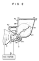
- Developing apparatus 8 comprises housing 30 constituted by back frame 24, bottom frame 26, and front frame 28.
- Housing 30 stores nonmagnetic developer T.
- developing roller 32 for conveying the developer in housing 30 toward photosensitive drum 2 on which a latent image is formed, is interposed between bottom frame 26 and front frame 28.
- Developing roller 32 is arranged adjacent to photosensitive drum 2, and is rotatable in a direction indicated by arrow A in Fig. 2 in synchronism with rotation of drum 2. Therefore, a portion of developing roller 32 is located inside housing 30 to be in contact with developer T, and the other portion on the side of drum 2 is exposed to the outside between bottom frame 26 and front frame 28.
- Developing roller 32 has an aluminum sleeve.
- the outer surface of the sleeve is subjected to sandblasting, and a nickel electroless-plating layer is formed thereon.
- a surface roughness after plating is about l ⁇ m.
- Developer supply roller 34 for supplying developer T to developing roller 32 while charging developer T is arranged adjacent to bottom frame 26 in housing 30. Roller 34 is in rolling contact with roller 32.
- Developer supplying roller 34 is constituted by metal shaft 36, and conductive rubber 38 coated on shaft 36, as shown in Fig. 3.
- a material prepared by mixing carbon or metal powder in neoprene rubber is used.
- conductive urethane can be used in place of the conductive rubber material. Note that shaft 36 is grounded.
- Proximal end portion 44 of elastic blade 42 for forming a thin film layer of developer on developing roller 32 and charging it is mounted on lower end portion 40 of front frame 28 through member 46. Free end portion 48 of elastic blade 42 is urged against developing roller 32 above a contacting point between rollers 34 and 32.
- Stirring blade 50 for stirring the developer inside housing 30 is arranged at substantially the center of housing 30.
- Recovery blade 42 is arranged on bottom frame 26 to abut against developing roller 32.
- Developing bias power source 5l is connected to developing roller 32 and photosensitive drum 2.
- Developer supply roller 34 is rotated in a direction opposite to arrow A at a contacting point with developing roller 32.
- Roller 34 moves toner therearound by a frictional force on its outer peripheral surface, so as to triboelectrically charge the toner particles.
- the toner is charged to be positive (+).
- Roller 34 is grounded, and has a negative (-) charge. Therefore, the toner becomes attached to roller 34 by an electrostatic force, and is moved upon rotation of roller 34. Therefore, since the attached toner particles are moved relatively actively upon rotation of roller 34, they can be sufficiently triboelectrically charged together with the surrounding toner particles.
- the toner particles which become attached to roller 34 and are sufficiently charged are rubbed onto roller 32 at the contacting point between rollers 34 and 32. Upon this rubbing, the toner becomes attached to roller 32.
- the toner attached to roller 32 is urged by blade 42 to be further triboelectrically charged, thus forming a uniform thin layer.
- Roller 32 is rotated in the direction indicated by arrow A and conveys the toner layer to a position facing photosensitive drum 2.
- a bias is applied to roller 32 and drum 2 from power source 5l, so that the toner particles attached to roller 32 fly to drum 2, thus developing a latent image formed thereon.
- the residual toner which is not subjected to development remains on the outer peripheral surface of roller 32. However, the residual toner is further conveyed upon rotation of roller 32, and is recovered in housing 30 via recovery blade 32.
- roller 32 Since roller 32 is urged against roller 34, the residual toner on roller 32 is removed by roller 34.
- the toner removed from roller 32 becomes attached to roller 34, and is triboelectrically charged again.
- the developer supply roller is formed of a conductive material, and triboelectrically charges the toner while electrostatically holding it. Thus, the toner can be reliably and sufficiently charged.
- Figs. 4 and 5 show a modification of developer supply roller 34 used in this embodiment.
- Developer supply roller 52 shown in Fig. 4 has shaft 36 around which metal fiber 54, as a conductive fiber, is wound.
- Metal fiber 54 need only be a conductive fiber, and need not be a metal.
- a conductive fiber prepared by mixing a resin such as rayon, nylon, acrylic resin, or the like with conductive carbon, metal, or the like can be used.
- Developer supply roller 56 shown in Fig. 6 has shaft 36 around which foamed urethane 56 is coated, and endless metallic net 58 is adhered thereon.
- shaft 36 and net 58 can be partially connected to each other.
- the developer supply roller need not always be grounded.
- a voltage can be applied to the roller.
- negatively charged toner is used.
- a plurality of developer supply rollers can be in rolling contact with the developing roller, thus again providing the same effects as above.
- a developer supply member is not limited to a roller but can be an endless conveyor belt.
Landscapes
- Physics & Mathematics (AREA)
- General Physics & Mathematics (AREA)
- Dry Development In Electrophotography (AREA)
- Magnetic Brush Developing In Electrophotography (AREA)
Applications Claiming Priority (2)
| Application Number | Priority Date | Filing Date | Title |
|---|---|---|---|
| JP196606/86 | 1986-08-22 | ||
| JP61196606A JPS6352166A (ja) | 1986-08-22 | 1986-08-22 | 現像装置 |
Publications (1)
| Publication Number | Publication Date |
|---|---|
| EP0257178A1 true EP0257178A1 (en) | 1988-03-02 |
Family
ID=16360549
Family Applications (1)
| Application Number | Title | Priority Date | Filing Date |
|---|---|---|---|
| EP87102206A Withdrawn EP0257178A1 (en) | 1986-08-22 | 1987-02-17 | Developing apparatus |
Country Status (3)
| Country | Link |
|---|---|
| US (1) | US4806992A (ja) |
| EP (1) | EP0257178A1 (ja) |
| JP (1) | JPS6352166A (ja) |
Cited By (5)
| Publication number | Priority date | Publication date | Assignee | Title |
|---|---|---|---|---|
| EP0369774A2 (en) * | 1988-11-15 | 1990-05-23 | Mita Industrial Co., Ltd. | A developing apparatus |
| EP0534671A2 (en) * | 1991-09-27 | 1993-03-31 | Xerox Corporation | Phenolic graphite donor roll |
| FR2691815A1 (fr) * | 1992-06-02 | 1993-12-03 | Seiko Epson Corp | Dispositif de développement pour système électrophotographique. |
| US5878309A (en) * | 1994-10-17 | 1999-03-02 | Canon Kabushiki Kaisha | Toner container, toner container assembling method, process cartridge, and electrophotographic image forming apparatus |
| US6702423B2 (en) | 1998-05-27 | 2004-03-09 | Canon Kabushiki Kaisha | Cleaning device for inkjet printing head, cleaning method for inkjet printing head, inkjet recording apparatus, and wiper |
Families Citing this family (19)
| Publication number | Priority date | Publication date | Assignee | Title |
|---|---|---|---|---|
| JPS63279261A (ja) * | 1987-05-11 | 1988-11-16 | Toshiba Corp | 現像方法 |
| US5084733A (en) * | 1987-10-28 | 1992-01-28 | Canon Kabushiki Kaisha | Developing apparatus having developer layer regulation means |
| JPH02282767A (ja) * | 1989-04-25 | 1990-11-20 | Canon Inc | 現像装置 |
| US5253019A (en) * | 1989-10-30 | 1993-10-12 | Xerox Corporation | Developer material transport |
| US4984019A (en) * | 1990-02-26 | 1991-01-08 | Xerox Corporation | Electrode wire cleaning |
| US5047806A (en) * | 1990-06-14 | 1991-09-10 | Xerox Corporation | Meterless single component development |
| JP2921962B2 (ja) * | 1990-10-31 | 1999-07-19 | 株式会社東芝 | 現像装置 |
| DE4128942C2 (de) * | 1991-01-16 | 1995-06-22 | Ricoh Kk | Entwicklungseinrichtung, welche in einer Bilderzeugungseinrichtung vorgesehen ist |
| JP3126523B2 (ja) * | 1992-11-26 | 2001-01-22 | 株式会社東芝 | 画像形成装置及びプロセスユニット |
| US5666620A (en) * | 1993-12-22 | 1997-09-09 | Canon Kabushiki Kaisha | Developing device for peeling toner using peeling rotary member |
| KR960001929A (ko) * | 1994-06-30 | 1996-01-26 | 김광호 | 전자 사진 현상 장치 |
| US5781830A (en) | 1995-02-17 | 1998-07-14 | Gaylord; Michael F. | Electroless plated magnetic brush roller for xerographic copiers, printers and the like |
| KR0174689B1 (ko) * | 1996-09-11 | 1999-04-01 | 삼성전자주식회사 | 현상롤러의 고스트 방지장치 |
| US6516171B2 (en) * | 1999-05-03 | 2003-02-04 | Hitachi, Ltd. | Color electrographic apparatus with developing device having separated toner supply and recovery chambers |
| US6341420B1 (en) | 2000-08-02 | 2002-01-29 | Static Control Components, Inc. | Method of manufacturing a developer roller |
| KR100503476B1 (ko) * | 2002-08-14 | 2005-07-25 | 삼성전자주식회사 | 레이저 프린터의 토너/현상제 혼합롤러 및 현상장치 |
| US7013104B2 (en) * | 2004-03-12 | 2006-03-14 | Lexmark International, Inc. | Toner regulating system having toner regulating member with metallic coating on flexible substrate |
| US7236729B2 (en) * | 2004-07-27 | 2007-06-26 | Lexmark International, Inc. | Electrophotographic toner regulating member with induced strain outside elastic response region |
| JP2009003029A (ja) * | 2007-06-19 | 2009-01-08 | Seiko Epson Corp | 転造装置、現像ローラの製造方法、現像ローラ、現像装置、および画像形成装置 |
Citations (5)
| Publication number | Priority date | Publication date | Assignee | Title |
|---|---|---|---|---|
| US4083326A (en) * | 1977-02-28 | 1978-04-11 | Eastman Kodak Company | Single component developer applicator apparatus |
| GB2070981A (en) * | 1980-01-18 | 1981-09-16 | Tokyo Shibaura Electric Co | Developing apparatus |
| DE3212865A1 (de) * | 1981-04-07 | 1982-10-14 | Tokyo Shibaura Denki K.K., Kawasaki, Kanagawa | Entwicklungsvorrichtung zur entwicklung eines latenten ladungsbilds |
| GB2163371A (en) * | 1984-08-07 | 1986-02-26 | Ricoh Kk | Developing electrostatic latent images |
| EP0205178A2 (en) * | 1985-06-13 | 1986-12-17 | Matsushita Electric Industrial Co., Ltd. | Developing device |
Family Cites Families (10)
| Publication number | Priority date | Publication date | Assignee | Title |
|---|---|---|---|---|
| US4263391A (en) * | 1978-08-31 | 1981-04-21 | Canon Kabushiki Kaisha | Liquid development process with porous elastic development cleaning roller |
| US4227796A (en) * | 1979-05-29 | 1980-10-14 | Eastman Kodak Company | Electrographic apparatus having improved developer metering construction |
| JPS5640861A (en) * | 1979-09-11 | 1981-04-17 | Canon Inc | Developing device |
| JPS5691261A (en) * | 1979-12-25 | 1981-07-24 | Canon Inc | Developing device |
| JPS59220763A (ja) * | 1983-05-31 | 1984-12-12 | Ricoh Co Ltd | 現像剤担持体の製造方法 |
| JPS60229056A (ja) * | 1984-04-27 | 1985-11-14 | Fuji Xerox Co Ltd | 非磁性一成分現像装置 |
| JPS60229058A (ja) * | 1984-04-27 | 1985-11-14 | Fuji Xerox Co Ltd | 非磁性一成分現像装置 |
| JPS6145255A (ja) * | 1984-08-09 | 1986-03-05 | Ricoh Co Ltd | 現像装置 |
| JPS6152663A (ja) * | 1984-08-22 | 1986-03-15 | Matsushita Electric Ind Co Ltd | 現像装置 |
| JPS61176961A (ja) * | 1985-01-31 | 1986-08-08 | Ricoh Co Ltd | 現像装置 |
-
1986
- 1986-08-22 JP JP61196606A patent/JPS6352166A/ja active Pending
-
1987
- 1987-02-17 EP EP87102206A patent/EP0257178A1/en not_active Withdrawn
- 1987-02-24 US US07/018,208 patent/US4806992A/en not_active Expired - Lifetime
Patent Citations (5)
| Publication number | Priority date | Publication date | Assignee | Title |
|---|---|---|---|---|
| US4083326A (en) * | 1977-02-28 | 1978-04-11 | Eastman Kodak Company | Single component developer applicator apparatus |
| GB2070981A (en) * | 1980-01-18 | 1981-09-16 | Tokyo Shibaura Electric Co | Developing apparatus |
| DE3212865A1 (de) * | 1981-04-07 | 1982-10-14 | Tokyo Shibaura Denki K.K., Kawasaki, Kanagawa | Entwicklungsvorrichtung zur entwicklung eines latenten ladungsbilds |
| GB2163371A (en) * | 1984-08-07 | 1986-02-26 | Ricoh Kk | Developing electrostatic latent images |
| EP0205178A2 (en) * | 1985-06-13 | 1986-12-17 | Matsushita Electric Industrial Co., Ltd. | Developing device |
Non-Patent Citations (3)
| Title |
|---|
| PATENT ABSTRACTS OF JAPAN, vol. 10, no. 212 (P-480)[2268], 24th July 1986; & JP - A - 61 52663 (MATSUSHITA ELECTRIC INDUSTRIAL) 15-03-1986 * |
| PATENT ABSTRACTS OF JAPAN, vol. 5, no. 96 (P-67)[768], 23rd June 1981; & JP - A - 56 40861 (CANON) 17-04-1981 * |
| PATENT ABSTRACTS OF JAPAN, vol. 9, no. 93 (P-351)[1816], 23rd April 1985; & JP - A - 59 220 763 (RICOH) 12-12-1984 * |
Cited By (12)
| Publication number | Priority date | Publication date | Assignee | Title |
|---|---|---|---|---|
| EP0369774A2 (en) * | 1988-11-15 | 1990-05-23 | Mita Industrial Co., Ltd. | A developing apparatus |
| EP0369774A3 (en) * | 1988-11-15 | 1992-04-29 | Mita Industrial Co., Ltd. | A developing apparatus |
| EP0534671A2 (en) * | 1991-09-27 | 1993-03-31 | Xerox Corporation | Phenolic graphite donor roll |
| EP0534671A3 (en) * | 1991-09-27 | 1993-06-09 | Xerox Corporation | Phenolic graphite donor roll |
| FR2691815A1 (fr) * | 1992-06-02 | 1993-12-03 | Seiko Epson Corp | Dispositif de développement pour système électrophotographique. |
| GB2267765A (en) * | 1992-06-02 | 1993-12-15 | Seiko Epson Corp | Developing device |
| US5557060A (en) * | 1992-06-02 | 1996-09-17 | Seiko Epson Corporation | Developing device |
| GB2267765B (en) * | 1992-06-02 | 1996-11-13 | Seiko Epson Corp | Developing device |
| US5655197A (en) * | 1992-06-02 | 1997-08-05 | Seiko Epson Corporation | Developing device |
| US5878309A (en) * | 1994-10-17 | 1999-03-02 | Canon Kabushiki Kaisha | Toner container, toner container assembling method, process cartridge, and electrophotographic image forming apparatus |
| US6215969B1 (en) | 1994-10-17 | 2001-04-10 | Canon Kabushiki Kaisha | Toner container, toner container assembling method, process cartridge, and electrophotographic image forming apparatus |
| US6702423B2 (en) | 1998-05-27 | 2004-03-09 | Canon Kabushiki Kaisha | Cleaning device for inkjet printing head, cleaning method for inkjet printing head, inkjet recording apparatus, and wiper |
Also Published As
| Publication number | Publication date |
|---|---|
| JPS6352166A (ja) | 1988-03-05 |
| US4806992A (en) | 1989-02-21 |
Similar Documents
| Publication | Publication Date | Title |
|---|---|---|
| US4806992A (en) | Developing apparatus | |
| US4745429A (en) | Developing apparatus for an electrostatic photocopier | |
| EP0585882A2 (en) | Developing device and cleaning device used in electrophotographic apparatus | |
| US4566402A (en) | Developing apparatus | |
| US4596455A (en) | Developing apparatus | |
| US3951542A (en) | Developer conveyor device | |
| US4641602A (en) | Developing apparatus | |
| JPS61105573A (ja) | 現像装置 | |
| EP0291296A2 (en) | Method for developing an electrostatic latent image | |
| US4748472A (en) | Developing apparatus with multiple blade developer conditioner | |
| US5016560A (en) | Device for image toner distribution on a developing device | |
| JPS60114891A (ja) | 現像装置 | |
| JPS6257991B2 (ja) | ||
| JPH0244295Y2 (ja) | ||
| US5140373A (en) | Electrostatic latent image developing apparatus with bristle height adjusting member | |
| JPS6114665A (ja) | 現像装置 | |
| JPS6122372A (ja) | 現像装置 | |
| JPH0345238Y2 (ja) | ||
| JP2966024B2 (ja) | 複写機の現像装置 | |
| JP2001051496A (ja) | 現像装置及び画像形成装置 | |
| JPH0641258Y2 (ja) | 現像装置 | |
| JPH01277867A (ja) | 現像装置 | |
| JPH01277869A (ja) | 現像装置 | |
| JPH0744008A (ja) | 現像装置並びに現像方法並びに画像形成装置 | |
| JP3752368B2 (ja) | 画像形成装置 |
Legal Events
| Date | Code | Title | Description |
|---|---|---|---|
| PUAI | Public reference made under article 153(3) epc to a published international application that has entered the european phase |
Free format text: ORIGINAL CODE: 0009012 |
|
| 17P | Request for examination filed |
Effective date: 19870313 |
|
| AK | Designated contracting states |
Kind code of ref document: A1 Designated state(s): DE FR |
|
| 17Q | First examination report despatched |
Effective date: 19900105 |
|
| STAA | Information on the status of an ep patent application or granted ep patent |
Free format text: STATUS: THE APPLICATION IS DEEMED TO BE WITHDRAWN |
|
| 18D | Application deemed to be withdrawn |
Effective date: 19901201 |
|
| RIN1 | Information on inventor provided before grant (corrected) |
Inventor name: YASUDA, SACHIKOC/O PATENT DIVISION Inventor name: ASADA, TOMOYUKIC/O PATENT DIVISION Inventor name: YOSHIDA, MINORUC/O PATENT DIVISION Inventor name: MUKAI, HIDEOC/O PATENT DIVISION |