EP0256267B1 - Mikroprozessor zur Datentransferwiederholung - Google Patents
Mikroprozessor zur Datentransferwiederholung Download PDFInfo
- Publication number
- EP0256267B1 EP0256267B1 EP87109412A EP87109412A EP0256267B1 EP 0256267 B1 EP0256267 B1 EP 0256267B1 EP 87109412 A EP87109412 A EP 87109412A EP 87109412 A EP87109412 A EP 87109412A EP 0256267 B1 EP0256267 B1 EP 0256267B1
- Authority
- EP
- European Patent Office
- Prior art keywords
- signal
- retry
- bus
- microprocessor
- error
- Prior art date
- Legal status (The legal status is an assumption and is not a legal conclusion. Google has not performed a legal analysis and makes no representation as to the accuracy of the status listed.)
- Expired - Lifetime
Links
Images


Classifications
-
- G—PHYSICS
- G06—COMPUTING; CALCULATING OR COUNTING
- G06F—ELECTRIC DIGITAL DATA PROCESSING
- G06F11/00—Error detection; Error correction; Monitoring
- G06F11/07—Responding to the occurrence of a fault, e.g. fault tolerance
- G06F11/14—Error detection or correction of the data by redundancy in operation
- G06F11/1402—Saving, restoring, recovering or retrying
- G06F11/1405—Saving, restoring, recovering or retrying at machine instruction level
- G06F11/141—Saving, restoring, recovering or retrying at machine instruction level for bus or memory accesses
Definitions
- the present invention relates to a microprocessor having an improved method for retrying data transfer cycle.
- a microprocessor of this type is disclosed in U.S. Patent 4,348,722.
- a normal end signal (DTACK) as well as an abnormal end signal (BERR) and a retry request signal (HALT) are used as data transfer response signals in order to retry a data transfer cycle.
- DTACK normal end signal
- BERR abnormal end signal
- HALT retry request signal
- Figs. 1 and 5B of the U.S. Patent 4,348,722 are quoted in Figs. 7 and 8. As shown in Fig. 8, when the data transfer ends abnormally and the retry is requested, the signals BERR and HALT are asserted.
- the retry cannot be requested unless those items have been checked.
- timing of the BERR and HALT signal generation circuit is critical and it is difficult to design an external circuit of the microprocessor.
- the invention is set out in claim 1, It is an object of the present invention to provide a microprocessor which solves the problems encountered in the prior art microprocessor, makes it easy to design an external circuit and improves a retry method of data transfer cycle.
- the number of times of retry of the same data transfer is counted, and if the number of times exceeds a predetermined limit, further retry is inhibited.
- Fig. 1 shows a data processing system in accordance with one embodiment of the present invention.
- Microprocessor 100, memory device 410 and control register device 422 are interconnected through an asynchronous transfer bus 140.
- the asynchronous transfer bus 140 comprises an address line (A) 141, an address strobe line (AS) 142, a read/write command line (R/W) 143, a data line (D) 144, a transfer acknowledge line (DTACK) 145, a fault line (FAULT) 146, a bus error line (BERR) 147 and a special access response line (RMA) 148.
- A address line
- AS address strobe line
- R/W read/write command line
- D data line
- DTACK transfer acknowledge line
- FAULT fault line
- BERR bus error line
- RMA special access response line
- the microprocessor 100 contains a small capacity and high speed cache memory to store input/output data of an arithmetic and logical unit (ALU) contained in the microprocessor 100. High speed data transfer is attainable between the cache memory 401 and the ALU.
- ALU arithmetic and logical unit
- a memory device 410 is provided to assist the data storing function.
- the memory device 410 contains a large capacity and low speed semiconductor memory 412.
- the memory device 410 further contains a magnetic storage device such as a hard disk or floppy disk.
- a control register device 422 is provided between input/output devices (I/O devices) not shown and the asynchronous transfer bus 140. Data entered by input means of the I/O devices is transferred to the microprocessor 100. In other cases, data from the microprocessor 100 is transferred to output means of the I/O devices.
- I/O devices input/output devices
- a parity check circuit 402 connected to the data line of the asynchronous transfer bus 140 checks a parity of the data line 144, and if a parity error is detected, it asserts a bus error signal (BERR) 147.
- BERR bus error signal
- the memory device 410 comprises a memory control circuit 411, a memory circuit 412, an error check circuit 413, an error correction circuit 414 and an address check circuit 415.
- the memory control circuit 411 checks the address line (A) 141 to determine whether it is an access to a memory space or not. If it is the access to the memory space, it checks whether it is the access to a mounted memory space or not, and if it is the access to an unmounted area, it asserts a fault signal (FAULT) 146. If it is the access to the mounted area, it accesses to the memory circuit 412 and asserts a transfer acknowledge signal (DTACK) 145.
- A address line
- DTACK transfer acknowledge signal
- the read data is supplied to the data line D 144 through an output buffer 416 and error is checked by the error check circuit 413. If an error is detected, a bus error signal (BERR) 147 is asserted to request retry of the bus cycle.
- BERR bus error signal
- the address check circuit 415 detects the request of retry of the bus cycle by the ECC (error check and correction) error and the error correction circuit 144 produces an error-corrected data through an output buffer 417.
- the address check circuit 415 asserts the DTACK 145.
- the control register device 420 for the I/O devices comprises a register access circuit 421 and a control register 422.
- the register access circuit checks the address 141 to determine whether it is the access to the control register or not. If it is the access to the control register 422 for the I/O devices, (that is, if the address space is an I/O area), the special access response signal RMA 148 is asserted and the control register is accessed and the DTACK 145 is asserted.
- Fig. 5 shows a relation between the address space and the RMA signal 148.
- the special access response signal RMA 148 is asserted to inhibit retry by a bus error.
- Fig. 2 shows a block diagram which shows a detail of the microprocessor 100.
- the microprocessor 100 comprises a control unit 110, a bus control unit 120 and a bus cycle control circuit 130.
- the control unit 110 When data is transferred, the control unit 110 produces an I/O request signal IOREQ 111.
- a read/write command is issued through a line WRT 112, and in a read-modify-write operation, it is issued through a line RMWC 113.
- the read-modify-write operation means an operation in which data read operation and modify/rewrite operation of the read data are continuously performed.
- the control unit 110 receives a fetch end signal FEND 114 from the bus cycle control circuit 130.
- the fetch end signal is asserted, the bus cycle is terminated and the data transfer to the cache memory 401 of the microprocessor 100 is terminated. If the data transfer ends abnormally, the bus cycle control circuit 130 produces a fetch fault signal FFAULT 115 or fetch bus error signal FBERR 116 instead of the fetch end signal FEND 114.
- the control unit 110 starts a fault exceptional processing routine or bus error exceptional processing routine which will be explained later in detail.
- the bus control unit 120 When the bus control unit 120 receives the I/O request signal 111, it produces an address output enable signal (AEN) 121, an internal signal 122 of the address strobe line 142, an internal signal 123 of the read/write command line 143 and a data output enable signal (DEN) 124 to start the bus cycle. It also produces a signal BCYCECOND 125 to start the bus cycle control circuit 130.
- AEN address output enable signal
- DEN data output enable signal
- the bus cycle control circuit 130 comprises an end detection circuit 131, a retry circuit 132, an end report circuit 133 and a retry counter 134.
- the end detection circuit 131 samples the transfer acknowledge line 145, fault line 146 and bus error line 147, and if one of the signals is asserted, it produces an end of bus cycle signal to report the end of bus cycle to the bus control unit 120.
- the retry circuit 132 responds to the end of bus cycle signal 135 to produce a retry signal RETRY 136 when retry is to be done, or an end signal END 137 when retry is not to be done.
- the retry signal RETRY 136 is supplied to the bus control unit 120 to retry the bus cycle.
- the end signal END 137 is supplied to an end report circuit 133 which generates, together with the fault line 146 and the bus error line 147, the FEND 114, FFAULT 115 and FBERR 116.
- the retry counter 134 is cleared by the IOREQ 111 and counted up by the RETRY 136. When the number of times of retry reaches a predetermined limit, it produces a signal MAXR 138 to inhibit further retry.
- Fig. 3 shows a circuit diagram of the bus cycle control circuit 130.
- the retry circuit 132 asserts the END 137 if the BERR 147 is negated or a signal (NORETRY) 201 to inhibit retry is asserted.
- the retry circuit 132 asserts the RETRY 136.
- the retry inhibit signal (NORETRY) 201 is produced by a logical OR of the special access response signal RMA 148 from the external, the read-modify-write command signal 113 from the control unit 110 and the signal MAXR 138 from the retry counter 134.
- Data transfer errors between the microprocessor 100 and the peripheral equipments (memory device 410, and control register device 420) through the asynchronous transfer bus 140 are classified into several modes.
- the output of the parity check circuit 402 is asserted.
- the output of the error check circuit 413 is asserted.
- the bus error signal BERR applied to the microprocessor 100 is asserted.
- the retry of bidirectional data transfer between the microprocessor 100 and the peripheral equipments 410 and 420 is significant and the retry is performed.
- a bus error is detected in one bus cycle, and in the next bus cycle, the retry is performed and the transfer is terminated.
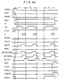
- the bus control unit 120 of the microprocessor 100 starts a first bus cycle T1.
- the address output enable signal AEN 121 is asserted and the address signal A 141, address strobe signal AS 142 and data signal D 144 are supplied from the microprocessor 100 to the asynchronous transfer bus 140. If a slight parity error or soft error is detected in the bus cycle T1, the bus error signal BERR 147 is asserted. Thus, the end of bus cycle signal BCYCEND 135 and the retry signal RETRY 136 are asserted, and the first bus cycle T1 ends and a second bus cycle T2 starts.
- the signal AEN 121 is asserted and the signals A 141, AS 142 and D 144 are supplied from the microprocessor 100 to the bus 140. If the data transfer in the second bus cycle T2 successes (that is, no parity error nor soft error), the transfer acknowledge signal DTACK 145 is asserted, and the end signal END 137 and the fetch end signal FEND 114 is asserted, and the second bus cycle T2 is terminated.
- the retry of data transfer is insignificant for certain access error.
- the microprocessor 100 accesses an unmounted area of the address space of Fig. 5 (that is, an area other than address areas of the memory device 410 and the I/O control register 420), it is insignificant. This may occur when a software programmer uses memory functions in excess of the capacity of the memory device 410.
- the retry of bidirectional data transfer between the microprocessor 100 and the peripheral equipments 410 and 420 is insignificant and the retry is not performed.
- Fig. 4b a fault is detected in one bus cycle and retry is not performed in the next bus cycle.
- the memory control circuit 411 of the memory device 410 When the address signal A 141 accesses an unmounted area of the address space of Fig. 5, the memory control circuit 411 of the memory device 410 asserts the fault signal FAULT 146, which is supplied to the bus cycle control circuit 130 of the microprocessor 100 through the asynchronous transfer bus 140. In this case, since the retry signal RETRY 136 is not asserted by the memory control circuit 130 in the bus cycle T1, the bus control unit 120 does not perform the retry. On the other hand, the bus cycle control circuit 130 asserts the end of bus cycle signal BCYCEND 135, end signal END 137 and fetch fault signal FFAULT 114.
- the control unit 110 of the microprocessor 100 commands the fault exceptional processing routine, which informs the fact that the address signal has accessed the unmounted area, to programmer, operator and user through the output means of the I/O devices.
- the address signal A 141 accesses the I/O area of the address space of Fig. 5.
- the bus error signal BERR 147 is asserted when the address signal A 141 accesses the input means of the I/O equipments, it means that there is a data error such as a parity error in the data signal D 144 transferred from the input means of the I/O equipments to the microprocessor 100 through the asynchronous transfer bus.
- the bus error signal BERR 147 is asserted and the retry of data transfer from the input means to the microprocessor 100 is insignificant.
- Fig. 4c shows that retry of data transfer is not performed in such case.
- the register access circuit 421 of the control register device 420 asserts the special access response signal RMA 148.
- the bus error signal BERR 147 is asserted by the data error in the data signal D 144, as described above.
- the asserted signal RMA 148 is supplied to the bus cycle control circuit 130 of the microprocessor 100 through the asynchronous transfer bus 140. In this case, since the retry signal RETRY 136 is not asserted by the memory control circuit 130 in the bus cycle T1, the bus control unit 120 does not retry the data transfer.
- the bus cycle control circuit 130 asserts the end of bus cycle signal BCYCEND 135, end signal END 137 and fetch bus error signal FBERR 116.
- the control unit 110 of the microprocessor 100 commands the bus error exceptional processing routine, which checks status of the input means of the I/O devices and informs to a user through the output means of the I/O equipments that the input job by the input means should be retried.
- a serious parity error or soft error may take place for a long period of time in the data signal D 144 by the soft error of the memory circuit of the memory device 410 due to electromagnetic interference around the microprocessor or abnormal increase of irradiated ⁇ particles.
- the data transfer is not successful even if the retry shown in Fig. 4a is repeated. If the retry of data transfer is endlessly repeated, the microprocessor 100 endlessly repeats useless routine and a significant time is required for the user to recognize such abnormal state.
- a limit is set to the number of times of repetition of retry, and if the retry does not success before the limit is reached, the bus error exceptional processing routine is executed to inform the abnormal state to the user and further retry is inhibited.
- Fig. 4c illustrates this operation.
- the bus error signal BERR 147 is asserted in the (n-1)th bus cycle T n-1 but the transfer acknowledge signal DTACK 145 is not asserted.
- the (n-2)th retry signal RETRY 136 is applied to the retry counter 134 of the bus cycle control circuit 130 of Fig. 3, the signal MAXR 138 is asserted by the circuit 130.
- the retry signal RETRY 136 is no longer asserted while the end of bus cycle signal BCYCEND 135, end signal END 137 and fetch bus error signal FBERR 116 are asserted.
- the control unit 110 of the microprocessor 100 executes the bus error exceptional processing routine to inform the abnormal state.
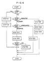
- Fig. 6 shows a flow chart of the operation of the data processing system shown in Fig. 1.
- step 510 When the data transfer is started, the address is first checked, and if it is a retry cycle by an ECC error (step 510), a corrected data is sent (step 511) and the DTACK 145 is asserted (step 512).
- the flow of the steps 510 - 512 corresponds to the retry of Fig. 4a.
- step 520 whether the access space is a memory area or a register area is checked (step 520), and if it is the register area, the RMA 148 is asserted (step 521), the register is accessed (step 522) and the DTACK 145 is asserted (step 523).
- the flow of the steps 520 - 523 corresponds to the non-retry operation of Fig. 4c.
- the access space is the memory area, whether it is a mounted area or not is checked (step 530), and if it is unmounted, the FAULT 146 is asserted (step 531). If it is mounted, the memory is accessed (step 540), the DTACK 145 is asserted (step 550) and the ECC check is performed (step 560). If an ECC error is detected, the BERR 147 is asserted (step 561). On the other hand, the flow of the steps 530 - 531 corresponds to the non-retry operation of Fig. 4b.
- the ECC check of the memory device and the correction are divided into two bus cycles. In the first cycle, the memory readout and the ECC check are performed, and in the second bus cycle, the correction and the data transfer are performed. Accordingly, high speed memory access is attained when ECC error is not included.
- the retry of the bus cycle is started by one external input signal. Accordingly, a timing margin of the retry start circuit is large and high speed data transfer is attained. Further, it is possible to have an external input signal for inhibiting retry. In this case, a malfunction due to the retry access to the control register can be prevented.
- the retry may be inhibited by the command of the control unit in the processor. Accordingly, the retry may be inhibited in the read-modify-write cycle to prevent malfunction. The number of times of retry is counted and if a bus error is still detected when the number of times reaches the limit, the retry is inhibited. Accordingly, an endless loop of retry is prevented and a reliability of the system is improved.
- the data processing system which transfers data to and from the external equipment, if the data transfer ends abnormally, the retry of the data transfer is requested by the signal from the input means. Accordingly, the design of the external circuit is facilitated and the data processing system which performs the retry of the data transfer cycle in a manner suitable to the microprocessor is provided.
Claims (4)
- Mikroprozessor zum Austauschen von Daten mit einem Peripheriegerät über einen Bus (140) mit:(a) einer Bussteuereinheit (120) zum Eingeben wenigstens eines Adreßsignals und eines Datensignals in den Bus (140), und(b) einer mit dem Bus (140) und der Bussteuereinheit (120) verbundenen Steuervorrichtung (110, 130), die eine erste Einrichtung (132) aufweist, die auf ein erstes Signal (BERR 147) von dem Peripheriegerät anspricht, das anzeigt, daß ein Fehler während der Datenübertragung über den Bus (140) aufgetreten ist, wobei die erste Einrichtung (132) bewirkt, daß ein zweites Signal (RETRY 136) erzeugt wird, das die Bussteuereinheit (120) anweist, die Datenübertragung zu wiederholen,dadurch gekennzeichnet,
daß die Steuervorrichtung (110, 130) weiter eine zweite Einrichtung (131) aufweist, die ansprechend auf ein drittes Signal (FAULT 146) von dem Peripheriegerät, das anzeigt, daß das Adreßsignal einem Zugriff auf einen nicht vorhandenen Bereich in einem Adreßraum des Mikroprozessors entspricht, ein Ausgangssignal (NORETRY 201) erzeugt, das das Wiederholen blockiert. - Mikroprozessor nach Anspruch 1, wobei die Steuervorrichtung (110, 130) weiter eine dritte Einrichtung (133) aufweist, die ansprechend auf das von der zweiten Einrichtung (131) gelieferte Wiederholungssperrsignal (NORETRY 201) den Benutzer über eine Ausgabeeinrichtung eines E/A-Geräts des Peripheriegeräts davon unterrichtet, daß das Adreßsignal einem Zugriff auf einen nicht vorhandenen Bereich entspricht.
- Mikroprozessor nach Anspruch 1, wobei das erste Signal (BERR 147) anzeigt, daß der Fehler während des Datenaustausches mit einem vorhandenen Speicherbereich in dem Adreßraum des Peripheriegeräts aufgetreten ist.
- Mikroprozessor nach Anspuch 3, wobei die Steuervorrichtung (110, 130) weiter eine vierte Einrichtung (134) aufweist, die die Anzahl der v on der ersten Einrichtung (132) angeordneten Wiederholungen zählt und ein weiteres Wiederholen blockiert, wenn die Zahl einen vorbestimmten Wert erreicht.
Priority Applications (1)
| Application Number | Priority Date | Filing Date | Title |
|---|---|---|---|
| EP92106804A EP0498472B1 (de) | 1986-08-12 | 1987-06-30 | Mikroprozessor zur Datentransferwiederholung |
Applications Claiming Priority (2)
| Application Number | Priority Date | Filing Date | Title |
|---|---|---|---|
| JP189201/86 | 1986-08-12 | ||
| JP18920186 | 1986-08-12 |
Related Child Applications (1)
| Application Number | Title | Priority Date | Filing Date |
|---|---|---|---|
| EP92106804.5 Division-Into | 1992-04-21 |
Publications (3)
| Publication Number | Publication Date |
|---|---|
| EP0256267A2 EP0256267A2 (de) | 1988-02-24 |
| EP0256267A3 EP0256267A3 (en) | 1989-10-25 |
| EP0256267B1 true EP0256267B1 (de) | 1994-03-02 |
Family
ID=16237213
Family Applications (2)
| Application Number | Title | Priority Date | Filing Date |
|---|---|---|---|
| EP87109412A Expired - Lifetime EP0256267B1 (de) | 1986-08-12 | 1987-06-30 | Mikroprozessor zur Datentransferwiederholung |
| EP92106804A Expired - Lifetime EP0498472B1 (de) | 1986-08-12 | 1987-06-30 | Mikroprozessor zur Datentransferwiederholung |
Family Applications After (1)
| Application Number | Title | Priority Date | Filing Date |
|---|---|---|---|
| EP92106804A Expired - Lifetime EP0498472B1 (de) | 1986-08-12 | 1987-06-30 | Mikroprozessor zur Datentransferwiederholung |
Country Status (5)
| Country | Link |
|---|---|
| US (1) | US4845614A (de) |
| EP (2) | EP0256267B1 (de) |
| JP (1) | JP2708427B2 (de) |
| KR (1) | KR950001420B1 (de) |
| DE (2) | DE3789176T2 (de) |
Families Citing this family (27)
| Publication number | Priority date | Publication date | Assignee | Title |
|---|---|---|---|---|
| JP2593339B2 (ja) * | 1988-06-10 | 1997-03-26 | 富士写真フイルム株式会社 | マイクロフィルム検索・読取装置 |
| US5018063A (en) * | 1988-12-05 | 1991-05-21 | International Business Machines Corporation | Method for reducing cross-interrogate delays in a multiprocessor system |
| JPH07120292B2 (ja) * | 1989-06-19 | 1995-12-20 | 日本電気株式会社 | 情報処理システム |
| US5153881A (en) * | 1989-08-01 | 1992-10-06 | Digital Equipment Corporation | Method of handling errors in software |
| US5220651A (en) * | 1989-10-11 | 1993-06-15 | Micral, Inc. | Cpu-bus controller for accomplishing transfer operations between a controller and devices coupled to an input/output bus |
| DE69231720T2 (de) * | 1991-12-10 | 2001-06-21 | Fujitsu Ltd | Speicherzugriffsvorrichtung mit Adresspipeline |
| US5500950A (en) * | 1993-01-29 | 1996-03-19 | Motorola, Inc. | Data processor with speculative data transfer and address-free retry |
| EP0764907A1 (de) | 1995-09-22 | 1997-03-26 | International Business Machines Corporation | Verfahren und System zur Fehlerkorrektur in einem Datenverarbeitungssystem |
| US5566348A (en) * | 1995-10-22 | 1996-10-15 | International Business Machines Corporation | System for adaptively optimizing automated optical library management |
| JP2000148604A (ja) | 1998-11-12 | 2000-05-30 | Hitachi Ltd | 記憶装置の制御方法 |
| KR20000045794A (ko) * | 1998-12-30 | 2000-07-25 | 서평원 | 스카시 버스 장애시의 재접속 방법 |
| US6687846B1 (en) * | 2000-03-30 | 2004-02-03 | Intel Corporation | System and method for error handling and recovery |
| US7020709B1 (en) | 2000-06-30 | 2006-03-28 | Intel Corporation | System and method for fault tolerant stream splitting |
| US7318107B1 (en) | 2000-06-30 | 2008-01-08 | Intel Corporation | System and method for automatic stream fail-over |
| AUPQ866000A0 (en) * | 2000-07-07 | 2000-08-03 | Activesky, Inc. | A secure data storage device |
| US7093154B2 (en) * | 2001-10-25 | 2006-08-15 | International Business Machines Corporation | Critical adapter local error handling |
| US20060047855A1 (en) | 2004-05-13 | 2006-03-02 | Microsoft Corporation | Efficient chunking algorithm |
| US7487395B2 (en) * | 2004-09-09 | 2009-02-03 | Microsoft Corporation | Method, system, and apparatus for creating an architectural model for generating robust and easy to manage data protection applications in a data protection system |
| US7865470B2 (en) * | 2004-09-09 | 2011-01-04 | Microsoft Corporation | Method, system, and apparatus for translating logical information representative of physical data in a data protection system |
| US7567974B2 (en) | 2004-09-09 | 2009-07-28 | Microsoft Corporation | Method, system, and apparatus for configuring a data protection system |
| US8145601B2 (en) | 2004-09-09 | 2012-03-27 | Microsoft Corporation | Method, system, and apparatus for providing resilient data transfer in a data protection system |
| US7613787B2 (en) | 2004-09-24 | 2009-11-03 | Microsoft Corporation | Efficient algorithm for finding candidate objects for remote differential compression |
| US20060218435A1 (en) * | 2005-03-24 | 2006-09-28 | Microsoft Corporation | Method and system for a consumer oriented backup |
| JP2007018454A (ja) * | 2005-07-11 | 2007-01-25 | Toshiba Corp | マイクロプロセッサ |
| US7529866B2 (en) | 2005-11-17 | 2009-05-05 | P.A. Semi, Inc. | Retry mechanism in cache coherent communication among agents |
| US7571266B2 (en) * | 2006-02-06 | 2009-08-04 | Carlson Lance R | Peripheral device in a computerized system and method |
| US7752340B1 (en) * | 2006-03-31 | 2010-07-06 | Emc Corporation | Atomic command retry in a data storage system |
Family Cites Families (8)
| Publication number | Priority date | Publication date | Assignee | Title |
|---|---|---|---|---|
| US3539996A (en) * | 1968-01-15 | 1970-11-10 | Ibm | Data processing machine function indicator |
| GB1315673A (en) * | 1970-06-12 | 1973-05-02 | Robotron Veb K | Digital computer installations |
| US4017840A (en) * | 1973-06-15 | 1977-04-12 | Gte Automatic Electric Laboratories Incorporated | Method and apparatus for protecting memory storage location accesses |
| US4348722A (en) * | 1980-04-03 | 1982-09-07 | Motorola, Inc. | Bus error recognition for microprogrammed data processor |
| US4417334A (en) * | 1981-04-16 | 1983-11-22 | Ncr Corporation | Data processing system having dual-channel system bus |
| US4524415A (en) * | 1982-12-07 | 1985-06-18 | Motorola, Inc. | Virtual machine data processor |
| US4621323A (en) * | 1983-03-28 | 1986-11-04 | Digital Equipment Corporation | Message transmission circuitry |
| US4616335A (en) * | 1983-06-30 | 1986-10-07 | International Business Machines Corporation | Apparatus for suspending a system clock when an initial error occurs |
-
1987
- 1987-06-30 DE DE3789176T patent/DE3789176T2/de not_active Expired - Fee Related
- 1987-06-30 EP EP87109412A patent/EP0256267B1/de not_active Expired - Lifetime
- 1987-06-30 DE DE3750662T patent/DE3750662T2/de not_active Expired - Fee Related
- 1987-06-30 EP EP92106804A patent/EP0498472B1/de not_active Expired - Lifetime
- 1987-07-23 KR KR1019870008012A patent/KR950001420B1/ko not_active IP Right Cessation
- 1987-07-31 JP JP62190013A patent/JP2708427B2/ja not_active Expired - Fee Related
- 1987-08-10 US US07/083,169 patent/US4845614A/en not_active Expired - Lifetime
Also Published As
| Publication number | Publication date |
|---|---|
| EP0256267A2 (de) | 1988-02-24 |
| US4845614A (en) | 1989-07-04 |
| KR880003244A (ko) | 1988-05-14 |
| KR950001420B1 (ko) | 1995-02-24 |
| DE3750662D1 (de) | 1994-11-17 |
| EP0498472A2 (de) | 1992-08-12 |
| DE3750662T2 (de) | 1995-02-16 |
| EP0498472A3 (en) | 1992-11-04 |
| EP0498472B1 (de) | 1994-10-12 |
| JP2708427B2 (ja) | 1998-02-04 |
| EP0256267A3 (en) | 1989-10-25 |
| JPS63153657A (ja) | 1988-06-27 |
| DE3789176D1 (de) | 1994-04-07 |
| DE3789176T2 (de) | 1994-09-08 |
Similar Documents
| Publication | Publication Date | Title |
|---|---|---|
| EP0256267B1 (de) | Mikroprozessor zur Datentransferwiederholung | |
| FI92262C (fi) | Joustava väyläjärjestelmä | |
| EP0479230B1 (de) | Wiederherstellungsverfahren und Gerät für eine Pipeline-Verarbeitungseinheit eines Multiprozessor-systems | |
| CA1323441C (en) | Fault tolerant digital data processor with improved input/output controller | |
| US4740969A (en) | Method and apparatus for recovering from hardware faults | |
| US3800294A (en) | System for improving the reliability of systems using dirty memories | |
| EP0676696B1 (de) | Parallelschlussschnittstellenschaltkreise in Rechnersystemen | |
| JPH02202638A (ja) | 多重プロセッサを備えたフォールトトレラントなコンピュータシステム | |
| US5293384A (en) | Microprocessor bus interface protocol analyzer | |
| EP0529557B1 (de) | Gerät zur Vermeidung der Zerstörung von aus Speichereinheit gelesenen Rechnerdaten | |
| JPH0750452B2 (ja) | バストレース機構 | |
| JP3311776B2 (ja) | ディスクサブシステムにおけるデータ転送チェック方式 | |
| JP3190694B2 (ja) | ローカルメモリの診断方式 | |
| JP2584466B2 (ja) | ディスクコントローラの自己診断方法 | |
| JPS639259B2 (de) | ||
| JPS5987658A (ja) | 故障デ−タ転送装置 | |
| JPS6158033A (ja) | デイスク制御装置 | |
| JPH03230216A (ja) | 記憶デバイスへの処理データの書込処理方式 | |
| JPS6041383B2 (ja) | 共通バス監視方式 | |
| JPH05324487A (ja) | メモリ制御システム | |
| JPS5829062A (ja) | マイクロコンピユ−タシステム | |
| JPH0423294B2 (de) | ||
| JPS6156537B2 (de) | ||
| JPH02230340A (ja) | エラー情報ロギングシステム | |
| JPH083803B2 (ja) | Nmi処理方法 |
Legal Events
| Date | Code | Title | Description |
|---|---|---|---|
| PUAI | Public reference made under article 153(3) epc to a published international application that has entered the european phase |
Free format text: ORIGINAL CODE: 0009012 |
|
| AK | Designated contracting states |
Kind code of ref document: A2 Designated state(s): DE FR GB IT |
|
| PUAL | Search report despatched |
Free format text: ORIGINAL CODE: 0009013 |
|
| AK | Designated contracting states |
Kind code of ref document: A3 Designated state(s): DE FR GB IT |
|
| 17P | Request for examination filed |
Effective date: 19900329 |
|
| 17Q | First examination report despatched |
Effective date: 19911211 |
|
| GRAA | (expected) grant |
Free format text: ORIGINAL CODE: 0009210 |
|
| AK | Designated contracting states |
Kind code of ref document: B1 Designated state(s): DE FR GB IT |
|
| REF | Corresponds to: |
Ref document number: 3789176 Country of ref document: DE Date of ref document: 19940407 |
|
| ITF | It: translation for a ep patent filed |
Owner name: MODIANO & ASSOCIATI S.R.L. |
|
| ET | Fr: translation filed | ||
| PLBE | No opposition filed within time limit |
Free format text: ORIGINAL CODE: 0009261 |
|
| STAA | Information on the status of an ep patent application or granted ep patent |
Free format text: STATUS: NO OPPOSITION FILED WITHIN TIME LIMIT |
|
| 26N | No opposition filed | ||
| PGFP | Annual fee paid to national office [announced via postgrant information from national office to epo] |
Ref country code: GB Payment date: 19990330 Year of fee payment: 13 |
|
| PGFP | Annual fee paid to national office [announced via postgrant information from national office to epo] |
Ref country code: FR Payment date: 19990419 Year of fee payment: 13 |
|
| PGFP | Annual fee paid to national office [announced via postgrant information from national office to epo] |
Ref country code: DE Payment date: 19990824 Year of fee payment: 13 |
|
| PG25 | Lapsed in a contracting state [announced via postgrant information from national office to epo] |
Ref country code: GB Free format text: LAPSE BECAUSE OF NON-PAYMENT OF DUE FEES Effective date: 20000630 |
|
| GBPC | Gb: european patent ceased through non-payment of renewal fee |
Effective date: 20000630 |
|
| PG25 | Lapsed in a contracting state [announced via postgrant information from national office to epo] |
Ref country code: FR Free format text: LAPSE BECAUSE OF NON-PAYMENT OF DUE FEES Effective date: 20010228 |
|
| REG | Reference to a national code |
Ref country code: FR Ref legal event code: ST |
|
| PG25 | Lapsed in a contracting state [announced via postgrant information from national office to epo] |
Ref country code: DE Free format text: LAPSE BECAUSE OF NON-PAYMENT OF DUE FEES Effective date: 20010403 |
|
| PG25 | Lapsed in a contracting state [announced via postgrant information from national office to epo] |
Ref country code: IT Free format text: LAPSE BECAUSE OF NON-PAYMENT OF DUE FEES;WARNING: LAPSES OF ITALIAN PATENTS WITH EFFECTIVE DATE BEFORE 2007 MAY HAVE OCCURRED AT ANY TIME BEFORE 2007. THE CORRECT EFFECTIVE DATE MAY BE DIFFERENT FROM THE ONE RECORDED. Effective date: 20050630 |