EP0254871A2 - Umgekehrtes Dunkelfeld-Ausrichtsystem für einen lithographischen Ausrichtscanner - Google Patents
Umgekehrtes Dunkelfeld-Ausrichtsystem für einen lithographischen Ausrichtscanner Download PDFInfo
- Publication number
- EP0254871A2 EP0254871A2 EP87109074A EP87109074A EP0254871A2 EP 0254871 A2 EP0254871 A2 EP 0254871A2 EP 87109074 A EP87109074 A EP 87109074A EP 87109074 A EP87109074 A EP 87109074A EP 0254871 A2 EP0254871 A2 EP 0254871A2
- Authority
- EP
- European Patent Office
- Prior art keywords
- wafer
- alignment
- reticle
- target
- light
- Prior art date
- Legal status (The legal status is an assumption and is not a legal conclusion. Google has not performed a legal analysis and makes no representation as to the accuracy of the status listed.)
- Granted
Links
- 238000005286 illumination Methods 0.000 claims description 17
- 238000000034 method Methods 0.000 claims description 11
- 238000003384 imaging method Methods 0.000 claims description 2
- 239000000758 substrate Substances 0.000 description 15
- 238000000576 coating method Methods 0.000 description 13
- 239000011248 coating agent Substances 0.000 description 11
- 230000003287 optical effect Effects 0.000 description 7
- 238000001514 detection method Methods 0.000 description 6
- 230000008569 process Effects 0.000 description 6
- 230000005855 radiation Effects 0.000 description 6
- 230000033001 locomotion Effects 0.000 description 5
- 229920002120 photoresistant polymer Polymers 0.000 description 5
- 238000012937 correction Methods 0.000 description 3
- 238000000926 separation method Methods 0.000 description 3
- 238000010586 diagram Methods 0.000 description 2
- 230000006872 improvement Effects 0.000 description 2
- 238000005259 measurement Methods 0.000 description 2
- 238000000206 photolithography Methods 0.000 description 2
- 239000004065 semiconductor Substances 0.000 description 2
- 238000006424 Flood reaction Methods 0.000 description 1
- 238000013459 approach Methods 0.000 description 1
- 230000002238 attenuated effect Effects 0.000 description 1
- 230000008859 change Effects 0.000 description 1
- 238000010276 construction Methods 0.000 description 1
- 230000001186 cumulative effect Effects 0.000 description 1
- 230000001419 dependent effect Effects 0.000 description 1
- 238000000151 deposition Methods 0.000 description 1
- 238000011161 development Methods 0.000 description 1
- 239000002019 doping agent Substances 0.000 description 1
- 230000000694 effects Effects 0.000 description 1
- 230000008570 general process Effects 0.000 description 1
- 239000012535 impurity Substances 0.000 description 1
- 230000007246 mechanism Effects 0.000 description 1
- 238000012986 modification Methods 0.000 description 1
- 230000004048 modification Effects 0.000 description 1
- 238000012545 processing Methods 0.000 description 1
- 230000001681 protective effect Effects 0.000 description 1
- 238000002310 reflectometry Methods 0.000 description 1
- 230000004044 response Effects 0.000 description 1
- 239000007787 solid Substances 0.000 description 1
- 230000003746 surface roughness Effects 0.000 description 1
- 238000012876 topography Methods 0.000 description 1
- 238000011179 visual inspection Methods 0.000 description 1
Images

Classifications
-
- G—PHYSICS
- G03—PHOTOGRAPHY; CINEMATOGRAPHY; ANALOGOUS TECHNIQUES USING WAVES OTHER THAN OPTICAL WAVES; ELECTROGRAPHY; HOLOGRAPHY
- G03F—PHOTOMECHANICAL PRODUCTION OF TEXTURED OR PATTERNED SURFACES, e.g. FOR PRINTING, FOR PROCESSING OF SEMICONDUCTOR DEVICES; MATERIALS THEREFOR; ORIGINALS THEREFOR; APPARATUS SPECIALLY ADAPTED THEREFOR
- G03F7/00—Photomechanical, e.g. photolithographic, production of textured or patterned surfaces, e.g. printing surfaces; Materials therefor, e.g. comprising photoresists; Apparatus specially adapted therefor
- G03F7/20—Exposure; Apparatus therefor
-
- G—PHYSICS
- G03—PHOTOGRAPHY; CINEMATOGRAPHY; ANALOGOUS TECHNIQUES USING WAVES OTHER THAN OPTICAL WAVES; ELECTROGRAPHY; HOLOGRAPHY
- G03F—PHOTOMECHANICAL PRODUCTION OF TEXTURED OR PATTERNED SURFACES, e.g. FOR PRINTING, FOR PROCESSING OF SEMICONDUCTOR DEVICES; MATERIALS THEREFOR; ORIGINALS THEREFOR; APPARATUS SPECIALLY ADAPTED THEREFOR
- G03F9/00—Registration or positioning of originals, masks, frames, photographic sheets or textured or patterned surfaces, e.g. automatically
- G03F9/70—Registration or positioning of originals, masks, frames, photographic sheets or textured or patterned surfaces, e.g. automatically for microlithography
- G03F9/7069—Alignment mark illumination, e.g. darkfield, dual focus
Definitions
- the present invention relates to photolithography systems in general and, more particularly, to such systems wherein reticle-to-wafer alignment is achieved automatically.
- the general process followed is that of generating an oxide film on the semiconductor substrate; coating the oxide film with a photoresist and then exposing the photoresist, through a mask, to radiation.
- the mask has a pattern of opaque or transparent portions thereon. After exposure, the photoresist is developed creating a pattern of exposed or unexposed portions corresponding to the pattern of transparent or opaque portions of the mask.
- the photoresist that remains after developing forms a protective cover for the oxide layer.
- the exposed portion of the oxide layer is then etched to expose portions of the substrate layer below it. Impurities can then be doped into the substrate to give it electrical properties characteristic of the particular dopant/substrate combination created. Once done, the process may be repeated a number of times with additional oxide films formed, more resist deposited, the resist exposed, developed, and the oxide film etched with further steps of doping or depositing carried out.
- a promising approach to automatic wafer-to-reticle alignment is offered by the dark-field alignment concept. It was recognized early in the development of automatic wafer-to-reticle alignment systems that the only reliable system capable of working with complex topographies, covered with photoresist, had to be based on dark field imaging.
- This concept generally, calls for alignment marks, or wafer targets, on the wafer to be illuminated by an alignment illumination source. Light from the alignment illumination source typically floods the wafer surface and is backscattered by edges of the wafer target and reflected by the wafer target itself. The intensity and position of backscattered radiation is detected and compared with the position of alignment features on the reticle to determine the degree of alignment or misalignment between the mask and reticle.
- the reverse dark-field system is an improvement over such prior art dark-field systems.
- the improvement of the reverse dark-field alignment system over the prior art dark-field system is expected because the method has inherently lower background light levels, is less dependent on the quality of the light collection optics, and because symmetrical illumination can easily be achieved.
- a reverse dark-field system is also less susceptible to process induced variations of target profiles.
- the invention provides, in one form thereof, a new and improved alignment system for automatic mask-to-reticle alignment in a scanning exposure system.
- a target including two quadrilateral areas, is formed by known photolithographic processes on a wafer along with a circuit layer.
- An image of a slit mask is projected onto the wafer.
- the slit image has two orthogonal slits oriented in the same direction as the target.
- the wafer, hence the target scans past the slit image.
- the edges of the target back-scatter radiation which is subsequently passed through a field stop and aperture stop, to pass only desired radiation, and then detected.
- the slit images are made longer than the target bars so that light from a portion of the slit image is specularly reflected by the wafer.
- the reticle or mask scans through this reflected slit image and the light passes through reticle targets, which are narrow transmitting windows, and modulate the transmitted light as the reticle scans past the reflected slit image.
- the light which passes through the reticle target is then detected.
- the positions of both the wafer and the reticle are known relative to the slit image. In this way information on the relative positions of the reticle and wafer and magnification can be extracted.
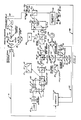
- Fig. l is a schematic diagram showing an alignment system.
- a multi-wavelength laser l0 which is the source of alignment illumination, emits a small collimated beam of light which is enlarged in diameter by a beam expander l2.
- a beamsplitter l4 divides the beam into a first beam ll and a second beam l3.
- a first cylindrical lens l6 is disposed in the path of the first beam ll to focus the first beam ll to a line focus.
- the first beam, emanating from cylindrical lens l6, is redirected by a mirror 20 to a fieldsplitter 24 where it comes to a focus on a slit mask 22.
- the location and function of the slit mask is explained below.
- the second beam l3 is redirected by a mirror l5 to a second cylindrical lens l8 which brings the second beam l3 to a line focus on slit mask 22 in the fieldsplitter 24.
- the slit mask 22 is planar and has two slits 2l and 23 which are at right angles to each other and slightly displaced to avoid overlap.
- the slit mask 22 is so located and the fieldsplitter 24 so constructed that the line foci from cylindrical lenses l6 and l8 coincide with the slits 2l and 23, respectively.
- This illuminated slit mask 22 is in the object plane of an optical relay, shown in Fig. l as a pair of lenses 30 and 34, which forms an image at plane 62.
- a beamsplitter 26 directs a portion of the light passing through slit mask 22 to a lower scan arm, not shown, via path 28.
- the purpose and operation of the lower scan arm will be explained hereinbelow.
- the aperture stop/mirror 32 comprises a substrate 29, which is transparent to the light from laser l0, upon one side of which is disposed an annular opaque coating 3l and an annular reflective coating 33 on the other side. It should be noted that coatings 3l and 33 can be combined into one coating provided that such coating performs the functions hereindescribed and attributed to both coatings 3l and 33.
- the substrate 29 is disposed at an angle, e.g., 45° with respect to the optical axis 35 of the light passing through the substrate 29.
- the annular reflective coating 33 and annular opaque coating are of an elliptical shape.
- the aperture stop/mirror 32 limits the numerical aperture of the relay, which consists of lenses 30 and 34, to a value less than that necessary to fill the numerical aperture of the projection optics 84.
- the numerical aperture of the relay, lenses 30 and 34 can be, for example, 70% of the NA of the projection optics 84.
- the image in the image plane 62 of the relay lenses 30 and 34 is relayed to another image plane 78 by an optical system or relay consisting of lenses 70 and 76 and mirrors 72 and 74.
- the optical system of lenses 70 and 76 can be rotated about optical axis 35 so that the image plane 78 can be placed at any of a number of locations along an arc. This accommodates variable alignment target locations (sub-field heights).
- the image at image plane 78 is redirected by a beamsplitter 80 and is relayed by projection optics 84 to the wafer 86.
- the reticle 82 and wafer 86 move relative to the projection optics 84 during a scanning operation. This provides the exposure of a portion of the wafer 86 under reticle 82 by illumination light 90 which is condensed by a condenser relay 88 and passes through the reticle 82.
- illumination light 90 which is condensed by a condenser relay 88 and passes through the reticle 82.
- the mechanism and procedure is not part of the present invention and will not be discussed further.
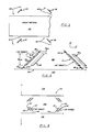
- Fig. 2 is a plan view of a section of the wafer 86.
- a plurality of subfields or circuit patterns such as l04, which are the first layer of a circuit being built of many layers.
- Adjoining the circuit patterns l04 are scribe alleys l06, l08.
- scribe alley l08 is a row of identical alignment targets ll0 which have been established along with the first layer of the circuit patterns l04 through the photolithographic techniques previously described.
- the reticle 82 under which the wafer 86 is exposed to produce the alignment targets ll0 is shown in Fig. 4 and described in reference thereto.
- Fig. 3 shows an enlarged plan view of one of the targets ll0 of Fig. 2.
- the wafer targets lll and ll2 are a pair of quadrilateral areas, e.g. ll6 ⁇ m long, that are, for example, about 7 ⁇ m wide and oriented at ⁇ 45° to the scan direction, as shown by an arrow ll8. These dimensions, and those shown in Fig. 3 are for the purposes of example only.
- the wafer targets lll and ll2 extend above or below the surface of the scribe alley l08 a small distance.
- the wafer targets lll and ll2 are made long to reduce noise effects due to low scattered light levels and due to surface roughness of the wafer 86.
- the alignment image projected onto the wafer in the manner described hereinabove, comprises two bars of light ll4 and ll5.
- the two bars of light ll4 and ll5 can be, for example, l ⁇ m wide.
- the wafer targets lll and ll2 are made wide compared to the width, of the bars of light ll4 and ll5, respectively, projected on them. This ensures that the signal peaks generated by each target edge as the wafer target scans across the slit image are distinct. If the wafer target is too narrow, the peaks can overlap and make processing of the signal difficult and susceptible to errors from unequal peak heights.
- a portion of the beam is transmitted through the beamsplitter 64 to the aperture stop/mirror 32.
- the central portion of the substrate 29 transmits about 90% and reflects l0% of the light incident thereon. Thus, most of the light that was specularly reflected by the wafer passes through the central portion of the aperture stop/mirror 32.
- the scattered light is reflected at 45° incidence by the reflecting coating 33 on the substrate. In this way, the scattered light that lies outside the NA of the transparent central portion of the substrate 29 but inside the NA of the projection optics 84 is reflected by the reflecting coating 33.
- the NA of the relay, lenses 30 and 34 or lenses 34 and 36 can be, for example, 70% of the NA of the projection optics 84.
- the NA of the relay must be smaller than the NA of the projection optics 84 because for dark-field the collected backscattered light must be kept separate from illumination specularly reflected by the wafer 86.
- the NA of the relay is too low the width of the slit image is large, with a concomitant loss of resolution. A compromise of about 70% is suggested since then half the solid angle is available for dark-field collection.
- the area of the reflecting coating 33 therefore, is made equal to the area of the central portion of the substrate 29.
- the light reflected by reflecting coating 33 is relayed by the relay of lenses 34 and 36 to be re-imaged at a field stop 38.
- the field stop 38 shown both in the system of Fig. l and in plane view for pedagogical purposes, has two slits therethrough oriented to each other as those in the slit mask 22.
- the slits in the field stop 38 are wider than those in the slit mask 22. This ensures that the image of the backscattered light from the wafer targets lll and ll2 is transmitted while at the same time stray light is rejected.
- the slits in the field stop 38 are shorter than those of the slit mask 22.
- the backscattered light that passes through the field stop 38 is imaged by a lens 42 onto an aperture stop 44.
- the stop can have one of two interchangeable forms, shown in plane view in Fig. l as the dark-field pattern 46 or the bright-field pattern 48.
- the dark-field pattern 46 of the aperture stop 44 transmits the scattered light reflected by the reflecting annulus 33 and blocks any light reflected by the central portion of the substrate 29.
- the optional bright-field pattern 48 blocks the scattered light from the reflecting annulus 33 and transmits the light reflected by the central portion of the substrate 29.
- the bright-field pattern 48 is selected when bright-field detection is desired as explained hereinbelow.
- the light is separated by wavelength. For simplicity, only two wavelengths will be considered here; the separation can then be accomplished by, for example, a dichroic mirror 50.
- Light of each wavelength is detected by a detector 56 and 60 after passing through a filter 53 and 52, respectively, and being focused by a lens 54 and 58, respectively.
- Each of the filters, 53 and 52 serves to block all light except for the wavelength of interest, that is, one of the wavelengths produced by the laser l0. In this way the backscattered light can be analyzed without interference by exposure radiation 90.
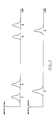
- the detectors 56 and 60 each produce signals like those shown in the top waveform of Fig. 7. These signals are transmitted, via a line l53, to a computer 37 where they are analyzed in a manner explained hereinbelow in reference to Fig. 7.
- Fig. 4 shows a plan view of a section of a typical first level reticle 82 of Fig. l. Shown is a circuit pattern l30 under which the circuit pattern l04 of Fig. 2 is exposed.
- the apertures l3l and l32 pass the exposing light 90 to expose the alignment target ll0 of Fig. 2.
- apertures l33 and l34 are useful in exposing an alignment target l05, also shown in Fig. 2.
- Fig. 5 shows a plan view of a section of a typical second level reticle 82 useful in the apparatus of Fig. l.
- Fig. 5 also illustrates the first level reticle targets l39-l42.
- the reticle targets l39-l42 comprise two reticle target slits each.
- the reticle target slits are narrow transmitting windows and modulate the light as the reticle 82 scans across the light reflected by the wafer 86. This light is re-imaged by a condenser relay 88 at a plane 9l. The light then passes through a dichroic mirror 92.
- the dichroic mirror 92 directs illumination light 90 into the optical system of Fig. l to expose the wafer 86.
- Such exposure illumination 90 does not form a part of the present invention.
- the exposure illumination 90 does, however, provide light that passes through the reticle slits l39-l42 in the reticle 82. This light is imaged on the wafer 86 as reticle slit images l43-l46 shown in Fig. 6.
- the reticle slit images l43-l46 consist of narrow (l ⁇ m at the wafer) line segments which straddle the wafer targets lll and ll2, as shown in Fig. 6 when the reticle 82 is properly aligned to the wafer 86.
- the reticle slit images l43-l46 are made to straddle the wafer target to reduce errors caused by imperfect orientation of the slit mask 22 with respect to the same direction, shown by arrow ll8 in Fig. 6. It should be noted that the dimensions shown in Fig. 6 are for the purpose of example only.
- the image ll4 and ll5 of the slit mask 22 on the wafer 86 overlays the area described by the reticle slit images l43-l46. It is light from the laser l0, reflected from the area of the slit images l43-l46, that is modulated by the reticle slits l39-l42.
- the condition shown in Fig. 6, with the slit images l43 and l44 co-linear with wafer target lll and slit images l45 and l46 co-linear with wafer target ll2 represents perfect wafer-to-reticle alignment.
- Also shown in Fig. 6 are the next level wafer targets l48 and l49 as printed by radiation passing through apertures l35 and l36.
- the light that passes through the dichroic mirror 92 is focused onto a detector l02 by a lens 96.
- a filter 94 is provided to filter out all but the wavelength of interest. That is, one of the wavelengths produced by the laser l0.
- a dichroic mirror similar in construction and use to dichroic mirror 50, could also be provided to allow for viewing multiple wavelengths.
- An optional aperture stop 98 shown in the optical system and in plan view in Fig. l, can be employed to further block stray light in the manner described hereinabove in reference to the aperture stop 44.
- the detector l02 receives the light signal as modulated by the reticle slits l39-l42.
- the signal generated by the detector l02 in response to the light thereon is shown as the lower waveform in Fig. 7. It is transmitted,. via a line l5l, to the computer 37 where it is processed in the manner described hereinbelow in reference to Fig. 7
- Items 9l-l02 are applicable to just one field position on the wafer 86, as are items 30-78 and 36-60.
- the beamsplitter 26 sends light from the laser l0 to another similar set of optics for detection of a row of targets, such as l05 in Fig. 2, at another field location on the wafer 86.
- Alignment error information can be extracted from the comparison of t3 - t2 with t2 - t1 for -45° targets and t6 - t5 with t5 - t4 for +45° targets.
- the separation between the slit images ll4 and ll5 is made different from the separation between wafer targets lll and ll2 to ensure that the signal peaks from the -45° bar, at t1 and t3, are easily distinguished from those of the +45° bar, at t4 and t6. Furthermore the slit images ll4 and ll5 are longer than the distance spanned by the reticle slit images to ensure that the entire reticle target is illuminated.
- the X and Y deviation of the reticle from the wafer can be determined as can magnification errors and rotation of the reticle relative to the wafer.
- the magnitude of the X and Y deviation of the reticle from the wafer and the magnification error is computed in the computer 37 through techniques known in the art. If a correction is needed a correction signal is sent from the computer 37, via a line l62, to correction actuators l60 and l54.
- a wafer actuator l60 and a reticle actuator l54 correct the relative positions of the wafer 86 and reticle 82, respectively, through mechanical linkages l58 and l52, respectively, acting on a wafer supporting platform l56 and a reticle supporting platform l50 respectively.
- a plurality of targets may be fabricated on a single level of a semi-conductor product having many levels.
- the wafer-to-reticle alignment may be adjusted continuously as the wafer 86 and reticle 82 are scanned relative to the alignment light from the laser l0 and the exposure illumination l07 scans in the direction shown by an arrow l03 in Fig. 2.
- Fig. 8 shows another form of the alignment marks of Fig. 3 wherein there are two each of the -45° targets and of the +45° target. In this way one level can be aligned to a reticle through said wafer alignment marks l20 and l2l.
- the reticle images l43-l46 are printed on the scribe alley l08 co-linear with the wafer marks l20 and l2l, as shown.
- No reticle marks are printed associated with wafer targets l22 or l23. Accordingly wafer targets l22 and l23 can be used later to align a subsequent circuit level to the one that was printed along with the wafer targets l22 and l23. In this way cumulative alignment errors can be avoided as circuit patterns are built up layer by layer.
- the system as described above utilizes reverse-dark-field wafer target detection and bright field reticle target detection.
- This system can be switched to reverse-bright-field wafer detection by a change of aperture stop 44 from the dark-field pattern 46 to the bright field pattern 48.
- the bright field patterns 48 blocks the scattered light and transmits the specularly reflected light from the wafer target ll0, shown in Fig. 2.
- the specularly reflected light has been greatly attenuated due to the low, e.g. l0% reflectivity of the central portion of the substrate 29, but the bright-field signal is generally stronger than the dark-field signal. This mode is useful in some cases when the reverse-dark-field wafer target signal is too weak or noisy.
- Both reticle and wafer target detection are performed separately and can be done at multiple wavelengths. If the signals at one wavelength are too small, they are ignored and signals at another wavelength are used. If more than one wavelength gives strong signals they can be averaged to yield more accurate data.
- the present invention does indeed provide a new and improved reverse dark-field reticle-to-wafer alignment system.
- This system aligns the reticle to the wafer during the scanning exposure process accurately and does so while the reticle and wafer are moving relative to the alignment illumination.
- Accurate wafer-to-reticle alignment is achieved by making use of the scanning motion required for scanning exposure, and without active scanning of the illumination light.
- the alignment can be accomplished even if there is relative motion between reticle and wafer as long as there is no relative motion between the wafer image and the reticle image, such as is the case in a scanning projection system with magnification other than unity.
Landscapes
- Physics & Mathematics (AREA)
- General Physics & Mathematics (AREA)
- Exposure And Positioning Against Photoresist Photosensitive Materials (AREA)
- Exposure Of Semiconductors, Excluding Electron Or Ion Beam Exposure (AREA)
- Container, Conveyance, Adherence, Positioning, Of Wafer (AREA)
- Length Measuring Devices By Optical Means (AREA)
Applications Claiming Priority (2)
| Application Number | Priority Date | Filing Date | Title |
|---|---|---|---|
| US06/868,506 US4697087A (en) | 1986-07-31 | 1986-07-31 | Reverse dark field alignment system for scanning lithographic aligner |
| US868506 | 1986-07-31 |
Publications (3)
| Publication Number | Publication Date |
|---|---|
| EP0254871A2 true EP0254871A2 (de) | 1988-02-03 |
| EP0254871A3 EP0254871A3 (en) | 1989-08-16 |
| EP0254871B1 EP0254871B1 (de) | 1993-05-19 |
Family
ID=25351825
Family Applications (1)
| Application Number | Title | Priority Date | Filing Date |
|---|---|---|---|
| EP87109074A Expired - Lifetime EP0254871B1 (de) | 1986-07-31 | 1987-06-24 | Umgekehrtes Dunkelfeld-Ausrichtsystem für einen lithographischen Ausrichtscanner |
Country Status (6)
| Country | Link |
|---|---|
| US (1) | US4697087A (de) |
| EP (1) | EP0254871B1 (de) |
| JP (1) | JP2634597B2 (de) |
| KR (1) | KR950007343B1 (de) |
| CA (1) | CA1252224A (de) |
| DE (1) | DE3785891T2 (de) |
Cited By (2)
| Publication number | Priority date | Publication date | Assignee | Title |
|---|---|---|---|---|
| GB2300275A (en) * | 1995-04-21 | 1996-10-30 | Nikon Corp | Controlling stages and scanning type exposure |
| US9001304B2 (en) | 2008-01-16 | 2015-04-07 | Carl Zeiss Smt Gmbh | Projection exposure system for microlithography with a measurement device |
Families Citing this family (23)
| Publication number | Priority date | Publication date | Assignee | Title |
|---|---|---|---|---|
| JPH021903A (ja) * | 1988-06-10 | 1990-01-08 | Mitsubishi Electric Corp | Ttlアライメント装置 |
| US5053628A (en) * | 1989-07-13 | 1991-10-01 | Matsushita Electric Industrial Co., Ltd. | Position signal producing apparatus for water alignment |
| JPH0430414A (ja) * | 1990-05-25 | 1992-02-03 | Matsushita Electric Ind Co Ltd | 位置決め装置 |
| US5206820A (en) * | 1990-08-31 | 1993-04-27 | At&T Bell Laboratories | Metrology system for analyzing panel misregistration in a panel manufacturing process and providing appropriate information for adjusting panel manufacturing processes |
| US5249069A (en) * | 1991-02-11 | 1993-09-28 | Eastman Kodak Company | Method and apparatus for automatic alignment of front and rear scanning cameras |
| JP2873410B2 (ja) * | 1991-02-25 | 1999-03-24 | 東京エレクトロン株式会社 | 被試料体の記号・文字識別装置 |
| US5469294A (en) * | 1992-05-01 | 1995-11-21 | Xrl, Inc. | Illumination system for OCR of indicia on a substrate |
| US5737122A (en) * | 1992-05-01 | 1998-04-07 | Electro Scientific Industries, Inc. | Illumination system for OCR of indicia on a substrate |
| JPH06310400A (ja) * | 1993-04-12 | 1994-11-04 | Svg Lithography Syst Inc | 軸上マスクとウェーハ直線配列システム |
| US5602619A (en) * | 1993-09-22 | 1997-02-11 | Nikon Precision, Inc. | Scanner for step and scan lithography system |
| JPH07270119A (ja) * | 1994-03-21 | 1995-10-20 | Nikon Corp | 集積回路リソグラフィー用の蛍光使用の直接レチクル対ウエハ・アライメントの方法及び装置 |
| US5751403A (en) * | 1994-06-09 | 1998-05-12 | Nikon Corporation | Projection exposure apparatus and method |
| US5477057A (en) * | 1994-08-17 | 1995-12-19 | Svg Lithography Systems, Inc. | Off axis alignment system for scanning photolithography |
| US5648854A (en) * | 1995-04-19 | 1997-07-15 | Nikon Corporation | Alignment system with large area search for wafer edge and global marks |
| KR100390818B1 (ko) * | 1996-06-28 | 2003-08-30 | 주식회사 하이닉스반도체 | 반도체균일패턴형성방법 |
| US5920396A (en) * | 1996-10-16 | 1999-07-06 | Svg Lithography Systems, Inc. | Line width insensitive wafer target detection |
| US5767523A (en) * | 1997-04-09 | 1998-06-16 | Svg Lithography Systems, Inc. | Multiple detector alignment system for photolithography |
| WO1999045580A1 (en) | 1998-03-06 | 1999-09-10 | Nikon Corporation | Exposure device and method of manufacturing semiconductor device |
| US6484060B1 (en) | 2000-03-24 | 2002-11-19 | Micron Technology, Inc. | Layout for measurement of overlay error |
| US6628406B1 (en) * | 2000-04-20 | 2003-09-30 | Justin L. Kreuzer | Self referencing mark independent alignment sensor |
| TWI264620B (en) * | 2003-03-07 | 2006-10-21 | Asml Netherlands Bv | Lithographic apparatus and device manufacturing method |
| US7511826B2 (en) * | 2006-02-27 | 2009-03-31 | Asml Holding N.V. | Symmetrical illumination forming system and method |
| WO2010091100A1 (en) | 2009-02-03 | 2010-08-12 | Abbott Cardiovascular Systems Inc. | Multiple beam laser system for forming stents |
Family Cites Families (7)
| Publication number | Priority date | Publication date | Assignee | Title |
|---|---|---|---|---|
| JPS5952535B2 (ja) * | 1977-01-21 | 1984-12-20 | キヤノン株式会社 | 光学装置 |
| JPS53135654A (en) * | 1977-05-01 | 1978-11-27 | Canon Inc | Photoelectric detecting device |
| JPS5534490A (en) * | 1978-09-01 | 1980-03-11 | Canon Inc | Alignment device |
| JPS57138134A (en) * | 1981-02-20 | 1982-08-26 | Nippon Kogaku Kk <Nikon> | Positioning device |
| JPS5874038A (ja) * | 1981-10-28 | 1983-05-04 | Canon Inc | マスクとウエハ−の位置合せ方法 |
| JPS5963504A (ja) * | 1982-10-02 | 1984-04-11 | Canon Inc | 位置合わせ信号検出装置 |
| JPS60188953A (ja) * | 1984-03-08 | 1985-09-26 | Canon Inc | 位置検出装置 |
-
1986
- 1986-07-31 US US06/868,506 patent/US4697087A/en not_active Expired - Lifetime
-
1987
- 1987-06-16 CA CA000539817A patent/CA1252224A/en not_active Expired
- 1987-06-24 EP EP87109074A patent/EP0254871B1/de not_active Expired - Lifetime
- 1987-06-24 DE DE8787109074T patent/DE3785891T2/de not_active Expired - Lifetime
- 1987-07-28 JP JP62186793A patent/JP2634597B2/ja not_active Expired - Lifetime
- 1987-07-29 KR KR1019870008239A patent/KR950007343B1/ko not_active Expired - Lifetime
Cited By (5)
| Publication number | Priority date | Publication date | Assignee | Title |
|---|---|---|---|---|
| GB2300275A (en) * | 1995-04-21 | 1996-10-30 | Nikon Corp | Controlling stages and scanning type exposure |
| US6285437B1 (en) | 1995-04-21 | 2001-09-04 | Nikon Corporation | Method for controlling stages, apparatus therefor, and scanning type exposure apparatus |
| US9001304B2 (en) | 2008-01-16 | 2015-04-07 | Carl Zeiss Smt Gmbh | Projection exposure system for microlithography with a measurement device |
| US9696639B2 (en) | 2008-01-16 | 2017-07-04 | Carl Zeiss Smt Gmbh | Projection exposure system for microlithography with a measurement device |
| US10042271B2 (en) | 2008-01-16 | 2018-08-07 | Carl Zeiss Smt Gmbh | Projection exposure system for microlithography with a measurement device |
Also Published As
| Publication number | Publication date |
|---|---|
| US4697087A (en) | 1987-09-29 |
| EP0254871B1 (de) | 1993-05-19 |
| CA1252224A (en) | 1989-04-04 |
| DE3785891T2 (de) | 1993-08-26 |
| JP2634597B2 (ja) | 1997-07-30 |
| KR880002243A (ko) | 1988-04-29 |
| EP0254871A3 (en) | 1989-08-16 |
| KR950007343B1 (ko) | 1995-07-10 |
| JPS6341023A (ja) | 1988-02-22 |
| DE3785891D1 (de) | 1993-06-24 |
Similar Documents
| Publication | Publication Date | Title |
|---|---|---|
| EP0254871A2 (de) | Umgekehrtes Dunkelfeld-Ausrichtsystem für einen lithographischen Ausrichtscanner | |
| US5202748A (en) | In situ process control system for steppers | |
| US4908656A (en) | Method of dimension measurement for a pattern formed by exposure apparatus, and method for setting exposure conditions and for inspecting exposure precision | |
| US5521036A (en) | Positioning method and apparatus | |
| JP2897276B2 (ja) | 位置合わせ方法及び露光装置 | |
| JP3128827B2 (ja) | 投影露光装置、並びに投影露光方法、及びその投影露光方法を用いたデバイス製造方法、及びそのデバイス製造方法により製造されたデバイス | |
| JPH07249558A (ja) | 位置合わせ方法 | |
| JPH0580497A (ja) | 面状態検査装置 | |
| JPH07123103B2 (ja) | 位置合わせ装置 | |
| JP5137526B2 (ja) | 形状測定装置、形状測定方法、および露光装置 | |
| JP2712330B2 (ja) | 露光条件測定方法 | |
| JP3230094B2 (ja) | 投影光学系の光学特性測定方法、光学特性測定装置、露光方法及びマスク | |
| JP3448673B2 (ja) | 投影露光装置 | |
| JP2006512760A (ja) | 照明系の性能測定方法 | |
| JPH04324615A (ja) | 位置合わせ装置及び位置合わせ方法 | |
| JPH06101427B2 (ja) | 露光装置 | |
| JPH0744138B2 (ja) | 位置合わせ装置 | |
| JPH0992591A (ja) | 位置合わせ方法 | |
| CA1193030A (en) | Alignment device for integrated circuit manufacturing machines | |
| JPH10172900A (ja) | 露光装置 | |
| JPS63221616A (ja) | マスク・ウエハの位置合わせ方法 | |
| JPH0612753B2 (ja) | パターン検出方法及びその装置 | |
| JP3295244B2 (ja) | 位置決め装置 | |
| JP2899026B2 (ja) | マーク検出装置 | |
| JP2550979B2 (ja) | アライメント方法 |
Legal Events
| Date | Code | Title | Description |
|---|---|---|---|
| PUAI | Public reference made under article 153(3) epc to a published international application that has entered the european phase |
Free format text: ORIGINAL CODE: 0009012 |
|
| AK | Designated contracting states |
Kind code of ref document: A2 Designated state(s): CH DE FR GB IT LI NL |
|
| PUAL | Search report despatched |
Free format text: ORIGINAL CODE: 0009013 |
|
| AK | Designated contracting states |
Kind code of ref document: A3 Designated state(s): CH DE FR GB IT LI NL |
|
| 17P | Request for examination filed |
Effective date: 19900216 |
|
| RAP1 | Party data changed (applicant data changed or rights of an application transferred) |
Owner name: SVG LITHOGRAPHY SYSTEMS, INC. |
|
| 17Q | First examination report despatched |
Effective date: 19920128 |
|
| ITF | It: translation for a ep patent filed | ||
| GRAA | (expected) grant |
Free format text: ORIGINAL CODE: 0009210 |
|
| AK | Designated contracting states |
Kind code of ref document: B1 Designated state(s): CH DE FR GB IT LI NL |
|
| REF | Corresponds to: |
Ref document number: 3785891 Country of ref document: DE Date of ref document: 19930624 |
|
| ET | Fr: translation filed | ||
| PLBE | No opposition filed within time limit |
Free format text: ORIGINAL CODE: 0009261 |
|
| STAA | Information on the status of an ep patent application or granted ep patent |
Free format text: STATUS: NO OPPOSITION FILED WITHIN TIME LIMIT |
|
| 26N | No opposition filed | ||
| PGFP | Annual fee paid to national office [announced via postgrant information from national office to epo] |
Ref country code: CH Payment date: 20010514 Year of fee payment: 15 |
|
| REG | Reference to a national code |
Ref country code: GB Ref legal event code: IF02 |
|
| PG25 | Lapsed in a contracting state [announced via postgrant information from national office to epo] |
Ref country code: LI Free format text: LAPSE BECAUSE OF NON-PAYMENT OF DUE FEES Effective date: 20020630 Ref country code: CH Free format text: LAPSE BECAUSE OF NON-PAYMENT OF DUE FEES Effective date: 20020630 |
|
| REG | Reference to a national code |
Ref country code: CH Ref legal event code: PL |
|
| PGFP | Annual fee paid to national office [announced via postgrant information from national office to epo] |
Ref country code: NL Payment date: 20060614 Year of fee payment: 20 |
|
| PGFP | Annual fee paid to national office [announced via postgrant information from national office to epo] |
Ref country code: GB Payment date: 20060615 Year of fee payment: 20 |
|
| PGFP | Annual fee paid to national office [announced via postgrant information from national office to epo] |
Ref country code: DE Payment date: 20060616 Year of fee payment: 20 |
|
| PGFP | Annual fee paid to national office [announced via postgrant information from national office to epo] |
Ref country code: FR Payment date: 20060619 Year of fee payment: 20 |
|
| PGFP | Annual fee paid to national office [announced via postgrant information from national office to epo] |
Ref country code: IT Payment date: 20060630 Year of fee payment: 20 |
|
| PG25 | Lapsed in a contracting state [announced via postgrant information from national office to epo] |
Ref country code: NL Free format text: LAPSE BECAUSE OF EXPIRATION OF PROTECTION Effective date: 20070624 |
|
| REG | Reference to a national code |
Ref country code: GB Ref legal event code: PE20 |
|
| NLV7 | Nl: ceased due to reaching the maximum lifetime of a patent |
Effective date: 20070624 |
|
| PG25 | Lapsed in a contracting state [announced via postgrant information from national office to epo] |
Ref country code: GB Free format text: LAPSE BECAUSE OF EXPIRATION OF PROTECTION Effective date: 20070623 |