EP0252734A2 - Verkleinerndes Projektionsbelichtungssystem des Reflexionstyps für Röntgenstrahlung - Google Patents
Verkleinerndes Projektionsbelichtungssystem des Reflexionstyps für Röntgenstrahlung Download PDFInfo
- Publication number
- EP0252734A2 EP0252734A2 EP87306037A EP87306037A EP0252734A2 EP 0252734 A2 EP0252734 A2 EP 0252734A2 EP 87306037 A EP87306037 A EP 87306037A EP 87306037 A EP87306037 A EP 87306037A EP 0252734 A2 EP0252734 A2 EP 0252734A2
- Authority
- EP
- European Patent Office
- Prior art keywords
- mask
- wafer
- rays
- mirror
- stage
- Prior art date
- Legal status (The legal status is an assumption and is not a legal conclusion. Google has not performed a legal analysis and makes no representation as to the accuracy of the status listed.)
- Granted
Links
Images


Classifications
-
- G—PHYSICS
- G02—OPTICS
- G02B—OPTICAL ELEMENTS, SYSTEMS OR APPARATUS
- G02B17/00—Systems with reflecting surfaces, with or without refracting elements
- G02B17/02—Catoptric systems, e.g. image erecting and reversing system
- G02B17/06—Catoptric systems, e.g. image erecting and reversing system using mirrors only, i.e. having only one curved mirror
- G02B17/0626—Catoptric systems, e.g. image erecting and reversing system using mirrors only, i.e. having only one curved mirror using three curved mirrors
- G02B17/0636—Catoptric systems, e.g. image erecting and reversing system using mirrors only, i.e. having only one curved mirror using three curved mirrors off-axis or unobscured systems in which all of the mirrors share a common axis of rotational symmetry
-
- B—PERFORMING OPERATIONS; TRANSPORTING
- B82—NANOTECHNOLOGY
- B82Y—SPECIFIC USES OR APPLICATIONS OF NANOSTRUCTURES; MEASUREMENT OR ANALYSIS OF NANOSTRUCTURES; MANUFACTURE OR TREATMENT OF NANOSTRUCTURES
- B82Y10/00—Nanotechnology for information processing, storage or transmission, e.g. quantum computing or single electron logic
-
- G—PHYSICS
- G03—PHOTOGRAPHY; CINEMATOGRAPHY; ANALOGOUS TECHNIQUES USING WAVES OTHER THAN OPTICAL WAVES; ELECTROGRAPHY; HOLOGRAPHY
- G03F—PHOTOMECHANICAL PRODUCTION OF TEXTURED OR PATTERNED SURFACES, e.g. FOR PRINTING, FOR PROCESSING OF SEMICONDUCTOR DEVICES; MATERIALS THEREFOR; ORIGINALS THEREFOR; APPARATUS SPECIALLY ADAPTED THEREFOR
- G03F7/00—Photomechanical, e.g. photolithographic, production of textured or patterned surfaces, e.g. printing surfaces; Materials therefor, e.g. comprising photoresists; Apparatus specially adapted therefor
- G03F7/20—Exposure; Apparatus therefor
- G03F7/2037—Exposure with X-ray radiation or corpuscular radiation, through a mask with a pattern opaque to that radiation
- G03F7/2039—X-ray radiation
-
- G—PHYSICS
- G03—PHOTOGRAPHY; CINEMATOGRAPHY; ANALOGOUS TECHNIQUES USING WAVES OTHER THAN OPTICAL WAVES; ELECTROGRAPHY; HOLOGRAPHY
- G03F—PHOTOMECHANICAL PRODUCTION OF TEXTURED OR PATTERNED SURFACES, e.g. FOR PRINTING, FOR PROCESSING OF SEMICONDUCTOR DEVICES; MATERIALS THEREFOR; ORIGINALS THEREFOR; APPARATUS SPECIALLY ADAPTED THEREFOR
- G03F7/00—Photomechanical, e.g. photolithographic, production of textured or patterned surfaces, e.g. printing surfaces; Materials therefor, e.g. comprising photoresists; Apparatus specially adapted therefor
- G03F7/70—Microphotolithographic exposure; Apparatus therefor
- G03F7/70008—Production of exposure light, i.e. light sources
- G03F7/70033—Production of exposure light, i.e. light sources by plasma extreme ultraviolet [EUV] sources
-
- G—PHYSICS
- G03—PHOTOGRAPHY; CINEMATOGRAPHY; ANALOGOUS TECHNIQUES USING WAVES OTHER THAN OPTICAL WAVES; ELECTROGRAPHY; HOLOGRAPHY
- G03F—PHOTOMECHANICAL PRODUCTION OF TEXTURED OR PATTERNED SURFACES, e.g. FOR PRINTING, FOR PROCESSING OF SEMICONDUCTOR DEVICES; MATERIALS THEREFOR; ORIGINALS THEREFOR; APPARATUS SPECIALLY ADAPTED THEREFOR
- G03F7/00—Photomechanical, e.g. photolithographic, production of textured or patterned surfaces, e.g. printing surfaces; Materials therefor, e.g. comprising photoresists; Apparatus specially adapted therefor
- G03F7/70—Microphotolithographic exposure; Apparatus therefor
- G03F7/70216—Mask projection systems
- G03F7/70233—Optical aspects of catoptric systems, i.e. comprising only reflective elements, e.g. extreme ultraviolet [EUV] projection systems
-
- G—PHYSICS
- G03—PHOTOGRAPHY; CINEMATOGRAPHY; ANALOGOUS TECHNIQUES USING WAVES OTHER THAN OPTICAL WAVES; ELECTROGRAPHY; HOLOGRAPHY
- G03F—PHOTOMECHANICAL PRODUCTION OF TEXTURED OR PATTERNED SURFACES, e.g. FOR PRINTING, FOR PROCESSING OF SEMICONDUCTOR DEVICES; MATERIALS THEREFOR; ORIGINALS THEREFOR; APPARATUS SPECIALLY ADAPTED THEREFOR
- G03F7/00—Photomechanical, e.g. photolithographic, production of textured or patterned surfaces, e.g. printing surfaces; Materials therefor, e.g. comprising photoresists; Apparatus specially adapted therefor
- G03F7/70—Microphotolithographic exposure; Apparatus therefor
- G03F7/70216—Mask projection systems
- G03F7/7025—Size or form of projection system aperture, e.g. aperture stops, diaphragms or pupil obscuration; Control thereof
-
- G—PHYSICS
- G03—PHOTOGRAPHY; CINEMATOGRAPHY; ANALOGOUS TECHNIQUES USING WAVES OTHER THAN OPTICAL WAVES; ELECTROGRAPHY; HOLOGRAPHY
- G03F—PHOTOMECHANICAL PRODUCTION OF TEXTURED OR PATTERNED SURFACES, e.g. FOR PRINTING, FOR PROCESSING OF SEMICONDUCTOR DEVICES; MATERIALS THEREFOR; ORIGINALS THEREFOR; APPARATUS SPECIALLY ADAPTED THEREFOR
- G03F7/00—Photomechanical, e.g. photolithographic, production of textured or patterned surfaces, e.g. printing surfaces; Materials therefor, e.g. comprising photoresists; Apparatus specially adapted therefor
- G03F7/70—Microphotolithographic exposure; Apparatus therefor
- G03F7/70691—Handling of masks or workpieces
-
- G—PHYSICS
- G03—PHOTOGRAPHY; CINEMATOGRAPHY; ANALOGOUS TECHNIQUES USING WAVES OTHER THAN OPTICAL WAVES; ELECTROGRAPHY; HOLOGRAPHY
- G03F—PHOTOMECHANICAL PRODUCTION OF TEXTURED OR PATTERNED SURFACES, e.g. FOR PRINTING, FOR PROCESSING OF SEMICONDUCTOR DEVICES; MATERIALS THEREFOR; ORIGINALS THEREFOR; APPARATUS SPECIALLY ADAPTED THEREFOR
- G03F7/00—Photomechanical, e.g. photolithographic, production of textured or patterned surfaces, e.g. printing surfaces; Materials therefor, e.g. comprising photoresists; Apparatus specially adapted therefor
- G03F7/70—Microphotolithographic exposure; Apparatus therefor
- G03F7/708—Construction of apparatus, e.g. environment aspects, hygiene aspects or materials
- G03F7/70858—Environment aspects, e.g. pressure of beam-path gas, temperature
- G03F7/70866—Environment aspects, e.g. pressure of beam-path gas, temperature of mask or workpiece
- G03F7/70875—Temperature, e.g. temperature control of masks or workpieces via control of stage temperature
-
- G—PHYSICS
- G03—PHOTOGRAPHY; CINEMATOGRAPHY; ANALOGOUS TECHNIQUES USING WAVES OTHER THAN OPTICAL WAVES; ELECTROGRAPHY; HOLOGRAPHY
- G03F—PHOTOMECHANICAL PRODUCTION OF TEXTURED OR PATTERNED SURFACES, e.g. FOR PRINTING, FOR PROCESSING OF SEMICONDUCTOR DEVICES; MATERIALS THEREFOR; ORIGINALS THEREFOR; APPARATUS SPECIALLY ADAPTED THEREFOR
- G03F7/00—Photomechanical, e.g. photolithographic, production of textured or patterned surfaces, e.g. printing surfaces; Materials therefor, e.g. comprising photoresists; Apparatus specially adapted therefor
- G03F7/70—Microphotolithographic exposure; Apparatus therefor
- G03F7/708—Construction of apparatus, e.g. environment aspects, hygiene aspects or materials
- G03F7/70858—Environment aspects, e.g. pressure of beam-path gas, temperature
- G03F7/70883—Environment aspects, e.g. pressure of beam-path gas, temperature of optical system
- G03F7/70891—Temperature
Definitions
- the present invention relates to a projection exposure apparatus, more particularly to an X-ray reduction projection exposure system of reflection type and an X-ray reduction imaging system particularly usable for effecting high resolution printing.
- the minimum line width which is printable by the apparatus is determined by wavelength of light used and a numerical aperture of the projection optical system.
- the resolution increases with increase of the numerical aperture, but the increase of the numerical aperture leads to shorter depth of focus, with the result that the image to be printed or transferred is blurred due to a very small defocusing. For this reason, it is considered from the standpoint of optical design that obtaining high resolution by changing the numerical aperture is difficult.
- efforts have been made to accomplish the high resolution by using as the projection energy ray a beam produced by excimer laser or the like and X-rays which are relatively short in the wavelength.
- the X-ray exposure apparatus is expected as an exposure apparatus of the next generation, and an X-ray exposure apparatus in a proximity type has been proposed.
- An X-ray reduction projection exposure system of reflection type and an X-ray reduction projection imaging system of reflection type not the conventional proximity type; an X-ray reduction projection exposure system of reflection type capable of printing images in the high resolution of the order of submicrons; an X-ray reduction projection exposure system of reflection type capable of effecting printing in a very high resolution; and a system comprising means for directing X-rays to a mask and a projection imaging system for forming an image of a mask pattern in a predetermined reduced magnification or scale. Therefore, the pattern of the mask can be transferred in a reduced scale onto a wafer disposed at an imaging position by way of a projection exposure system.
- an X-ray reduction projection imaging system of a reflection type according to a first embodiment of the present invention.
- an object plane is depicted by reference characters MS where a mask or the like is placed
- an image plane is depicted by reference characters WF where a wafer or the like is placed.
- the projection imaging system comprises reflection mirrors M1, M2 and M3 including a multi-layer film for reflecting X-rays to form an image in a reduced scale, the multi-layer film being designated by references R1, R2 and R3, respectively.
- the distances among those elements are indicated as follows:
- Those dimensions are the distances measured along an imaging axis O.
- the reduction projection imaging system of a reflection type shown in Figures 1 and 2 is structured by the concave reflecting mirror M1, the convex reflecting mirror M2 and the concave reflecting mirror M3, in the order named from the mask MS.
- the imaging system is effective to project in a reduced scale a circuit pattern of the mask MS onto the wafer WF, more particularly onto a resist applied on the surface of the wafer WF.
- the major specifications usually required for a projection imaging system performing the surface projection shown in Figure 1 and 4 in an exposure apparatus for producing an ultra LSI contain a ultra high resolution, a large size of image plane and no distortion. It is said that in the case of 64 megabits, the minimum line width of 0.35 micron and the image plane size of 28 ⁇ 10 mm2 are required, and that in the case of 256 megabits, the minimum line width of 0.25 micron and the image plane size of 40 ⁇ 20 mm2 are required. These requirements are generally contradictory to each other, and conventional imaging systems do not satisfy those requirements and specifications simultaneously.
- the projection imaging system of this embodiment makes it possible to satisfy those requirements.
- paraxial curvature radius r1, r2 and r3 of the concave mirror M1 the convex mirror M2 and the concave mirror M3 satisfy the following: 0.9 ⁇ r2/r1 + r2/r3 ⁇ 1.1 ...(1)
- those aberrations are corrected by reflecting the ray from the object by the concave mirror M1, the convex mirror M2 and the concave mirror M3 in this order, and by giving a function of an aperture stop to the convex mirror M2.
- at least one of the concave mirrors M1 and M3 and convex mirror M2 has aspherical or non-spherical mirror surface so as to further improve the correction of those aberrations.
- non-spherical surfaces of the concave mirrors M1 and M3 are desirable for improvement of imaging performance.
- the projection imaging system of Figure 1 has paraxial curvature radii of the concave mirrors M1 and M3 and the convex mirrors M2 which are determined so as to maintain small petzval sum, while the plane distances among the elements are so determined that the distortion is corrected, and the coma, astigmatism and spherical aberration are corrected by using the non-spherical surfaces.
- Figure 2 is a graph showing a relation between a geometrical aberration of an imaging system and an effective F-number.
- a lateral spherical aberration LSA is taken.
- F the effective F-number
- K a constant
- the constant K in effect means the value of the lateral spherical aberration when the effective F-number is 1.
- the value of the constant K changes depending on the number of lenses (mirrors) constituting the imaging system, the type of the imaging system and the design of the imaging system.
- a number of lenses (not less than 10) are used to accomplish the constant K of approximately l micron.
- the number of mirrors used is desirably as small as possible in order to increase the amount of usable rays as the rate absorbed by the mirror is large.
- the constant K is about 100 times the conventional, that is, the constant K is of the order of 100 microns.
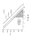
- Figure 3 is a graph representing the relation of the equation (3) in a log-log scale for three values of radii r0. According to this graph, when it is required that r0 ⁇ 0.35 micron, the combination of the effective F-number F and the wavelength ⁇ is selected within the region below the bottommost line.
- the imaging system is such that the geometric aberration shown in Figure 2 and the blurrness due to the diffraction shown in Figure 3 are both below the tolerances.
- the graph of Figure 2 gives F > 6.6, and therefore, the graph of Figure 3 gives the combination of the effective F-number and the wavelength within the hatched region.
- the imaging system of this embodiment uses a small number of mirrors, it is possible to reduce the geometrical aberrations and the blurrness due to diffraction down to not more than submicrons in the soft X-ray wavelength region.
- Figure 4 shows an arrangement, stressing the major parts of the imaging system of Figure 1, wherein the reflecting mirrors have multi-layer reflecting films.
- the reduction projection imaging system of a refraction type shown in Figures 1 and 4 are essentially coaxial imaging system, and only one half mirror surface of each of concave mirrors M1 and M3 are used. It is possible that at least one of the concave mirrors M1 and M3 and the convex mirror M2 is deviated from the coaxial relationship so as to slightly incline with respect to the system axis O, whereby further improving the correction of the aberrations.
- the image plane of the imaging system of Figure 4 is explained wherein the reference y represents an image height; y max , a maximum image height; y min , a minimum image height.
- the region y min ⁇ y ⁇ y max is used as the image plane or surface.
- the rays reaching to this region is substantially free from eclipse, and therefore, a uniform distribution of radiation amount can be provided with the vignetting factor of 100 %.
- the exemplary usable image plane has the maximum rectangular region under the condition that the ratio of the long side and the short side is 2:1.
- the various aberrations discussed above are satisfactorily corrected.
- the short side of the rectangular configuration is given by y max - y min
- the long side is given by
- the concave mirrors M1 and M3 and the convex mirror M2 of the Figure 4 projection imaging system have the respective reflecting surfaces coated with reflecting films for efficiently reflecting X-rays.
- Each of the reflecting films is constituted by several tens layers. The reflectivity is very much improved as compared with the reflecting mirror without the reflecting film.
- the multi-layer reflecting film may be constituted by a combination of such different materials that the difference in the refractive indexes of the adjacent layers is large, for example, a multi-layer film containing a semiconductor element and a transition metal element having a high fusing point, a multi-layer film containing a low fusing point metal element and a semiconductor element or a light metal element, or a multi-layer film containing white metal element and a semiconductor element.
- examples of combinations are tungsten W and carbon C; tantalum Ta and silicon Si; gold Au and carbon C; rhenium Re and carbon C; lead Pb and silicon Si; ruthenium Ru and silicon Si; paradium Pd and silicon Si; rhodium Rh and silicon Si; ruthenium Ru and beryllium Be; ruthenium Ru and boron B; rhodium Rh and boron B; palladium Pd and boron B.
- first material and “second material”.
- First Material Ru Second Material: Si Film Thickness of the 1st Mat.: 36.4 angstroms Film Thickness of the 2nd Mat.: 23.5 angstroms Number of Layers: 41 Reflectivity (Angle of incidence: 0 degree (perpendicular)): 38.6 %, without a protection film; 37.9 %, with a protection film of C having the thickness of 5 angstroms on the top layer.
- Second Material Si Film Thickness of the 1st Mat.: 39.1 angstroms Film Thickness of the 2nd Mat.: 25.2 angstroms Number of Layers: 41 Reflectivity (Angle of incidence: 20 degrees): 40.1 %, without a protection film; 39.4 %, with a protection film of C having the thickness of 5 angstroms on the top layer.
- First Material Pd Second Material: Si Film Thickness of the 1st Mat.: 31.3 angstroms Film Thickness of the 2nd Mat.: 28.0 angstroms Number of Layers: 41 Reflectivity (Angle of incidence: 0 degree): 26.1 %
- First Material Ru Second Material: Be Film Thickness of the 1st Mat.: 26.6 angstroms Film Thickness of the 2nd Mat.: 30.6 angstroms Number of Layers: 41 Reflectivity (Angle of incidence: 0 degree): 77.2 %
- First Material Ru Second Material: Be Film Thickness of the 1st Mat.: 27.4 angstroms Film Thickness of the 2nd Mat.: 33.4 angstroms Number of Layers: 41 Reflectivity (Angle of incidence: 20 degrees): 79.9 %
- Rh Second Material Si Film Thickness of the 1st Mat.: 33.4 angstroms Film Thickness of the 2nd Mat.: 23.4 angstroms Number of Layers: 41 Reflectivity (Angle of incidence: 0 degree): 33.2 %
- First Material Rh Second Material: Si Film Thickness of the 1st Mat.: 48.2 angstroms Film Thickness of the 2nd Mat.: 28.8 angstroms Number of Layers: 41 Reflectivity (Angle of incidence: 40 degrees): 38.7 %
- Second Material B Film Thickness of the 1st Mat.: 20.1 angstroms Film Thickness of the 2nd Mat.: 21.8 angstroms Number of Layers: 41 Reflectivity (Angle of incidence: 0 degree): 18.0 %
- First Material Ru Second Material: B Film Thickness of the 1st Mat.: 21.3 angstroms Film Thickness of the 2nd Mat.: 23.4 angstroms Number of Layers: 41 Reflectivity (Angle of incidence: 20 degrees): 21.6 %
- Rh Second Material B Film Thickness of the 1st Mat.: 20.0 angstroms Film Thickness of the 2nd Mat.: 21.9 angstroms Number of Layers: 41 Reflectivity (Angle of incidence: 0 degree): 15.7 %
- First Material Rh Second Material: B Film Thickness of the lst Mat.: 21.0 angstroms Film Thickness of the 2nd Mat.: 23.6 angstroms Number of Layers: 41 Reflectivity (Angle of incidence: 20 degrees): 18.8 %
- Rh Second Material B Film Thickness of the 1st Mat.: 19.4 angstroms Film Thickness of the 2nd Mat.: 22.4 angstroms Number of Layers: 41 Reflectivity (Angle of incidence: 0 degree): 13.2 %
- the multi-layer reflecting films described above are for the X-rays having the wavelength ranging from 80 - 120 angstroms. However, multi-layer reflecting films for the X-rays outside this range can be obtained by ordinary skilled in the art in consideration of the above by property selecting a combination of the above described materials.
- Each of the first and second materials is formed by a single element in the above examples, but it may be synthetic of plural elements.
- At least one of the concave mirrors M1 and M3 and the convex mirror M2 has a non-spherical reflecting surface, and therefore, in the examples which will be described has at least one non-spherical reflecting mirror.
- the concave mirrors M1 and M3 are substantially equidistant from the convex mirror M2.
- Examples 1-8 and 1-10 are suitable for manufacturing LSI of the order of 64 megabits.
- Example 1-9 is suitable for manufacturing LSI of the order of 256 megabits.
- the projection systems of embodiments 1-8 to 1-10 are relatively compact and of high resolution, but there is a liability that a slight distortion remains. If it remains, the distortion may be compensated by giving to the mask pattern itself the distortion opposite to the distortion not corrected by the projection imaging system.
- Examples 1-11 to 1-15 relate to the cases where the concave mirror M3 is disposed, with respect to travel of X-rays, between the concave mirror M1 and the convex mirror M2, wherein the concave mirror M3 is disposed spaced apart by approximately one half of the distance between the concave mirror M1 and the convex mirror M2.
- Examples 1-11 and 1-12 are for manufacturing LSI of the order of 64 megabits and 256 megabits, in which almost all distortions are substantially completely removed, and the effective F-number is 13 which means a light imaging system.
- the convex mirror M2 has a spherical surface and is designed for 64 megabit LSI.
- Example 1-14 has a projection magnification of 1/2 and is designed for 64 megabits LSI manufacturing.
- Example 1-15 has a unit projection magnification and is designed for 64 megabit LSI manufacturing.
- Examples 1-8 to 1-13 have the projection magnificaiton of 1/5. All the embodiments except for Example 1-13 has three mirrors M1, M2 and M3 all of which have non-spherical deflecting mirror surface.
- the projection imaging system described above employs three reflecting mirrors M1, M2 and M3.
- the projection system applicable to the projection exposure apparatus according to the present invention is not limited to the above-described detailed examples.
- an additional mirror that is, a fourth mirror M4 may be added.
- the multi-layer reflecting film is used as discussed above.
- the increase in the number of reflecting mirrors necessarily leads to loss of the X-ray.
- the number of the reflecting mirrors constituting the projection imaging or radiation system is preferably small.
- the projection imaging system have been described as being used for a plane projection, but the present invention is applicable to the case where a region of a predetermined image height range providing small aberration is projected through an arcuate slit or the like, and the mask and wafer are simultaneously scanningly moved so as to sequentially transfer the pattern.
- Figures 6 and 7 show aberrations in the Figure 1 projection imaging system and a fourth embodiment.
- a graph (A) represent an astigmatism
- graph (B) represent a distortion.
- graphs (A) - (D) represent lateral aberrations at different image height, (A) being for the image height of 185 mm; (B), 160 mm; (C), 130 mm; (D), 100 mm.
- the ordinate represents the image height.
- References M and S designate meridional surface and saggital surface, respectively.
- the aberration correction is satisfactory for the use of the projection imaging system of this kind.
- the distortion in Figure 6(B) is approximately 0, and therefore, the distortion is not shown in the Figure.
- the aberration correction can be made satisfactorily in such a wide range as to meet the imaging system applicable to plane projection exposure system, which necessiates a wide exposure area.
- the imaging system has a satisfactory MTF property sufficient to provide the resolution of the order of submicrons.
- Figure 8 explains the principle of the non-perpendicular incidence of illumination rays to the mask MS in Figures 1 and 4.
- the rays are incident perpendicularly to the wafer, that is, the illumination system is telecentric.
- the reflecting mirrors M1, M2 and M3 are generally indicated by reference MM; IP indicates a position of its entrance pupil; FF, front focus point; PL, a principal ray passing through the center of the mask MS and the front focal point FF.
- the ray from the center of the mask MS passes through the front focal point FF, and the marginal rays therearound pass through the entrance pupil.
- the rays L are inclinedly incident onto the mask MS.
- most of the rays are incident perpendicularly and/or substantially perpendicularly onto the wafer WF. This is preferable in the reflection system when only one half of the system arrangement above or below the system axis is used.
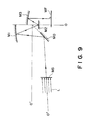
- Figure 9 shows an imaging arrangement of an X-ray reduction projection imaging system of a reflection type which is small in size, according to a second embodiment of the present invention.
- the rays from the mask MS toward the reflection mirror M1 are liable to be blocked at the time when an unshown wafer stage is moved in order to stepwisely expose each of the shot area of the wafer WF.
- the system arrangement of Figure 9 is intended to eliminate the liability.
- the system of this embodiment is provided with a fourth reflecting mirror M0.
- the movable range of the wafer WF is uninfluential to the imaging system.
- the reflecting mirror M0 may be inclined at an angle other than 45 degrees, although Figure 9 shows the example of 45 degrees.
- Second Material Si Film Thickness of the 1st Mat.: 55.4 angstroms Film Thickness of the 2nd Mat.: 34.3 angstroms Number of Layers: 41 Reflectivity (Angle of incidence: 45 degrees): 43.8 %
- First Material Pd Second Material: Si Film Thickness of the 1st Mat.: 44.5 angstroms Film Thickness of the 2nd Mat.: 42.3 angstroms Number of Layers: 41 Reflectivity (Angle of incidence: 45 degrees): 29.1 %
- Second Material Be Film Thickness of the 1st Mat.: 30.2 angstroms Film Thickness of the 2nd Mat.: 49.7 angstroms Number of Layers: 41 Reflectivity (Angle of incidence: 45 degrees): 85.3 %
- Second Material Si Film Thickness of the 1st Mat.: 52.7 angstroms Film Thickness of the 2nd Mat.: 31.9 angstroms Number of Layers: 41 Reflectivity (Angle of incidence: 45 degrees): 39.5 %
- Second Material B Film Thickness of the 1st Mat.: 27.6 angstroms Film Thickness of the 2nd Mat.: 32.8 angstroms Number of Layers: 41 Reflectivity (Angle of incidence: 45 degrees): 41.8 %
- Second Material B Film Thickness of the 1st Mat.: 26.7 angstroms Film Thickness of the 2nd Mat.: 33.5 angstroms Number of Layers: 41 Reflectivity (Angle of incidence: 45 degrees): 36.6 %
- First Material Pd Second Material: B Film Thickness of the 1st Mat.: 25.9 angstroms Film Thickness of the 2nd Mat.: 34.2 angstroms Number of Layers: 41 Reflectivity (Angle of incidence: 45 degrees): 30.2 %
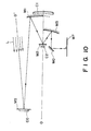
- Figure 10 illustrates a system arrangement of an X-ray reduction projection imaging system of a reflection type which is small in size according to a third embodiment of the present invention.
- the mask MS transmits the exposure rays
- the imaging system of Figure 10 uses a reflection type mask.
- This embodiment is preferable in that it matches in principle Figure 6 embodiment. This is because when a reflection type mask MS is used, the image rays of the circuit pattern of the mask on which the illumination rays are non-perpendicularly incident, can be efficiently introduced to the reflection mirror M1.
- the reflection type mask is preferable also in that a forced cooling means CO may be actable on the back side thereof, examples of the cooling means being a water cooling mechanism or electrostatic cooling mechanism using a Peltier element or the like.
- forced cooling means C1 and C2 or the like are provided for the reflection mirrors M1 and M2 or the like, since then the thermal expansion can be avoided.
- the cooling means can be provided for at least a few first reflection mirrors, and it is not necessary to provide it for the subsequent reflecting mirrors, because the liability of the high temperature is present in the first few mirrors.
- the cooling means can be provided for all of the reflecting mirrors. The non-perpendicular incidence of the rays onto the reflection type mask also applies advantageously to the imaging system shown in Figures 11, 12 and 13.
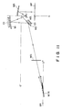
- Figure 11 shows an arrangement of an X-ray reduction projection imaging system of a reflection type which is small in size according to a fourth embodiment of the present invention.
- X-rays SR from a synchrotron orbital radiation source which will hereinafter be called "SOR" are reflected by reflection mirror MRT, and they are non-perpendicularly incident on the mask MS.
- the reflection mirror MTR is swung with respect to the mask MS to scan the circuit pattern surface of the mask MS thus insuring a wide exposure area.
- the reflecting mirror MTR may be of a glancing type or of a multi-layer type. In this embodiment, too, it is preferable to provide the reflecting mirrors M0 and M1 forced cooling means.
- An X-ray conduit extending from SOR source is usually very long, extending in a tangential direction of a ring, and therefore, in the apparatus wherein the distance from the mask MS to the reflecting mirror M1 is long as in this embodiment, the conduit can be commonly used, thus preventing the apparatus from becoming bulky.
- Figure 12 shows an arrangement of an X-ray reduction projection imaging system of a reflection type which is small in size, according to a fifth embodiment of the present invention.
- the X-ray is scanningly deflected substantially vertically within the SOR source.
- the mask MS is set inclined from the vertical direction at a predetermined angle to provide non-perpendicular incidence of rays.
- Figure 13 shows a system arrangement of an X-ray reduction projection imaging system of a reflection type which is small in size, according to a sixth embodiment of the present invention.
- the mask MS and the wafer WF are disposed vertically and parallel to each other, wherein the illumination rays are still unblocked. Therefore, this arrangement is suitable to the apparatus wherein the wafer is moved stepwisely to expose plural shot areas of the wafer.
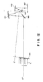
- Figure 14 shows a general arrangement of an exposure apparatus according to a seventh embodiment of the present invention.
- the mask MS is disposed vertically so as to suitably meet the SOR source.
- the wafer WF is supported on a horizontal stage, and as to the imaging system, the reflection imaging system of Figure 9, 11 or 12 can be used.
- a mask stage MS for supporting the mask MS is movable in two dimensions by an unshown driving device.
- the mask stage 1 is provided thereon with alignment marks 2A, 2B and 2C, which are exposed at different three positions on the mask stage l as shown in the Figure in this embodiment.
- the alignment marks are used to detect the degree of perpendicularity between the mask MS and the wafer WF and/or the wafer stage.
- the apparatus comprises a conduit tube in which the X-ray passes and which is effective to direct the X-ray emitted from an unshown X-ray source and having passed through the mask MS to a projection imaging system which will be described hereinafter.
- a barrel 4 for accommodating the projection imaging system comprising a plurality of reflecting mirrors and is connected with the conduit tube 3.
- First, second and third stage alignment scopes 10, 11 and 12 are effective to observe the alignment marks 2A, 2B and 2C and alignment marks 6A, 6B and 6C on the member 50, respectively superimposedly.
- First and second mask-wafer alignment scopes 20 and 21 function to detect alignment or deviation between the mask MS and the wafer WF to impart a relative movement between the mask MS and the wafer WF using the corresponding alignment marks on the mask MS and the wafer WF.
- the system comprises the above-described multi-layer film reflecting mirrors M0, M1, M2 and M3. Of these mirrors, the mirrors M1, M2 and M3 constitute a reduction projection imaging system; and the reflection mirror M0 serves to fold the X-ray introduced into the barrel 4 through the conduit tube 3 from the inlet port thereof to the reflecting mirror M1 at a predetermined angle.
- the reflecting mirror M3 is provided with an opening h1 for allowing passage of the X-ray at an eccentric position.
- the opening h1 is formed prior to the multi-layer film treatment, and is plugged by a material, under which condition the multi-layer film is formed. After the completion of the multi-layer film treatment, the material filling the opening is removed. By doing so, the distortion which may otherwise be produced during the machining of the opening can be avoided.
- the reflecting mirror M2 is securedly fixed onto a supporting plate SS having the opening h2.
- Members 50, 51 and 52 are stage constituent members for constituting a wafer stage.
- the constituent member 50 is provided with a wafer chuck for securedly supporting the wafer WF.
- the top surface of the constituent member 50 is provided with stage alignment mark 6A, 6B and 6C for alignment operation.
- the constituent member 51 carries the constituent member 50 and is movable on the constituent member 52 in the X direction as shown in the Figure.
- the constituent member 52 is movable in Y direction as indicated in the Figure, so that the constituent members 51 and 52 constitute a so-called X-Y stage.
- driving devices 70 and 71 are provided, which include step motors respectively.
- the constituent member 50 is rotatable in ⁇ direction by an unshown driving device.
- the constituent member 50 is vertically movable by piezoelectric elements P1, P2 and P3 disposed there-below as shown in Figure 15.
- Distance meters 90, 91 and 92 for controlling the stage are provided to detect the position and movement amount of the wafer in the X and Y directions with high precision.
- a non-contact type optical type
- interferometer type is preferable.
- the projection exposure apparatus shown in Figure 14 is such that an image of the pattern of the mask MS is projected as a plane projection onto the wafer by forming a reduced image thereof by the reflecting mirror M1, M2 and M3, and the exposure is effected for each of chips or for a group of plural chips defined by scribe lines on the wafer WF, that is, in a so-called step-and-repeat fashion.
- the mask MS is supported by an unshown mask holder on the mask stage 1, while the wafer WF is attracted on an unshown wafer chuck. After completion of an alignment operation between the wafer WF and the mask MS which will be described hereinafter, the exposure operation is executed in the following manner.
- the X-ray emitted from the unshown X-ray source illuminates the mask MS, and the circuit pattern of the mask MS is formed on the wafer WF in a predetermined region through the conduit tube 3, the reflection mirror M0 and a reduction projection system comprising reflecting mirrors M1, M2 and M3.
- the information representative of the circuit pattern of the mask MS is transmitted onto the wafer WF in the form of a strength distribution of an X-ray, and a latent image of a circuit pattern is formed in the photosensitive material (resist) for the X-ray applied on the surface of the wafer WF.
- the wavelength range of the used X-ray may be selected in harmonization with the properties of the photosensitive layer and the projection system.
- the mask MS may be illuminated through an X-ray filter having a desired absorption property, such as BN (boron nitride).
- a desired absorption property such as BN (boron nitride).
- the driving devices 70 and 71 drive the wafer stage comprising the constituent members 50, 51 and 52, so that the alignment marks 6A, 6B and 6C on the constituent member 50 can be sequentially observed by stage alignment scope 10, 11 and 12 through the projection imaging system including the reflecting mirror M1, M2 and M3.
- a semiconductor laser head LZ mounted to the bottom face of the supporting plate SS is actuated to emit light.
- the stage is driven so as to face the alignment mark 6A on the wafer stage to the opening h2.
- the focus detection is effected between the alignment mark 2A on the mask stage 1 and the alignment mark 6A on the wafer stage using the alignment scope 12.
- the wafer stage is driven vertically to provide a focused stage by the piezoelectric element P1.
- the marks 6B and 6C are sequentially faced to the opening h2, the focus condition is detected using the marks 2B and 2C and alignment scopes 11 and 10, and the piezoelectric elements P2 and P3 are actuated so as to vertically move the wafer stage.
- the respective distances between three marks 2A, 2B and 2C and three marks 6A, 6B and 6C are adjusted to a focused state.
- the degree of perpendicularity between the mask stage and the wafer stage are assured.
- the X and Y direction deviations are sequentially measured and memorized using the marks 2A, 2B and 2C and the marks 6A, 6B and 6C. It is possible that the correcting drive may be executed using the motors 70 and 71.
- the perpendicularity correction is advantageous between the mask MS and the wafer WF.
- the mask MS and the wafer WF are adjusted to be parallel to each other in the imaging systems shown in Figures 1, 4, 8 and 13. Since the alignment marks 6A, 6B and 6C on the wafer stage are detected by the beam inversely travelling the reduction imaging system, and therefore, if the reduction is 1/5, the alignment marks 6A, 6B and 6C can be detected in an enlarged scale, that is 5 times.
- the information regarding the alignment from the alignment scopes 10, 11 and 12 can be obtained visually or photo-electrically.
- any of known methods may be used.
- a positional relationship is predetermined between such an area of the exposure region of the wafer WF retained on the constituent member 50 that is to be exposed to the pattern by a first shot (for example, the area for a first chip defined by orthogonal scribe lines) and the alignment marks 6A, 6B and 6C
- the wafer stage including the constituent members 50, 51 and 52 are moved, after the above described stage alignment operation, on the basis of the predetermined positional relationship so that the first shot area on the wafer WF is brought to the neighborhood of the image area of the projection imaging system where the pattern of the mask MS is formed.
- a predetermined couple of alignment marks is formed at the marginal area of the first shot exposure area on the wafer WF.
- These alignment marks and unshown alignment marks on the mask MS are visually or photoelectrically detected using the mask-wafer alignment scopes 20 and 21, so that a further highly accurate alignment can be exposed.
- the semiconductor laser head LZ functioning as the light source for the alignment produces light having the wavelength of for example 780 nm - 850 nm it is noted that the wavelength is longer than the wavelength of 100 angstroms of the exposure X-ray by 1 - 2 orders.
- the reflecting surfaces of the multi-layer film reflecting mirror can effectively reflect the laser beam as by a simple metal layer reflecting surface.
- the alignment marks on the wafer stage or the wafer WF are observed in an enlarged scale, for example, 5 times, if the reduction ratio of the reduction reflection system is 1/5, since the light travels inversely by way of the reflecting mirrors M3, M2 and M1 toward the mask MS.
- the reflecting mirror does not essentially exhibit wavelength dependence on the wavelength of this order, and therefore, a highly accurate alignment can be maintained so that it is preferable.
- the exposure step which has been described hereinbefore starts. If the positional relationship between the first shot area and the subsequent step-and-repeat areas, and the sequence of the exposures are stored in an unshown control device, the movement to the next shot area subsequent to the first shot can be performed through the control device to move the wafer stage with high precision (step movement) without the alignment operation between the mask MS and the wafer WF for each shot.
- the system wherein the alignment operation is carried out only for the first shot, and the subsequent stepwise movement for the remaining shots are effected trusting the mechanical accuracy of the stage is more preferable than a die-by-die alignment wherein the alignment is performed between the mask MS and the wafer WF for each of the shots.
- the inside of the projection exposure apparatus shown in Figure 14 is evacuated since the X-ray is used for the exposure.
- evacuating means such as a vacuum pump (not shown) is used to evacuate it to such an extent of vacuum of 10 ⁇ 6 Torr.
- the degree of vacuum in the apparatus is preferably higher, and in this embodiment, the exposure is performed under high vacuum or ultra high vacuum condition.
- the above described reflecting mirror cooling means is advantageous.
- the air in the apparatus containing N2 and O2 and others is replaced by light elements such as H and/or He so as to fill the inside of the apparatus with light element or elements for the exposure of X-rays.
- the front side (X-ray receiving side) of the mask MS in Figure 14 and the backside thereof (inside the barrel 3) and the upper surface of the wafer WF are all covered and filled with He flowing at a constant speed. Then, those light elements hardly absorb the X-ray, while on the other hand, they exhibit better heat absorption than the vacuum, so that the mask MS and the reflecting mirror are protected from distortion due to heat.
- the number of X-ray transmitting window covered by beryllium can be minimized so as to minimize the attenuation of the X-ray energy, in other words, to efficiently use the X-ray.
- the upper portion of the mask MS is in a He chamber
- the lower barrel 3 is a vacuum chamber
- the upper portion of the wafer is in an air chamber
- the Be window is required for each of the boundaries, resulting in large attenuation of the X-ray energy. Since H is very easy to burn, He is better from the standpoint of safety. Even when the He is used, the mirror or mirrors may be provided with forced cooling means.
- the X-ray used for the exposure When the wavelength of the X-ray used for the exposure is large, the X-ray is easily absorbed by various materials, and therefore the possibility of influence to the human body or the like is very small, and the X-rays hardly leak externally by employing the shield for maintaining the vacuum. On the other hand, with the decrease of the wavelength of the X-ray, the absorption thereof by various materials becomes smaller, and therefore, it is preferable to provide a shield for the X-ray as the case may be depending on the wavelength of the X-ray used.
- a pattern of the mask illuminated by the X-rays is imaged on the wafer by way of the projection imaging system to expose the wafer to the pattern, and the projection imaging system formed the image in a reduced scale, so that the precision required for the mask pattern is eased as compared with the conventional proximity method, thus making the manufacturing of the mask easier.
- the reduction projection enhances the resolution.
- the latitude to the usable X-ray source is increased, so that the applicability is enhanced.
- the necessity for the accurate gap measurement between the mask and the wafer which is needed in the proximity method and for the adjustment of the gap is eliminated.
- the X-ray mask usable with the present invention may be of a transparent type or a reflection type.
- the transparent type X-ray mask includes an X-ray absorbing portion and a mask substrate for supporting the X-ray absorbing portion, the X-ray absorbing portion forming a pattern on the mask substrate.
- the X-ray absorbing portion may be of Au, Pa, W or the like which exhibit high X-ray absorbing rate and which is easy to process.
- the material of the mask substrate organic high molecular materials and inorganic materials are usable.
- the former there are polyimide, Myler and Kapton and as to the latter, there are Si, Bn, Ti, Si3N4, SiC and Si in which B is dispersed.
- SiN substrate and a compound substrate of polyimide and Bn are usable.
- the reflection type X-ray mask includes a mask substrate having low reflectivity on which a pattern is drawn with high reflectivity material.
- a mask substrate having low reflectivity on which a pattern is drawn with high reflectivity material.
- a pattern is drawn by high electron density material (heavy element substance) such as Au or the like, or as another example, a multi-layer reflecting film including Ti and Ni is patterned on a mask substrate.
- the mask MS to be used with the present invention is required to be selected depending on the wavelength of the X-ray used. For example, if the wavelength of the X-ray to be used is several angstroms TO several tens angstroms, the material of the mask may be selected from the above-described. However, if the wavelength is relatively long, for example, several tens angstrom to several hundreds angstroms, the above-described materials are not preferable since they absorb much X-ray energy. For the masks for the long wavelength X-rays, several tens angstroms - several hundreds angstroms, through openings are formed in the X-ray absorbing member and reflecting member in accordance with the circuit pattern, that constituting a mask.
- a conventional X-ray source of so-called electron beam excitation type wherein an electron beam is applied to a solid metal to produce X-rays an X-ray source utilizing laser plasma, rare gas plasma, cleeping discharge plasma or a source utilizing synchrotron radiation represented by SOR (synchrotron orbital radiation).
- the X-ray sensitive material used for the exposure that is, the resist, can be selected from wide range of materials from high sensitivity to a relatively low sensitivity materials depending on the energy density of the exposure X-ray which is different is the X-ray is different.
- negative type X-ray resist material there are polyglycidylmethacrylate-CO-ethylacrylate (COP, maleic acid added polyglycidylmethacrylate (SEL-N), polydiallylorthophthalate, epoxidized polybutadiene, polystyrene TIF, metallic salt containing resist material, halogen containing polyvinyl ether resist material and halogen containing polyacrylate resist material.
- COP polyglycidylmethacrylate-CO-ethylacrylate
- SEL-N maleic acid added polyglycidylmethacrylate
- SEL-N polydiallylorthophthalate
- epoxidized polybutadiene polystyrene TIF
- metallic salt containing resist material metallic salt containing resist material
- halogen containing polyvinyl ether resist material halogen containing polyacrylate resist material
- positive type X-ray resist materials there are polymethyl methacrylate (PMMA), polyhexafluorobutylmethacrylate, polytetrafluoropropylmethacrylate, polymethacrylonitrile, poly(MMA-CO-trichloroethylmethacrylate), polybutene-1-sulfone, metallic acid containing resist material, polytrichloromethacrylate, polymethylmethacrylate-CO-dimethylmethylenemalonate (PMA-CO-DMM), copolymer of n-hexyl aldehyde and n-butyl aldehyde, and polychloroacetaldehyde.
- PMMA polymethyl methacrylate
- PMA-CO-DMM polymethylmethacrylate-CO-dimethylmethylenemalonate
- copolymer of n-hexyl aldehyde and n-butyl aldehyde and polychloroacetaldehyde
- the loss of the X-ray energy by the mirror surfaces and the distortion of the reflecting mirror by the heat can be minimized, and therefore, the exposure pattern transfer can be performed efficiently and with high resolution.
Priority Applications (1)
| Application Number | Priority Date | Filing Date | Title |
|---|---|---|---|
| EP99201981A EP0947882B1 (de) | 1986-07-11 | 1987-07-08 | Verkleinerndes Projektionsbelichtungssystem des Reflexionstyps für Röntgenstrahlung |
Applications Claiming Priority (21)
| Application Number | Priority Date | Filing Date | Title |
|---|---|---|---|
| JP61163068A JP2603225B2 (ja) | 1986-07-11 | 1986-07-11 | X線投影露光装置及び半導体製造方法 |
| JP163068/86 | 1986-07-11 | ||
| JP16306886 | 1986-07-11 | ||
| JP148616/87 | 1987-06-15 | ||
| JP14861187 | 1987-06-15 | ||
| JP14861587 | 1987-06-15 | ||
| JP62148615A JP2711537B2 (ja) | 1987-06-15 | 1987-06-15 | X線露光装置 |
| JP148615/87 | 1987-06-15 | ||
| JP14861387 | 1987-06-15 | ||
| JP148614/87 | 1987-06-15 | ||
| JP14861687 | 1987-06-15 | ||
| JP148613/87 | 1987-06-15 | ||
| JP62148612A JP2628164B2 (ja) | 1987-06-15 | 1987-06-15 | 露光装置 |
| JP14861487 | 1987-06-15 | ||
| JP62148613A JP2673517B2 (ja) | 1987-06-15 | 1987-06-15 | 露光装置 |
| JP62148611A JP2556328B2 (ja) | 1987-06-15 | 1987-06-15 | 露光装置 |
| JP62148614A JP2628165B2 (ja) | 1987-06-15 | 1987-06-15 | X線露光装置 |
| JP62148616A JPS63311315A (ja) | 1987-06-15 | 1987-06-15 | 物体・像変換装置 |
| JP148612/87 | 1987-06-15 | ||
| JP14861287 | 1987-06-15 | ||
| JP148611/87 | 1987-06-15 |
Related Child Applications (1)
| Application Number | Title | Priority Date | Filing Date |
|---|---|---|---|
| EP99201981A Division EP0947882B1 (de) | 1986-07-11 | 1987-07-08 | Verkleinerndes Projektionsbelichtungssystem des Reflexionstyps für Röntgenstrahlung |
Publications (3)
| Publication Number | Publication Date |
|---|---|
| EP0252734A2 true EP0252734A2 (de) | 1988-01-13 |
| EP0252734A3 EP0252734A3 (de) | 1988-10-26 |
| EP0252734B1 EP0252734B1 (de) | 2000-05-03 |
Family
ID=27566131
Family Applications (2)
| Application Number | Title | Priority Date | Filing Date |
|---|---|---|---|
| EP99201981A Revoked EP0947882B1 (de) | 1986-07-11 | 1987-07-08 | Verkleinerndes Projektionsbelichtungssystem des Reflexionstyps für Röntgenstrahlung |
| EP87306037A Expired - Lifetime EP0252734B1 (de) | 1986-07-11 | 1987-07-08 | Verkleinerndes Projektionsbelichtungssystem des Reflexionstyps für Röntgenstrahlung |
Family Applications Before (1)
| Application Number | Title | Priority Date | Filing Date |
|---|---|---|---|
| EP99201981A Revoked EP0947882B1 (de) | 1986-07-11 | 1987-07-08 | Verkleinerndes Projektionsbelichtungssystem des Reflexionstyps für Röntgenstrahlung |
Country Status (3)
| Country | Link |
|---|---|
| US (1) | US5153898A (de) |
| EP (2) | EP0947882B1 (de) |
| DE (2) | DE3752314T2 (de) |
Cited By (26)
| Publication number | Priority date | Publication date | Assignee | Title |
|---|---|---|---|---|
| EP0279670A2 (de) * | 1987-02-18 | 1988-08-24 | Canon Kabushiki Kaisha | Reflexionsmaske |
| EP0368261A2 (de) * | 1988-11-07 | 1990-05-16 | Ultratech Stepper Inc. | Optisches System zur Wiedergabe im Massstab 1 : 1 |
| US5003567A (en) * | 1989-02-09 | 1991-03-26 | Hawryluk Andrew M | Soft x-ray reduction camera for submicron lithography |
| EP0422853A2 (de) * | 1989-10-13 | 1991-04-17 | AT&T Corp. | Vorrichtung für Halbleiterlithographie |
| EP0480617A2 (de) * | 1990-10-10 | 1992-04-15 | AT&T Corp. | Röntgenstrahllithographie mit ringförmigem Bildfeld |
| EP0523303A1 (de) * | 1991-07-19 | 1993-01-20 | AT&T Corp. | Lithographie mit ringförmigen Bildfeld |
| US5212588A (en) * | 1991-04-09 | 1993-05-18 | The United States Of America As Represented By The United States Department Of Energy | Reflective optical imaging system for extreme ultraviolet wavelengths |
| US5220590A (en) * | 1992-05-05 | 1993-06-15 | General Signal Corporation | X-ray projection lithography camera |
| EP0600708A1 (de) * | 1992-12-01 | 1994-06-08 | Canon Kabushiki Kaisha | Reflexionsmaske und deren Verwendung zur Herstellung von Mikrovorrichtungen |
| US5338647A (en) * | 1990-03-16 | 1994-08-16 | Fujitsu Limited | Reflection type photomask and reflection type photolithography method comprising a concavo-convex surface |
| US5353322A (en) * | 1992-05-05 | 1994-10-04 | Tropel Corporation | Lens system for X-ray projection lithography camera |
| EP0532236B1 (de) * | 1991-09-07 | 1997-07-16 | Canon Kabushiki Kaisha | System zur Stabilisierung der Formen von optischen Elementen, Belichtungsvorrichtung unter Verwendung dieses Systems und Verfahren zur Herstellung von Halbleitervorrichtungen |
| EP0883029A1 (de) * | 1997-06-05 | 1998-12-09 | Nikon Corporation | Belichtungsapparat |
| EP0957402A2 (de) * | 1998-05-15 | 1999-11-17 | Asm Lithography B.V. | Lithographische Vorrichtung |
| WO2000038017A1 (en) * | 1998-12-21 | 2000-06-29 | The Regents Of The University Of California | Projection optics box or assembly |
| EP1107066A2 (de) * | 1999-12-03 | 2001-06-13 | Asm Lithography B.V. | Lithographischer Apparat mit einer Maskenklemmvorrichtung |
| EP1229573A1 (de) * | 1999-07-16 | 2002-08-07 | Nikon Corporation | Belichtungsverfahren und -system |
| US6459472B1 (en) | 1998-05-15 | 2002-10-01 | Asml Netherlands B.V. | Lithographic device |
| US6465272B1 (en) | 1999-07-22 | 2002-10-15 | Corning Incorporated | Extreme ultraviolet soft x-ray projection lithographic method and mask devices |
| EP1367425A2 (de) * | 2002-05-31 | 2003-12-03 | Sony Corporation | Lichtabtastvorrichtung und Abbildungsvorrichtung für zweidimensionale Bilder |
| US6710917B2 (en) | 2000-10-20 | 2004-03-23 | Carl Zeiss Smt Ag | 8-mirror microlithography projection objective |
| US6776006B2 (en) | 2000-10-13 | 2004-08-17 | Corning Incorporated | Method to avoid striae in EUV lithography mirrors |
| US6867913B2 (en) | 2000-02-14 | 2005-03-15 | Carl Zeiss Smt Ag | 6-mirror microlithography projection objective |
| US6950809B2 (en) | 2000-03-03 | 2005-09-27 | Dun & Bradstreet, Inc. | Facilitating a transaction in electronic commerce |
| US7177076B2 (en) | 2000-10-20 | 2007-02-13 | Carl Zeiss Smt Ag | 8-mirror microlithography projection objective |
| CN103487923A (zh) * | 2013-09-17 | 2014-01-01 | 中国科学院西安光学精密机械研究所 | 一种全反射光学成像系统 |
Families Citing this family (71)
| Publication number | Priority date | Publication date | Assignee | Title |
|---|---|---|---|---|
| JPH04333011A (ja) * | 1991-05-09 | 1992-11-20 | Nikon Corp | 反射縮小投影光学装置 |
| JP3127511B2 (ja) * | 1991-09-19 | 2001-01-29 | 株式会社日立製作所 | 露光装置および半導体装置の製造方法 |
| US5214685A (en) * | 1991-10-08 | 1993-05-25 | Maxwell Laboratories, Inc. | X-ray lithography mirror and method of making same |
| US5581605A (en) * | 1993-02-10 | 1996-12-03 | Nikon Corporation | Optical element, production method of optical element, optical system, and optical apparatus |
| US5361292A (en) * | 1993-05-11 | 1994-11-01 | The United States Of America As Represented By The Department Of Energy | Condenser for illuminating a ring field |
| US5410434A (en) * | 1993-09-09 | 1995-04-25 | Ultratech Stepper, Inc. | Reflective projection system comprising four spherical mirrors |
| JP3666951B2 (ja) * | 1995-10-06 | 2005-06-29 | キヤノン株式会社 | マーク検出方法、これを用いた位置合わせ方法、露光方法及び装置、ならびにデバイス生産方法 |
| US5805365A (en) * | 1995-10-12 | 1998-09-08 | Sandia Corporation | Ringfield lithographic camera |
| US6521101B1 (en) * | 1995-11-04 | 2003-02-18 | The Regents Of The University Of California | Method for fabricating beryllium-based multilayer structures |
| US5815310A (en) * | 1995-12-12 | 1998-09-29 | Svg Lithography Systems, Inc. | High numerical aperture ring field optical reduction system |
| JP3814359B2 (ja) | 1996-03-12 | 2006-08-30 | キヤノン株式会社 | X線投影露光装置及びデバイス製造方法 |
| JP3862347B2 (ja) * | 1996-04-11 | 2006-12-27 | キヤノン株式会社 | X線縮小露光装置およびこれを利用したデバイス製造方法 |
| US6051344A (en) * | 1997-06-17 | 2000-04-18 | Intel Corporation | Multiple reduction photolithography technique |
| US5956192A (en) * | 1997-09-18 | 1999-09-21 | Svg Lithography Systems, Inc. | Four mirror EUV projection optics |
| DE19741492A1 (de) * | 1997-09-19 | 1999-03-25 | Microparts Gmbh | Verfahren zur Herstellung von Mikrostrukturkörpern |
| US6081578A (en) * | 1997-11-07 | 2000-06-27 | U.S. Philips Corporation | Three-mirror system for lithographic projection, and projection apparatus comprising such a mirror system |
| US6199991B1 (en) | 1997-11-13 | 2001-03-13 | U.S. Philips Corporation | Mirror projection system for a scanning lithographic projection apparatus, and lithographic apparatus comprising such a system |
| AU1053199A (en) | 1997-11-14 | 1999-06-07 | Nikon Corporation | Exposure apparatus and method of manufacturing the same, and exposure method |
| US6014252A (en) * | 1998-02-20 | 2000-01-11 | The Regents Of The University Of California | Reflective optical imaging system |
| US5973826A (en) * | 1998-02-20 | 1999-10-26 | Regents Of The University Of California | Reflective optical imaging system with balanced distortion |
| US6226346B1 (en) | 1998-06-09 | 2001-05-01 | The Regents Of The University Of California | Reflective optical imaging systems with balanced distortion |
| AU2549899A (en) * | 1998-03-02 | 1999-09-20 | Nikon Corporation | Method and apparatus for exposure, method of manufacture of exposure tool, device, and method of manufacture of device |
| US6577443B2 (en) | 1998-05-30 | 2003-06-10 | Carl-Zeiss Stiftung | Reduction objective for extreme ultraviolet lithography |
| DE19923609A1 (de) * | 1998-05-30 | 1999-12-02 | Zeiss Carl Fa | Ringfeld-4-Spiegelsysteme mit konvexem Primärspiegel für die EUV-Lithographie |
| US6072852A (en) * | 1998-06-09 | 2000-06-06 | The Regents Of The University Of California | High numerical aperture projection system for extreme ultraviolet projection lithography |
| US6213610B1 (en) | 1998-09-21 | 2001-04-10 | Nikon Corporation | Catoptric reduction projection optical system and exposure apparatus and method using same |
| JP2002532895A (ja) | 1998-12-14 | 2002-10-02 | コーニンクレッカ フィリップス エレクトロニクス エヌ ヴィ | Euv照射システム |
| US6280906B1 (en) | 1998-12-22 | 2001-08-28 | U.S. Philips Corporation | Method of imaging a mask pattern on a substrate by means of EUV radiation, and apparatus and mask for performing the method |
| US7151592B2 (en) * | 1999-02-15 | 2006-12-19 | Carl Zeiss Smt Ag | Projection system for EUV lithography |
| US6985210B2 (en) * | 1999-02-15 | 2006-01-10 | Carl Zeiss Smt Ag | Projection system for EUV lithography |
| USRE42118E1 (en) * | 1999-02-15 | 2011-02-08 | Carl-Zeiss-Smt Ag | Projection system for EUV lithography |
| DE19910724A1 (de) | 1999-03-11 | 2000-09-14 | Zeiss Carl Fa | Mikrolithographie-Projektionsobjektiveinrichtung sowie Projektionsbelichtungsanlage |
| US6033079A (en) | 1999-03-15 | 2000-03-07 | Hudyma; Russell | High numerical aperture ring field projection system for extreme ultraviolet lithography |
| US6188513B1 (en) | 1999-03-15 | 2001-02-13 | Russell Hudyma | High numerical aperture ring field projection system for extreme ultraviolet lithography |
| EP1093021A3 (de) | 1999-10-15 | 2004-06-30 | Nikon Corporation | Projektionsbelichtungssystem sowie ein solches System benutzendes Gerät und Verfahren |
| TW508980B (en) | 1999-12-23 | 2002-11-01 | Koninkl Philips Electronics Nv | Method of generating extremely short-wave radiation, method of manufacturing a device by means of said radiation, extremely short-wave radiation source unit and lithographic projection apparatus provided with such a radiation source unit |
| US6304630B1 (en) | 1999-12-24 | 2001-10-16 | U.S. Philips Corporation | Method of generating EUV radiation, method of manufacturing a device by means of said radiation, EUV radiation source unit, and lithographic projection apparatus provided with such a radiation source unit |
| TW502559B (en) | 1999-12-24 | 2002-09-11 | Koninkl Philips Electronics Nv | Method of generating extremely short-wave radiation, method of manufacturing a device by means of said radiation, extremely short-wave radiation source unit and lithographic projection apparatus provided with such a radiation source unit |
| TW538256B (en) | 2000-01-14 | 2003-06-21 | Zeiss Stiftung | Microlithographic reduction projection catadioptric objective |
| JP2001272358A (ja) * | 2000-03-24 | 2001-10-05 | Nikon Corp | X線試料検査装置 |
| TW573234B (en) | 2000-11-07 | 2004-01-21 | Asml Netherlands Bv | Lithographic projection apparatus and integrated circuit device manufacturing method |
| JP2004514943A (ja) * | 2000-11-28 | 2004-05-20 | カール・ツアイス・エスエムテイ・アーゲー | 157nmリソグラフィ用の反射屈折投影系 |
| KR20020074232A (ko) * | 2000-12-06 | 2002-09-28 | 가부시키가이샤 니콘 | X선 투영 노광장치, x선 투영 노광방법 및 반도체디바이스 |
| JP3659175B2 (ja) * | 2001-02-16 | 2005-06-15 | 株式会社村田製作所 | 半導体チップの製造方法および半導体ウエハ |
| US6879374B2 (en) * | 2001-06-20 | 2005-04-12 | Asml Netherlands B.V. | Device manufacturing method, device manufactured thereby and a mask for use in the method |
| JP4178862B2 (ja) * | 2001-08-01 | 2008-11-12 | カール・ツァイス・エスエムティー・アーゲー | Euvフォトリソグラフィ用の反射投影レンズ |
| JP4639352B2 (ja) * | 2002-05-10 | 2011-02-23 | カール・ツァイス・エスエムティー・ゲーエムベーハー | 波長≦100nmで物体を検査する検査系 |
| US7022443B2 (en) * | 2003-02-12 | 2006-04-04 | Intel Corporation | Compensation of reflective mask effects in lithography systems |
| US7158215B2 (en) * | 2003-06-30 | 2007-01-02 | Asml Holding N.V. | Large field of view protection optical system with aberration correctability for flat panel displays |
| US8208198B2 (en) | 2004-01-14 | 2012-06-26 | Carl Zeiss Smt Gmbh | Catadioptric projection objective |
| US7760327B2 (en) * | 2003-10-02 | 2010-07-20 | Carl Zeiss Smt Ag | Reflecting optical element with eccentric optical passageway |
| US7466489B2 (en) * | 2003-12-15 | 2008-12-16 | Susanne Beder | Projection objective having a high aperture and a planar end surface |
| JP5102492B2 (ja) | 2003-12-19 | 2012-12-19 | カール・ツァイス・エスエムティー・ゲーエムベーハー | 結晶素子を有するマイクロリソグラフィー投影用対物レンズ |
| US7463422B2 (en) * | 2004-01-14 | 2008-12-09 | Carl Zeiss Smt Ag | Projection exposure apparatus |
| US20080151365A1 (en) | 2004-01-14 | 2008-06-26 | Carl Zeiss Smt Ag | Catadioptric projection objective |
| DE602005008707D1 (de) * | 2004-01-14 | 2008-09-18 | Zeiss Carl Smt Ag | Catadioptrisches projektionsobjektiv |
| US7712905B2 (en) | 2004-04-08 | 2010-05-11 | Carl Zeiss Smt Ag | Imaging system with mirror group |
| KR20170129271A (ko) | 2004-05-17 | 2017-11-24 | 칼 짜이스 에스엠티 게엠베하 | 중간이미지를 갖는 카타디옵트릭 투사 대물렌즈 |
| US20080112927A1 (en) * | 2006-10-23 | 2008-05-15 | Genegrafts Ltd. | Cells and methods utilizing same for modifying the electrophysiological function of excitable tissues |
| EP1930771A1 (de) * | 2006-12-04 | 2008-06-11 | Carl Zeiss SMT AG | Projektionsobjektive mit Spiegelelementen mit Reflexbeschichtungen |
| JP5018787B2 (ja) * | 2006-12-27 | 2012-09-05 | 旭硝子株式会社 | Euvリソグラフィ用反射型マスクブランク |
| WO2008093534A1 (ja) * | 2007-01-31 | 2008-08-07 | Asahi Glass Company, Limited | Euvリソグラフィ用反射型マスクブランク |
| US8027022B2 (en) | 2007-07-24 | 2011-09-27 | Carl Zeiss Smt Gmbh | Projection objective |
| KR101393999B1 (ko) | 2007-08-20 | 2014-05-14 | 칼 짜이스 에스엠티 게엠베하 | 반사 코팅을 갖는 미러 소자들을 구비하는 투영 대물렌즈 |
| WO2009060549A1 (ja) * | 2007-11-09 | 2009-05-14 | Nalux Co., Ltd. | 結像光学系および距離測定装置 |
| DE102009054869B4 (de) | 2009-04-09 | 2022-02-17 | Carl Zeiss Smt Gmbh | Spiegel zur Führung eines Strahlungsbündels, Vorrichtungen mit einem derartigen Spiegel sowie Verfahren zur Herstellung mikro- oder nanostrukturierter Bauelemente |
| DE102009047179B8 (de) * | 2009-11-26 | 2016-08-18 | Carl Zeiss Smt Gmbh | Projektionsobjektiv |
| DE102014204171A1 (de) | 2014-03-06 | 2015-09-24 | Carl Zeiss Smt Gmbh | Optisches Element und optische Anordnung damit |
| CN109425977B (zh) * | 2017-08-24 | 2021-12-24 | 坦前科技股份有限公司 | 抬头显示器的光学反射模组 |
| JP7228966B2 (ja) * | 2018-06-29 | 2023-02-27 | キヤノン株式会社 | 画像処理装置及びその制御方法及びプログラム |
| CN109298605A (zh) * | 2018-11-30 | 2019-02-01 | 上海华力微电子有限公司 | 像差校正系统、光刻机及像差校正方法 |
Citations (1)
| Publication number | Priority date | Publication date | Assignee | Title |
|---|---|---|---|---|
| US4226501A (en) * | 1978-10-12 | 1980-10-07 | The Perkin-Elmer Corporation | Four mirror unobscurred anastigmatic telescope with all spherical surfaces |
Family Cites Families (15)
| Publication number | Priority date | Publication date | Assignee | Title |
|---|---|---|---|---|
| US3527526A (en) * | 1965-05-26 | 1970-09-08 | Ernest W Silvertooth | Catoptric image-forming system in which light is reflected twice from each surface |
| US3748015A (en) * | 1971-06-21 | 1973-07-24 | Perkin Elmer Corp | Unit power imaging catoptric anastigmat |
| US4302079A (en) * | 1980-04-10 | 1981-11-24 | Bell Telephone Laboratories, Incorporated | Photolithographic projection apparatus using light in the far ultraviolet |
| JPS57106031A (en) * | 1980-12-23 | 1982-07-01 | Toshiba Corp | Transferring device for fine pattern |
| JPS58101426A (ja) * | 1981-12-11 | 1983-06-16 | Nec Corp | X線露光装置 |
| EP0121412B1 (de) * | 1983-03-29 | 1991-11-27 | Kabushiki Kaisha Toshiba | Verfahren für die Herstellung mittels Projektion einer integrierten Schaltungsabbildung auf einer Halbleiterplatte |
| JPS6093410A (ja) * | 1983-10-27 | 1985-05-25 | Canon Inc | 反射光学系 |
| JPS60173551A (ja) * | 1984-02-20 | 1985-09-06 | Hideki Matsumura | X線など光線の反射投影によるパタ−ン転写法 |
| JPS612124A (ja) * | 1984-06-14 | 1986-01-08 | Canon Inc | 結像光学系 |
| US4682037A (en) * | 1984-07-10 | 1987-07-21 | Canon Kabushiki Kaisha | Projection exposure apparatus having an alignment light of a wavelength other than that of the exposure light |
| JPS6134941A (ja) * | 1984-07-26 | 1986-02-19 | Canon Inc | 合焦検知装置 |
| US4701035A (en) * | 1984-08-14 | 1987-10-20 | Canon Kabushiki Kaisha | Reflection optical system |
| US4748477A (en) * | 1985-04-30 | 1988-05-31 | Canon Kabushiki Kaisha | Exposure apparatus |
| US4749867A (en) * | 1985-04-30 | 1988-06-07 | Canon Kabushiki Kaisha | Exposure apparatus |
| US5003567A (en) * | 1989-02-09 | 1991-03-26 | Hawryluk Andrew M | Soft x-ray reduction camera for submicron lithography |
-
1987
- 1987-07-08 EP EP99201981A patent/EP0947882B1/de not_active Revoked
- 1987-07-08 DE DE3752314T patent/DE3752314T2/de not_active Expired - Lifetime
- 1987-07-08 DE DE3752388T patent/DE3752388T2/de not_active Expired - Lifetime
- 1987-07-08 EP EP87306037A patent/EP0252734B1/de not_active Expired - Lifetime
-
1992
- 1992-02-28 US US07/841,298 patent/US5153898A/en not_active Expired - Lifetime
Patent Citations (1)
| Publication number | Priority date | Publication date | Assignee | Title |
|---|---|---|---|---|
| US4226501A (en) * | 1978-10-12 | 1980-10-07 | The Perkin-Elmer Corporation | Four mirror unobscurred anastigmatic telescope with all spherical surfaces |
Non-Patent Citations (10)
| Title |
|---|
| Applied Optics, vol.17, No.7, 1 April 1978, p.1072-1074, D.R.Shafer: "Four-mirror unobscured anastigmatic telescopes with all-spherical surfaces" * |
| Bulletin of the Electrotechnical Laboratory, vol. 49, No. 12, 1985, p. 47-54, K. Hoh et al.: "Feasibility Study on the Extreme UV/Soft X-Ray Projection-type Lithography" * |
| JOURNAL OF IMAGING SCIENCE, vol. 30, no. 2, March/April 1986, pages 80-86, Springfield, Virginia, US; F. CERRINA: "X-ray imaging with synchrotron radiation"* Page 85, right-hand column * * |
| JOURNAL OF OPTICS, vol. 15, no. 4A, September 1984, pages 270-280 Paris, FR; F. BRIDOU et al.: "Etude préliminaire d'objectifs catadioptriques a rayons x utilisant la réflextion totale ou les multicouches pour le diagnostic des plasmas" * Abstract; page 270, left-hand column page 25; figures 11,12 * * |
| JOURNAL OF VACUUM SCIENCE & TECHNOLOGY, vol. B3, no. 1, 2nd series, January/February 1985, pages 227-231 F.CERRINA et al.: "A synchrotron radiation x-ray lithography beam line of novel design" * Page 231, left-and column * * |
| N.T.I.S. TECHNICAL NOTES, no. 8, Part J, August 1984 page 590, Springfield, Virginia, US; J.H. UNDERWOOD et al.: "Normal-incidence soft-x.ray mirror" * Whole document * * |
| NUCLEAR INSTRUMENTS & METHODS IN PHYSICS RESEARCH, Section A, vol. A246, no. 1/3, May 1986, pages 437-439 North Holland Physics Publ. Div. NL; W. SCHILDKAMP et al.: "Helium cooling of x-ray optics during synchroton heating" * Abstract* * |
| REVIEW OF SCIENTIFIC INSTR. vol. 50, no. 4, April 1979, pages 510-512 New York, US; S. MARDIX et al.: "Image reduction to submicrometer dimensions by asymmetric crystal reflection of x-rays" * Abstract * * |
| Solid State Technology, June 1974, p.50-53, D.A.Markle: "A New Projection Printer" * |
| Solid State Technology, September 1984, p.159-166, D.A.Markle: "The Future and Potential of Optical Scanning Systems" * |
Cited By (43)
| Publication number | Priority date | Publication date | Assignee | Title |
|---|---|---|---|---|
| EP0279670A2 (de) * | 1987-02-18 | 1988-08-24 | Canon Kabushiki Kaisha | Reflexionsmaske |
| EP0279670A3 (de) * | 1987-02-18 | 1990-03-14 | Canon Kabushiki Kaisha | Reflexionsmaske |
| US5052033A (en) * | 1987-02-18 | 1991-09-24 | Canon Kabushiki Kaisha | Reflection type mask |
| EP0368261A2 (de) * | 1988-11-07 | 1990-05-16 | Ultratech Stepper Inc. | Optisches System zur Wiedergabe im Massstab 1 : 1 |
| EP0368261A3 (de) * | 1988-11-07 | 1991-09-04 | Ultratech Stepper Inc. | Optisches System zur Wiedergabe im Massstab 1 : 1 |
| US5003567A (en) * | 1989-02-09 | 1991-03-26 | Hawryluk Andrew M | Soft x-ray reduction camera for submicron lithography |
| EP0422853A2 (de) * | 1989-10-13 | 1991-04-17 | AT&T Corp. | Vorrichtung für Halbleiterlithographie |
| US5063586A (en) * | 1989-10-13 | 1991-11-05 | At&T Bell Laboratories | Apparatus for semiconductor lithography |
| EP0422853A3 (en) * | 1989-10-13 | 1991-12-18 | American Telephone And Telegraph Company | Apparatus for semiconductor lithography |
| US5338647A (en) * | 1990-03-16 | 1994-08-16 | Fujitsu Limited | Reflection type photomask and reflection type photolithography method comprising a concavo-convex surface |
| EP0480617A3 (en) * | 1990-10-10 | 1992-07-08 | American Telephone And Telegraph Company | X-ray ringfield lithography |
| EP0480617A2 (de) * | 1990-10-10 | 1992-04-15 | AT&T Corp. | Röntgenstrahllithographie mit ringförmigem Bildfeld |
| US5212588A (en) * | 1991-04-09 | 1993-05-18 | The United States Of America As Represented By The United States Department Of Energy | Reflective optical imaging system for extreme ultraviolet wavelengths |
| EP0523303A1 (de) * | 1991-07-19 | 1993-01-20 | AT&T Corp. | Lithographie mit ringförmigen Bildfeld |
| EP0532236B1 (de) * | 1991-09-07 | 1997-07-16 | Canon Kabushiki Kaisha | System zur Stabilisierung der Formen von optischen Elementen, Belichtungsvorrichtung unter Verwendung dieses Systems und Verfahren zur Herstellung von Halbleitervorrichtungen |
| US5220590A (en) * | 1992-05-05 | 1993-06-15 | General Signal Corporation | X-ray projection lithography camera |
| US5353322A (en) * | 1992-05-05 | 1994-10-04 | Tropel Corporation | Lens system for X-ray projection lithography camera |
| EP0600708A1 (de) * | 1992-12-01 | 1994-06-08 | Canon Kabushiki Kaisha | Reflexionsmaske und deren Verwendung zur Herstellung von Mikrovorrichtungen |
| US5503950A (en) * | 1992-12-01 | 1996-04-02 | Canon Kabushiki Kaisha | Reflection type mask and manufacture of microdevices using the same |
| EP0883029A1 (de) * | 1997-06-05 | 1998-12-09 | Nikon Corporation | Belichtungsapparat |
| EP0957402A2 (de) * | 1998-05-15 | 1999-11-17 | Asm Lithography B.V. | Lithographische Vorrichtung |
| US6459472B1 (en) | 1998-05-15 | 2002-10-01 | Asml Netherlands B.V. | Lithographic device |
| EP0957402B1 (de) * | 1998-05-15 | 2006-09-20 | ASML Netherlands B.V. | Lithographische Vorrichtung |
| WO2000038017A1 (en) * | 1998-12-21 | 2000-06-29 | The Regents Of The University Of California | Projection optics box or assembly |
| EP1229573A4 (de) * | 1999-07-16 | 2006-11-08 | Nikon Corp | Belichtungsverfahren und -system |
| EP1229573A1 (de) * | 1999-07-16 | 2002-08-07 | Nikon Corporation | Belichtungsverfahren und -system |
| US6576380B2 (en) | 1999-07-22 | 2003-06-10 | Corning Incorporated | Extreme ultraviolet soft x-ray projection lithographic method and mask devices |
| US6465272B1 (en) | 1999-07-22 | 2002-10-15 | Corning Incorporated | Extreme ultraviolet soft x-ray projection lithographic method and mask devices |
| EP1107066A3 (de) * | 1999-12-03 | 2004-12-15 | ASML Netherlands B.V. | Lithographischer Apparat mit einer Maskenklemmvorrichtung |
| EP1107066A2 (de) * | 1999-12-03 | 2001-06-13 | Asm Lithography B.V. | Lithographischer Apparat mit einer Maskenklemmvorrichtung |
| USRE41307E1 (en) | 1999-12-03 | 2010-05-04 | Asml Netherlands B.V. | Mask for clamping apparatus, e.g. for a lithographic apparatus |
| US6867913B2 (en) | 2000-02-14 | 2005-03-15 | Carl Zeiss Smt Ag | 6-mirror microlithography projection objective |
| US6950809B2 (en) | 2000-03-03 | 2005-09-27 | Dun & Bradstreet, Inc. | Facilitating a transaction in electronic commerce |
| US6776006B2 (en) | 2000-10-13 | 2004-08-17 | Corning Incorporated | Method to avoid striae in EUV lithography mirrors |
| US6710917B2 (en) | 2000-10-20 | 2004-03-23 | Carl Zeiss Smt Ag | 8-mirror microlithography projection objective |
| US7177076B2 (en) | 2000-10-20 | 2007-02-13 | Carl Zeiss Smt Ag | 8-mirror microlithography projection objective |
| US7372624B2 (en) | 2000-10-20 | 2008-05-13 | Carl Zeiss Smt Ag | 8-mirror microlithography projection objective |
| US7508580B2 (en) | 2000-10-20 | 2009-03-24 | Carl-Zeiss Smt Ag | 8-mirror microlithography projection objective |
| US6924936B2 (en) | 2002-05-31 | 2005-08-02 | Sony Corporation | Light scanning apparatus and two-dimensional image forming apparatus |
| EP1367425A2 (de) * | 2002-05-31 | 2003-12-03 | Sony Corporation | Lichtabtastvorrichtung und Abbildungsvorrichtung für zweidimensionale Bilder |
| EP1367425A3 (de) * | 2002-05-31 | 2004-08-18 | Sony Corporation | Lichtabtastvorrichtung und Abbildungsvorrichtung für zweidimensionale Bilder |
| CN103487923A (zh) * | 2013-09-17 | 2014-01-01 | 中国科学院西安光学精密机械研究所 | 一种全反射光学成像系统 |
| CN103487923B (zh) * | 2013-09-17 | 2015-09-02 | 中国科学院西安光学精密机械研究所 | 一种全反射光学成像系统 |
Also Published As
| Publication number | Publication date |
|---|---|
| EP0947882A3 (de) | 1999-10-13 |
| DE3752388D1 (de) | 2006-05-18 |
| DE3752388T2 (de) | 2006-10-19 |
| US5153898A (en) | 1992-10-06 |
| EP0947882B1 (de) | 2006-03-29 |
| DE3752314T2 (de) | 2000-09-14 |
| EP0252734A3 (de) | 1988-10-26 |
| EP0252734B1 (de) | 2000-05-03 |
| DE3752314D1 (de) | 2000-06-08 |
| EP0947882A2 (de) | 1999-10-06 |
Similar Documents
| Publication | Publication Date | Title |
|---|---|---|
| US5153898A (en) | X-ray reduction projection exposure system of reflection type | |
| US6727980B2 (en) | Apparatus and method for pattern exposure and method for adjusting the apparatus | |
| US6485153B2 (en) | Exposure apparatus and method | |
| US6014252A (en) | Reflective optical imaging system | |
| EP1260871A2 (de) | Verfahren und Vorrichtung zur Positionsdetektion, Belichtungsapparat und Verfahren zur Herstellung einer Vorrichtung | |
| JP2001217191A (ja) | リソグラフィ投影装置 | |
| US7626770B2 (en) | Illumination system with zoom objective | |
| EP1523699A2 (de) | Projektionsobjektiv für eine projektionsbelichtungsvorrichtung | |
| JPH09330878A (ja) | X線縮小露光装置およびこれを利用したデバイス製造方法 | |
| JP2003142363A (ja) | 位置合わせ装置、位置合わせ装置の制御方法、その位置合わせ装置を用いた投影露光装置、半導体デバイスの製造方法 | |
| JP2005317611A (ja) | 露光方法及び装置 | |
| EP1116072A1 (de) | Maske mit geringer thermischer verformbarkeit für euv-lithographie | |
| US20040125353A1 (en) | Projection optical system and exposure apparatus equipped with the projection optical system | |
| US7268855B2 (en) | Projection optical system | |
| JP2603225B2 (ja) | X線投影露光装置及び半導体製造方法 | |
| JP2673517B2 (ja) | 露光装置 | |
| JP2556328B2 (ja) | 露光装置 | |
| JP2711537B2 (ja) | X線露光装置 | |
| JPS63311315A (ja) | 物体・像変換装置 | |
| JP4366151B2 (ja) | 投影光学系、露光装置及びデバイスの製造方法 | |
| JP2628164B2 (ja) | 露光装置 | |
| JP2628165B2 (ja) | X線露光装置 | |
| JP2008258461A (ja) | 反射型縮小投影光学系、露光装置及びデバイスの製造方法 | |
| JPH07147230A (ja) | 縮小投影露光装置および半導体製造方法 | |
| JPH07146442A (ja) | 反射光学系 |
Legal Events
| Date | Code | Title | Description |
|---|---|---|---|
| PUAI | Public reference made under article 153(3) epc to a published international application that has entered the european phase |
Free format text: ORIGINAL CODE: 0009012 |
|
| AK | Designated contracting states |
Kind code of ref document: A2 Designated state(s): DE FR GB IT NL |
|
| PUAL | Search report despatched |
Free format text: ORIGINAL CODE: 0009013 |
|
| AK | Designated contracting states |
Kind code of ref document: A3 Designated state(s): DE FR GB IT NL |
|
| 17P | Request for examination filed |
Effective date: 19890317 |
|
| 17Q | First examination report despatched |
Effective date: 19910228 |
|
| GRAG | Despatch of communication of intention to grant |
Free format text: ORIGINAL CODE: EPIDOS AGRA |
|
| GRAG | Despatch of communication of intention to grant |
Free format text: ORIGINAL CODE: EPIDOS AGRA |
|
| GRAH | Despatch of communication of intention to grant a patent |
Free format text: ORIGINAL CODE: EPIDOS IGRA |
|
| GRAH | Despatch of communication of intention to grant a patent |
Free format text: ORIGINAL CODE: EPIDOS IGRA |
|
| GRAA | (expected) grant |
Free format text: ORIGINAL CODE: 0009210 |
|
| AK | Designated contracting states |
Kind code of ref document: B1 Designated state(s): DE FR GB IT NL |
|
| PG25 | Lapsed in a contracting state [announced via postgrant information from national office to epo] |
Ref country code: IT Free format text: LAPSE BECAUSE OF FAILURE TO SUBMIT A TRANSLATION OF THE DESCRIPTION OR TO PAY THE FEE WITHIN THE PRE;WARNING: LAPSES OF ITALIAN PATENTS WITH EFFECTIVE DATE BEFORE 2007 MAY HAVE OCCURRED AT ANY TIME BEFORE 2007. THE CORRECT EFFECTIVE DATE MAY BE DIFFERENT FROM THE ONE RECORDED.SCRIBED TIME-LIMIT Effective date: 20000503 Ref country code: FR Free format text: LAPSE BECAUSE OF FAILURE TO SUBMIT A TRANSLATION OF THE DESCRIPTION OR TO PAY THE FEE WITHIN THE PRESCRIBED TIME-LIMIT Effective date: 20000503 |
|
| REF | Corresponds to: |
Ref document number: 3752314 Country of ref document: DE Date of ref document: 20000608 |
|
| EN | Fr: translation not filed | ||
| PLBE | No opposition filed within time limit |
Free format text: ORIGINAL CODE: 0009261 |
|
| STAA | Information on the status of an ep patent application or granted ep patent |
Free format text: STATUS: NO OPPOSITION FILED WITHIN TIME LIMIT |
|
| 26N | No opposition filed | ||
| REG | Reference to a national code |
Ref country code: GB Ref legal event code: IF02 |
|
| PGFP | Annual fee paid to national office [announced via postgrant information from national office to epo] |
Ref country code: NL Payment date: 20060616 Year of fee payment: 20 |
|
| PGFP | Annual fee paid to national office [announced via postgrant information from national office to epo] |
Ref country code: GB Payment date: 20060717 Year of fee payment: 20 |
|
| PGFP | Annual fee paid to national office [announced via postgrant information from national office to epo] |
Ref country code: DE Payment date: 20060918 Year of fee payment: 20 |
|
| PG25 | Lapsed in a contracting state [announced via postgrant information from national office to epo] |
Ref country code: NL Free format text: LAPSE BECAUSE OF EXPIRATION OF PROTECTION Effective date: 20070708 |
|
| REG | Reference to a national code |
Ref country code: GB Ref legal event code: PE20 |
|
| NLV7 | Nl: ceased due to reaching the maximum lifetime of a patent |
Effective date: 20070708 |
|
| PG25 | Lapsed in a contracting state [announced via postgrant information from national office to epo] |
Ref country code: GB Free format text: LAPSE BECAUSE OF EXPIRATION OF PROTECTION Effective date: 20070707 |