EP0243771B1 - Procédé et dispositif de mesure accélérée et précise de la fréquence d'un signal - Google Patents
Procédé et dispositif de mesure accélérée et précise de la fréquence d'un signal Download PDFInfo
- Publication number
- EP0243771B1 EP0243771B1 EP87105445A EP87105445A EP0243771B1 EP 0243771 B1 EP0243771 B1 EP 0243771B1 EP 87105445 A EP87105445 A EP 87105445A EP 87105445 A EP87105445 A EP 87105445A EP 0243771 B1 EP0243771 B1 EP 0243771B1
- Authority
- EP
- European Patent Office
- Prior art keywords
- frequency
- pulses
- output
- signal
- input
- Prior art date
- Legal status (The legal status is an assumption and is not a legal conclusion. Google has not performed a legal analysis and makes no representation as to the accuracy of the status listed.)
- Expired - Lifetime
Links
Images
Classifications
-
- G—PHYSICS
- G01—MEASURING; TESTING
- G01R—MEASURING ELECTRIC VARIABLES; MEASURING MAGNETIC VARIABLES
- G01R23/00—Arrangements for measuring frequencies; Arrangements for analysing frequency spectra
- G01R23/02—Arrangements for measuring frequency, e.g. pulse repetition rate; Arrangements for measuring period of current or voltage
Definitions
- the invention is based on a method according to the preamble of claim 1.
- a method for measuring the frequency of a signal is already known, in which periods of the signal are counted over a predetermined period of time and the result is converted to a second.
- this method cannot be used for signals whose frequency is constantly changing unless you want to measure the average frequency.
- the inventive method with the characterizing features of claim 1 has the advantage that a frequency measurement of the intermediate frequency signal with extremely high resolution is possible using available electronic components.
- the method according to the invention is not limited to the measurement of intermediate frequency signals, but can also be used for other signals within the scope of the person skilled in the art. It also has the advantage that the measured value is available digitally as an output value and thus allows digital further processing of the signal.
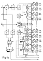
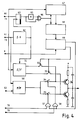
- the circuit arrangement according to FIG. 1 is supplied with a frequency-modulated intermediate frequency signal at 1, which is mixed in a mixing circuit with an IF carrier which is supplied at 3.
- a filter 4 connected to the mixing circuit 2
- the baseband which has a bandwidth of 150 kHz in VHF broadcasting is filtered out.
- This is fed to a limiter 5, at the output of which a rectangular signal is present, the frequency of which corresponds to the respective stroke of the frequency-modulated signal.
- clock pulses T1 are generated with the aid of a controllable oscillator (VCO) 6, which can be controlled by a frequency and phase comparator 7.
- VCO controllable oscillator
- the frequency and phase comparator 7 is supplied with a clock signal T4 at 8 with a reference frequency.
- the frequency of the clock pulses T1 emitted by the controllable oscillator 6 is 15.625 MHz.
- the clock pulses are passed over a runtime chain 100, which consists of 32 links 101 to 132. One link delays the clock pulses by 2 ns each.
- the clock T1 and the clock pulses which have passed through the entire delay chain 100 are fed to the frequency and phase comparator 7.
- the controllable oscillator 6 is controlled by comparing the delayed clock pulses T2 and the clock pulses T1 such that the period of the clock pulses T1 corresponds exactly to 32 times the delay of a link 101 to 132.
- the taps of the runtime chain 100 including its input and its output, thus have pulses which are each delayed by 2 ns to one another. These pulses are each fed to an input of one of the AND circuits 201 to 232.
- the output of the limiter 5 is supplied to the other inputs of the AND circuits 201 to 232.
- a pulse shaper 301 to 332 is connected to the outputs of the AND circuits 201 to 232. These each have two outputs, at which two time-shifted output pulses occur as a result of an input pulse. Since the clock pulses T1 are meandering, a pulse occurs alternately at the two outputs of each pulse shaper 301 to 332 at a distance of 32 ns - as long as the positive half-wave of the square-wave signal is present at the output of the limiter 5.
- the outputs of the pulse shapers 301 to 332 are denoted by 401 to 432 and 401 ⁇ to 432 ⁇ .
- the clock inputs of the counters are assigned to the outputs of pulse shapers 401 to 432 via OR circuits 51 to 58, which each have eight inputs A to H.
- the distribution of the count pulses 401 to 432 ⁇ takes place according to the scheme shown in Fig. 3 to the inputs A to H of the OR circuits 51 to 58.
- the division is made such that the count pulses at the inputs A to H of an OR gate always have the same distance and do not follow each other too closely, so that the clock limit frequency of the subsequent counter is not exceeded. Due to a larger number of OR circuits and counters, counters can also be used which are only suitable for lower clock frequencies.
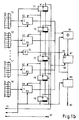
- the output signal of the limiter 5 is then equal to 0 - the measured value is to be formed from all counter readings.
- a summation of all meter readings must take place in the shortest possible time.
- the counter readings are switched through in succession to an adder.
- the outputs of the flip-flops 71 to 79 are connected to output registers of the counters 61 to 68.
- the outputs of the meters are low-impedance when switched through and otherwise high-impedance.
- the clock signal T3 for the shift register 71 to 79 is obtained with the frequency divider 81 from the clock pulses T1. As soon as the limited frequency-modulated intermediate frequency signal has become 0, the flip-flop 82 is set. The flip-flop 83 is then also set with the next clock pulse T3 and the clock for the shift registers 71 to 79 is thus released via the AND circuit 85.
- the last flip-flop 79 of the shift register no longer switches through the counter reading to the adder 86, but ends the summation by resetting the shift register 71 to 79 to the value 1, the two flip-flops 82, 83 and the counters 61 to 68 resets and transfers the value of the sum memory 87 into an output memory 89.
- the measurement result is then available in digital form at the output 90 of the output memory.
- the sum memory 87 is also deleted. For this purpose, a corresponding signal is fed from the output of the flip-flop 79 via a delay circuit 91 to a reset input 92 of the sum memory 87.
- the values in the output memory are inversely proportional to the FM frequency swing and are converted into values that are proportional to the frequency by creating reciprocal values. Since the sign of this difference is also important when measuring the frequency swing, ie the instantaneous deviation of the frequency of the modulated signal from the associated carrier, a sign bit is derived, as described below.
- both the carrier and the frequency-modulated signal are each fed via a limiter 93, 94 to a further frequency and phase comparator 95, with the two output signals of which a flip-flop 96 is controlled, at whose output 97 the sign bit can be tapped.
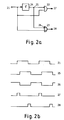
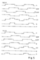
- FIG. 2a shows a block diagram of one of the pulse shapers and FIG. 2b shows diagrams of the signals occurring.
- the individual lines in FIG. 2b are provided with the same reference symbols as the circuit points in FIG. 2a at which the signals shown occur.
- the input 21 of the pulse shaper is connected to the output of one of the AND circuits 201 to 232 (FIG. 1a) and receives the meandering pulses shown in line 21 in FIG. 2b. These are each fed to an input of an AND circuit 22 and an OR circuit 23. In addition, they are delayed by a delay circuit 24 by a fraction of the period.
- the delayed meandering signals are shown in line 25 of FIG. 2b and are each fed to an inverting input of the AND circuit 22 and the NOR circuit 23.
- the inverted signal is shown in Fig. 2b, line 26.
- the AND operation of the signals according to line 21 and line 26 results in the pulses shown in line 27.
- the pulses shown in line 28 are created by NOR linking the same signals.
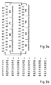
- the sequence in which the individual counting pulses occur is shown schematically in FIG. 3a.
- the counter pulses are compared to the inputs A to H of the OR circuits 51 to 58 shown in FIG. 1b.
- the counting impulses of the outputs 401 to 432 are contained in one cycle marked by arrows, while the inputs of the OR gates are shown in a second cycle which is run through with the same frequency.
- the table shown in FIG. 3b shows once again the assignment of the outputs of the pulse shapers 301 to 332 to the inputs of the OR circuits 51 to 58.
- Fig. 4 shows a block diagram of the frequency and phase comparator 7 (Fig. 1a).
- the desired frequency is first set (after switching on) with a frequency comparator .
- the phase at the input and output of the runtime chain is then regulated to 0 ° or 360 ° using a fast phase comparator. It is continuously checked whether the controllable oscillator has to be controlled with the frequency comparator or with the phase comparator.
- the signal T1 generated by the controllable oscillator 6 is fed via the input 41 to the circuit according to FIG. 2 and reaches a frequency divider 42.
- the output signal of the frequency divider 42 is mixed in a D flip-flop 43 with a reference signal T4 supplied at 44.
- a signal with the difference frequency is available at the output of the D flip-flop 43.
- a short pulse is derived from each positive and negative edge of this signal with the aid of the delay circuit 45 and the EXCL-OR circuit 46, which takes over the counter reading of a counter 47 into a memory 48 and then resets the counter 47.
- the counter 48 counts the clocks of the reference signal T4 in each case between adjacent pulses at the output of the EXCL-OR gate 46.
- the counter 48 counts up to an upper limit value, which prevents an overflow.
- the content of the memory 48 is compared with a predetermined value K in a comparator 49. If the content of the memory 48 is less than the value K, then the frequency comparator 31 is switched on, the switches 32 and 33 then being conductive, while the switches 34 and 35 being non-conductive. Otherwise, the phase comparator 50 is used.
- phase comparator 50 the output signal of which, if the phase position coincides, is 0 V and if there are deviations between the clock signals T1 and T2, positive or negative.
- the control voltage is fed to the controllable oscillator 6 (FIG. 1a) via an output stage 36.
- the runtime chain 100 contains taps in which the phase rotation of the signal T1 is 90 ° or 270 ° when the target frequency is present.
- These signals T1 / 90 ° and T1 / 270 ° determine after AND operations with the output signal of the phase comparator 50 (FIG. 4) in the circuit arrangement according to FIG. 4 via the AND gates 37 and 38, when the switches 34 and 35 are closed are provided that a corresponding signal is fed from the comparator 49 to the other inputs of the AND circuits 37 and 38, which means that the frequencies of the signals T1 and T4 differ only slightly from one another.
- signals appearing in the circuit arrangement are shown in FIG. 5. They are given the same name as those points of the circuit arrangement at which they occur. The signals are shown for two cases. In case A, the total delay of the runtime chain is small and in case B, the total delay is too large.
- the signal T1 / 2 is the output signal of a differential amplifier, which works as a phase comparator 50 (FIG. 4).
- the output voltage is negative if T1 is less than T2, zero if T1 is T2, and positive if T1 is greater than T2.
- the signal T1 / 2 is now AND-linked with the signals T1 / 90 ° and T1 / 270 °, the negative values of T1 / 2 being set to zero.
- the signals T1 / 2 + T1 / 90 ° abbreviated TX and T1 / 2 + T1 / 270 ° abbreviated TY arise, with which the gates 37 and 38 (FIG. 4) are controlled will.
Claims (9)
- Procédé de mesure de la fréquence d'un signal en comptant des impulsions de comptage dérivées d'impulsions d'horloge ou cadence et en émettant le résultat de comptage comme signal numérique, procédé caractérisé en ce que la fréquence des impulsions de comptage correspond à un multiple de la fréquence des impulsions d'horloge,- les impulsions de comptage apparaissant sur différentes prises d'une chaîne de temporisation (101-132),- le signal est limité dans un limiteur (50) pour que pendant une demi-onde du signal, le signal de sortie du limiteur (5) soit supérieur à zéro,- les impulsions de comptage sont comptées à l'aide de plusieurs compteurs (61-68) pendant une demi-onde et en ce qu'après cette demi-onde du signal, on réunit le contenu des compteurs (61-68) et on les transforme en une indication de fréquence appropriée en formant une valeur inverse.
- Procédé selon la revendication 1, caractérisé en ce que pour mesurer la fréquence d'un signal modulé en fréquence, on mélange celui-ci dans un mélangeur (2) à une porteuse appropriée.
- Procédé selon la revendication 2, caractérisé en ce que par comparaison de fréquence, et de phase du signal modulé en fréquence, limitée en amplitude dans un second limiteur (93), on déduit un signal de signe algébrique dans un comparaterur (95) par un troisième limiteur (94) à l'aide d'une porteuse limitée en amplitude.
- Circuit pour la mise en oeuvre du procédé selon la revendication 1, caractérisé en ce que la sortie d'un oscillateur (6) générant l'impulsion d'horloge est reliée à l'entrée de la chaîne de temporisation (100),- la chaîne de temporisation (100) comprend n éléments (101-132), n correspondant au rapport entre les fréquences des impulsions de comptage et les impulsions d'horloge,- l'entrée de la chaîne de temporisation (100) ainsi que les prises situées entre les éléments (101-132) sont respectivement reliées à une première entrée d'une porte ET (201-232),- les secondes entrées des portes ET (201-232) reçoivent une tension rectangulaire qui correspond à la fréquence du signal à mesurer,- les sorties des portes ET (201-232) sont reliées par des portes OU (51-58) aux entrées des compteurs (61-68) dont les sorties sont reliées à un circuit additionneur et de mise en mémoire (86, 87, 89).
- Circuit selon la revendication 4, caractérisé en ce qu'entre les sorties des portes ET (201-232) et les entrées des portes OU (51-58), on a chaque fois un formeur d'impulsions (301-332) qui fournit à une première sortie (401-432) des impulsions déclenchées par le flanc avant des impulsions appliquées et à une seconde sortie (401'-432'), les impulsions déclenchées par les flancs arrière.
- Circuit selon la revendication 4, caractérisé en ce que la fréquence de l'oscillateur (6) se commande à l'aide d'un comparateur de fréquence (31) et d'un comparateur de phase (50),- le comparateur de fréquence (31) fournit les impulsions d'horloge et un signal à la fréquence de référence,- le comparateur de phase (50) reçoit les impulsions d'horloge provenant respectivement de la sortie de l'oscillateur (6) et de la sortie de la chaîne de temps (100) et en ce qu'un circuit de commutation (31-35, 42-49) est prévu qui, en fonction de la différence entre la fréquence de référence et la fréquence d'horloge passant en-dessous d'une valeur prédéterminée, commute du comparateur de fréquence (31) sur le comparateur de phase (50).
- Circuit selon la revendication 4, caractérisé en ce que les sorties des compteurs (61-68) sont reliées par un commutateur cyclique au circuit d'addition et de mise en mémoire (86, 87, 89),- le commutateur reçoit les impulsions de commutation d'un diviseur de fréquence (81) par l'intermédiaire d'un montage à portes (82-85), l'entrée du diviseur de fréquence (81) étant reliée à la sortie de l'oscillateur (6) et,- le circuit de porte (81-85) est commandé de façon qu'à la fin d'un intervalle de temps à décompter, des impulsions de commutation soient transmises au commutateur et en ce que la transmission des impulsions de commutation ne se fait pas lorsque le commutateur a terminé un cycle de commutation.
- Circuit selon la revendication 7, caractérisé en ce que le commutateur est formé d'un registre à décalage (71-79) et des registres de sortie des compteurs (61-68),- les impulsions de commutation sont appliquées au registre à décalage comme horloge et en ce qu'une sortie d'un flip-flop formant le registre à décalage (71-72) est reliée aux entrées de remise à l'état initial des compteurs du registre à décalage et à l'entrée de commande du circuit de porte (82, 83, 85).
- Circuit selon la revendication 4, caractérisé en ce que le circuit d'addition et de mise en mémoire (86, 87, 89) est formé d'un additionneur (86), d'une mémoire d'addition (87) et d'une mémoire de sortie (89),- une entrée de l'additionneur (86) étant reliée par un commutateur aux sorties du compteur (61-68) et l'autre entrée de l'additionneur (86) étant reliée à une sortie de la mémoire d'addition (87),- la sortie de l'additionneur (86) est reliée à une entrée de la mémoire d'additionneur (87) et en ce que la sortie de la mémoire d'additionneur (87) est reliée à une entrée de la mémoire de sortie (89).
Priority Applications (1)
| Application Number | Priority Date | Filing Date | Title |
|---|---|---|---|
| AT87105445T ATE80952T1 (de) | 1986-04-26 | 1987-04-13 | Verfahren und anordnung zur schnellen und praezisen messung der frequenz eines signals. |
Applications Claiming Priority (2)
| Application Number | Priority Date | Filing Date | Title |
|---|---|---|---|
| DE3614272 | 1986-04-26 | ||
| DE19863614272 DE3614272A1 (de) | 1986-04-26 | 1986-04-26 | Verfahren und anordnung zur schnellen und praezisen messung der frequenz eines signals |
Publications (3)
| Publication Number | Publication Date |
|---|---|
| EP0243771A2 EP0243771A2 (fr) | 1987-11-04 |
| EP0243771A3 EP0243771A3 (en) | 1989-04-12 |
| EP0243771B1 true EP0243771B1 (fr) | 1992-09-23 |
Family
ID=6299662
Family Applications (1)
| Application Number | Title | Priority Date | Filing Date |
|---|---|---|---|
| EP87105445A Expired - Lifetime EP0243771B1 (fr) | 1986-04-26 | 1987-04-13 | Procédé et dispositif de mesure accélérée et précise de la fréquence d'un signal |
Country Status (6)
| Country | Link |
|---|---|
| US (1) | US4745356A (fr) |
| EP (1) | EP0243771B1 (fr) |
| JP (1) | JPS62261073A (fr) |
| AT (1) | ATE80952T1 (fr) |
| DE (2) | DE3614272A1 (fr) |
| ES (1) | ES2034976T3 (fr) |
Families Citing this family (6)
| Publication number | Priority date | Publication date | Assignee | Title |
|---|---|---|---|---|
| US4786861A (en) * | 1987-09-01 | 1988-11-22 | Sundstrand Data Control, Inc. | Frequency counting apparatus and method |
| DE3736124A1 (de) * | 1987-10-26 | 1989-05-03 | Licentia Gmbh | Verfahren und anordnung zur bestimmung der momentanfrequenz eines signals |
| DE3900292A1 (de) * | 1989-01-07 | 1990-07-12 | Acer Inc | Frequenzdetektor |
| US5610978A (en) * | 1994-12-30 | 1997-03-11 | Mitel Corporation | Ring discriminator |
| JP3691310B2 (ja) * | 1999-10-21 | 2005-09-07 | 富士通株式会社 | 周波数測定回路 |
| JP2021032761A (ja) * | 2019-08-27 | 2021-03-01 | セイコーエプソン株式会社 | 周波数計測回路及び周波数計測装置 |
Family Cites Families (5)
| Publication number | Priority date | Publication date | Assignee | Title |
|---|---|---|---|---|
| US3086172A (en) * | 1959-12-18 | 1963-04-16 | Gen Electric | Tunable filter arrangement |
| JPS526189B2 (fr) * | 1972-08-23 | 1977-02-19 | ||
| US4443766A (en) * | 1976-06-15 | 1984-04-17 | The United States Of America As Represented By The Secretary Of The Air Force | Precision digital sampler |
| DE2735785A1 (de) * | 1977-08-09 | 1979-02-22 | Bosch Gmbh Robert | Verfahren zur frequenzmessung unter verwendung digitaler schaltungsmittel |
| US4270209A (en) * | 1979-12-07 | 1981-05-26 | International Telephone And Telegraph Corporation | Digital compressive receiver |
-
1986
- 1986-04-26 DE DE19863614272 patent/DE3614272A1/de not_active Withdrawn
-
1987
- 1987-04-13 AT AT87105445T patent/ATE80952T1/de not_active IP Right Cessation
- 1987-04-13 DE DE8787105445T patent/DE3781825D1/de not_active Expired - Fee Related
- 1987-04-13 EP EP87105445A patent/EP0243771B1/fr not_active Expired - Lifetime
- 1987-04-13 ES ES198787105445T patent/ES2034976T3/es not_active Expired - Lifetime
- 1987-04-17 US US07/039,677 patent/US4745356A/en not_active Expired - Fee Related
- 1987-04-27 JP JP62102161A patent/JPS62261073A/ja active Pending
Also Published As
| Publication number | Publication date |
|---|---|
| US4745356A (en) | 1988-05-17 |
| EP0243771A3 (en) | 1989-04-12 |
| EP0243771A2 (fr) | 1987-11-04 |
| JPS62261073A (ja) | 1987-11-13 |
| DE3781825D1 (de) | 1992-10-29 |
| ES2034976T3 (es) | 1993-04-16 |
| DE3614272A1 (de) | 1987-10-29 |
| ATE80952T1 (de) | 1992-10-15 |
Similar Documents
| Publication | Publication Date | Title |
|---|---|---|
| EP0043407B1 (fr) | Disposition pour la mesure digitale de différence de phase | |
| DE2220878B2 (de) | Schaltungsanordnung zur digitalen Frequenzmessung | |
| DE3234575A1 (de) | Verfahren und anordnung zum messen von frequenzen | |
| EP0243771B1 (fr) | Procédé et dispositif de mesure accélérée et précise de la fréquence d'un signal | |
| DE2225462A1 (de) | Verfahren und Einrichtung zur Mittelwertbildung der von einem Vorwärts-Rückwärtssignalgeber her anliegenden Signale | |
| EP0062698B1 (fr) | Circuit d'évaluation pour un transducteur de vitesse de rotation | |
| DE2064513A1 (de) | Nach dem Impulszahlverfahren arbei tender, selbsteichender Analog Digital Umsetzer | |
| DE3023699A1 (de) | Verfahren und anordnung zur erzeugung von impulsen vorgegebener zeitrelation innerhalb vorgegebener impulsintervalle mit hoher zeitlicher aufloesung | |
| DE3714901C2 (fr) | ||
| DE3836811C2 (fr) | ||
| DE3843261A1 (de) | Schaltungsanordnung zur steuerung der phase eines taktsignals | |
| DE1925917C3 (de) | Binäre Impulsfrequenz-Multiplizierschaltung | |
| DE2719147A1 (de) | Programmierbarer teiler | |
| DE2522441C2 (de) | Überwachungssystem für elektronische Baugruppen oder Geräte in drahtgebundenen Fernmeldeanlagen | |
| DE2343472C3 (de) | Schaltungsanordnung zum Decodieren eines digitalen Signals bei stark schwankender Abtastgeschwindigkeit | |
| EP0065062B1 (fr) | Procédé pour la génération de signaux numériques périodiques de fonction de temps | |
| DE4035522A1 (de) | Verfahren und anordnung zur messung der geschwindigkeit eines fahrzeugs | |
| DE2355361A1 (de) | Vorrichtung zum abgleich der digitalen anzeige eines analogen signals | |
| DE2844125C2 (fr) | ||
| DE3246211A1 (de) | Schaltungsanordnung zur detektion von folgen identischer binaerwerte | |
| DE2444072C3 (de) | Indirekter Digital-Analog-Umsetzer | |
| DE1065192B (de) | Nach dem Dezimal-System arbeitende elektronische Rechenmaschine | |
| DE1448976C (de) | Verfahren zur Verhinderung von Fehlmessungen bei der digitalen Azimutmessung durch Phasenvergleich nach der Start-Stop-Methode beim Tacan-System und Schaltungen zur Durchführung der Verfahren | |
| DE1265209B (de) | Schaltungsanordnung zur Teilung einer Impulsfolgefrequenz durch eine willkuerlich einstellbare ganze Zahl | |
| DE1549388C (de) | Vorrichtung zur automatischen Berechnung und Anzeige des statistischen Fehlers |
Legal Events
| Date | Code | Title | Description |
|---|---|---|---|
| PUAI | Public reference made under article 153(3) epc to a published international application that has entered the european phase |
Free format text: ORIGINAL CODE: 0009012 |
|
| AK | Designated contracting states |
Kind code of ref document: A2 Designated state(s): AT CH DE ES FR GB IT LI SE |
|
| PUAL | Search report despatched |
Free format text: ORIGINAL CODE: 0009013 |
|
| AK | Designated contracting states |
Kind code of ref document: A3 Designated state(s): AT CH DE ES FR GB IT LI SE |
|
| 17P | Request for examination filed |
Effective date: 19890517 |
|
| 17Q | First examination report despatched |
Effective date: 19910306 |
|
| GRAA | (expected) grant |
Free format text: ORIGINAL CODE: 0009210 |
|
| AK | Designated contracting states |
Kind code of ref document: B1 Designated state(s): AT CH DE ES FR GB IT LI SE |
|
| REF | Corresponds to: |
Ref document number: 80952 Country of ref document: AT Date of ref document: 19921015 Kind code of ref document: T |
|
| ET | Fr: translation filed | ||
| GBT | Gb: translation of ep patent filed (gb section 77(6)(a)/1977) | ||
| REF | Corresponds to: |
Ref document number: 3781825 Country of ref document: DE Date of ref document: 19921029 |
|
| ITF | It: translation for a ep patent filed |
Owner name: STUDIO JAUMANN |
|
| PLBE | No opposition filed within time limit |
Free format text: ORIGINAL CODE: 0009261 |
|
| STAA | Information on the status of an ep patent application or granted ep patent |
Free format text: STATUS: NO OPPOSITION FILED WITHIN TIME LIMIT |
|
| 26N | No opposition filed | ||
| REG | Reference to a national code |
Ref country code: CH Ref legal event code: PUE Owner name: WERNER HENZE |
|
| REG | Reference to a national code |
Ref country code: GB Ref legal event code: 732E |
|
| REG | Reference to a national code |
Ref country code: FR Ref legal event code: TP |
|
| REG | Reference to a national code |
Ref country code: ES Ref legal event code: PC2A Owner name: WERNER HENZE |
|
| ITPR | It: changes in ownership of a european patent |
Owner name: CESSIONE;WERNER HENZE |
|
| EAL | Se: european patent in force in sweden |
Ref document number: 87105445.8 |
|
| PGFP | Annual fee paid to national office [announced via postgrant information from national office to epo] |
Ref country code: SE Payment date: 19950330 Year of fee payment: 9 |
|
| PGFP | Annual fee paid to national office [announced via postgrant information from national office to epo] |
Ref country code: CH Payment date: 19950412 Year of fee payment: 9 |
|
| PGFP | Annual fee paid to national office [announced via postgrant information from national office to epo] |
Ref country code: ES Payment date: 19950418 Year of fee payment: 9 |
|
| PGFP | Annual fee paid to national office [announced via postgrant information from national office to epo] |
Ref country code: AT Payment date: 19950419 Year of fee payment: 9 |
|
| PGFP | Annual fee paid to national office [announced via postgrant information from national office to epo] |
Ref country code: GB Payment date: 19960404 Year of fee payment: 10 |
|
| PGFP | Annual fee paid to national office [announced via postgrant information from national office to epo] |
Ref country code: DE Payment date: 19960406 Year of fee payment: 10 |
|
| PG25 | Lapsed in a contracting state [announced via postgrant information from national office to epo] |
Ref country code: AT Effective date: 19960413 |
|
| PG25 | Lapsed in a contracting state [announced via postgrant information from national office to epo] |
Ref country code: SE Effective date: 19960414 |
|
| PG25 | Lapsed in a contracting state [announced via postgrant information from national office to epo] |
Ref country code: ES Free format text: LAPSE BECAUSE OF NON-PAYMENT OF DUE FEES Effective date: 19960415 |
|
| PG25 | Lapsed in a contracting state [announced via postgrant information from national office to epo] |
Ref country code: LI Effective date: 19960430 Ref country code: CH Effective date: 19960430 |
|
| PGFP | Annual fee paid to national office [announced via postgrant information from national office to epo] |
Ref country code: FR Payment date: 19960430 Year of fee payment: 10 |
|
| REG | Reference to a national code |
Ref country code: CH Ref legal event code: PL |
|
| EUG | Se: european patent has lapsed |
Ref document number: 87105445.8 |
|
| PG25 | Lapsed in a contracting state [announced via postgrant information from national office to epo] |
Ref country code: GB Effective date: 19970413 |
|
| GBPC | Gb: european patent ceased through non-payment of renewal fee |
Effective date: 19970413 |
|
| PG25 | Lapsed in a contracting state [announced via postgrant information from national office to epo] |
Ref country code: FR Free format text: LAPSE BECAUSE OF NON-PAYMENT OF DUE FEES Effective date: 19971231 |
|
| PG25 | Lapsed in a contracting state [announced via postgrant information from national office to epo] |
Ref country code: DE Free format text: LAPSE BECAUSE OF NON-PAYMENT OF DUE FEES Effective date: 19980101 |
|
| REG | Reference to a national code |
Ref country code: FR Ref legal event code: ST |
|
| REG | Reference to a national code |
Ref country code: ES Ref legal event code: FD2A Effective date: 19990201 |
|
| PG25 | Lapsed in a contracting state [announced via postgrant information from national office to epo] |
Ref country code: IT Free format text: LAPSE BECAUSE OF NON-PAYMENT OF DUE FEES;WARNING: LAPSES OF ITALIAN PATENTS WITH EFFECTIVE DATE BEFORE 2007 MAY HAVE OCCURRED AT ANY TIME BEFORE 2007. THE CORRECT EFFECTIVE DATE MAY BE DIFFERENT FROM THE ONE RECORDED. Effective date: 20050413 |