EP0243771B1 - Method and arrangement for the quick and precise measurement of the frequency of a signal - Google Patents
Method and arrangement for the quick and precise measurement of the frequency of a signal Download PDFInfo
- Publication number
- EP0243771B1 EP0243771B1 EP87105445A EP87105445A EP0243771B1 EP 0243771 B1 EP0243771 B1 EP 0243771B1 EP 87105445 A EP87105445 A EP 87105445A EP 87105445 A EP87105445 A EP 87105445A EP 0243771 B1 EP0243771 B1 EP 0243771B1
- Authority
- EP
- European Patent Office
- Prior art keywords
- frequency
- pulses
- output
- signal
- input
- Prior art date
- Legal status (The legal status is an assumption and is not a legal conclusion. Google has not performed a legal analysis and makes no representation as to the accuracy of the status listed.)
- Expired - Lifetime
Links
Images
Classifications
-
- G—PHYSICS
- G01—MEASURING; TESTING
- G01R—MEASURING ELECTRIC VARIABLES; MEASURING MAGNETIC VARIABLES
- G01R23/00—Arrangements for measuring frequencies; Arrangements for analysing frequency spectra
- G01R23/02—Arrangements for measuring frequency, e.g. pulse repetition rate; Arrangements for measuring period of current or voltage
Definitions
- the invention is based on a method according to the preamble of claim 1.
- a method for measuring the frequency of a signal is already known, in which periods of the signal are counted over a predetermined period of time and the result is converted to a second.
- this method cannot be used for signals whose frequency is constantly changing unless you want to measure the average frequency.
- the inventive method with the characterizing features of claim 1 has the advantage that a frequency measurement of the intermediate frequency signal with extremely high resolution is possible using available electronic components.
- the method according to the invention is not limited to the measurement of intermediate frequency signals, but can also be used for other signals within the scope of the person skilled in the art. It also has the advantage that the measured value is available digitally as an output value and thus allows digital further processing of the signal.
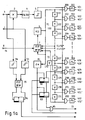
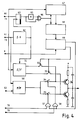
- the circuit arrangement according to FIG. 1 is supplied with a frequency-modulated intermediate frequency signal at 1, which is mixed in a mixing circuit with an IF carrier which is supplied at 3.
- a filter 4 connected to the mixing circuit 2
- the baseband which has a bandwidth of 150 kHz in VHF broadcasting is filtered out.
- This is fed to a limiter 5, at the output of which a rectangular signal is present, the frequency of which corresponds to the respective stroke of the frequency-modulated signal.
- clock pulses T1 are generated with the aid of a controllable oscillator (VCO) 6, which can be controlled by a frequency and phase comparator 7.
- VCO controllable oscillator
- the frequency and phase comparator 7 is supplied with a clock signal T4 at 8 with a reference frequency.
- the frequency of the clock pulses T1 emitted by the controllable oscillator 6 is 15.625 MHz.
- the clock pulses are passed over a runtime chain 100, which consists of 32 links 101 to 132. One link delays the clock pulses by 2 ns each.
- the clock T1 and the clock pulses which have passed through the entire delay chain 100 are fed to the frequency and phase comparator 7.
- the controllable oscillator 6 is controlled by comparing the delayed clock pulses T2 and the clock pulses T1 such that the period of the clock pulses T1 corresponds exactly to 32 times the delay of a link 101 to 132.
- the taps of the runtime chain 100 including its input and its output, thus have pulses which are each delayed by 2 ns to one another. These pulses are each fed to an input of one of the AND circuits 201 to 232.
- the output of the limiter 5 is supplied to the other inputs of the AND circuits 201 to 232.
- a pulse shaper 301 to 332 is connected to the outputs of the AND circuits 201 to 232. These each have two outputs, at which two time-shifted output pulses occur as a result of an input pulse. Since the clock pulses T1 are meandering, a pulse occurs alternately at the two outputs of each pulse shaper 301 to 332 at a distance of 32 ns - as long as the positive half-wave of the square-wave signal is present at the output of the limiter 5.
- the outputs of the pulse shapers 301 to 332 are denoted by 401 to 432 and 401 ⁇ to 432 ⁇ .
- the clock inputs of the counters are assigned to the outputs of pulse shapers 401 to 432 via OR circuits 51 to 58, which each have eight inputs A to H.
- the distribution of the count pulses 401 to 432 ⁇ takes place according to the scheme shown in Fig. 3 to the inputs A to H of the OR circuits 51 to 58.
- the division is made such that the count pulses at the inputs A to H of an OR gate always have the same distance and do not follow each other too closely, so that the clock limit frequency of the subsequent counter is not exceeded. Due to a larger number of OR circuits and counters, counters can also be used which are only suitable for lower clock frequencies.
- the output signal of the limiter 5 is then equal to 0 - the measured value is to be formed from all counter readings.
- a summation of all meter readings must take place in the shortest possible time.
- the counter readings are switched through in succession to an adder.
- the outputs of the flip-flops 71 to 79 are connected to output registers of the counters 61 to 68.
- the outputs of the meters are low-impedance when switched through and otherwise high-impedance.
- the clock signal T3 for the shift register 71 to 79 is obtained with the frequency divider 81 from the clock pulses T1. As soon as the limited frequency-modulated intermediate frequency signal has become 0, the flip-flop 82 is set. The flip-flop 83 is then also set with the next clock pulse T3 and the clock for the shift registers 71 to 79 is thus released via the AND circuit 85.
- the last flip-flop 79 of the shift register no longer switches through the counter reading to the adder 86, but ends the summation by resetting the shift register 71 to 79 to the value 1, the two flip-flops 82, 83 and the counters 61 to 68 resets and transfers the value of the sum memory 87 into an output memory 89.
- the measurement result is then available in digital form at the output 90 of the output memory.
- the sum memory 87 is also deleted. For this purpose, a corresponding signal is fed from the output of the flip-flop 79 via a delay circuit 91 to a reset input 92 of the sum memory 87.
- the values in the output memory are inversely proportional to the FM frequency swing and are converted into values that are proportional to the frequency by creating reciprocal values. Since the sign of this difference is also important when measuring the frequency swing, ie the instantaneous deviation of the frequency of the modulated signal from the associated carrier, a sign bit is derived, as described below.
- both the carrier and the frequency-modulated signal are each fed via a limiter 93, 94 to a further frequency and phase comparator 95, with the two output signals of which a flip-flop 96 is controlled, at whose output 97 the sign bit can be tapped.
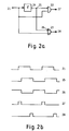
- FIG. 2a shows a block diagram of one of the pulse shapers and FIG. 2b shows diagrams of the signals occurring.
- the individual lines in FIG. 2b are provided with the same reference symbols as the circuit points in FIG. 2a at which the signals shown occur.
- the input 21 of the pulse shaper is connected to the output of one of the AND circuits 201 to 232 (FIG. 1a) and receives the meandering pulses shown in line 21 in FIG. 2b. These are each fed to an input of an AND circuit 22 and an OR circuit 23. In addition, they are delayed by a delay circuit 24 by a fraction of the period.
- the delayed meandering signals are shown in line 25 of FIG. 2b and are each fed to an inverting input of the AND circuit 22 and the NOR circuit 23.
- the inverted signal is shown in Fig. 2b, line 26.
- the AND operation of the signals according to line 21 and line 26 results in the pulses shown in line 27.
- the pulses shown in line 28 are created by NOR linking the same signals.
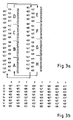
- the sequence in which the individual counting pulses occur is shown schematically in FIG. 3a.
- the counter pulses are compared to the inputs A to H of the OR circuits 51 to 58 shown in FIG. 1b.
- the counting impulses of the outputs 401 to 432 are contained in one cycle marked by arrows, while the inputs of the OR gates are shown in a second cycle which is run through with the same frequency.
- the table shown in FIG. 3b shows once again the assignment of the outputs of the pulse shapers 301 to 332 to the inputs of the OR circuits 51 to 58.
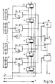
- Fig. 4 shows a block diagram of the frequency and phase comparator 7 (Fig. 1a).
- the desired frequency is first set (after switching on) with a frequency comparator .
- the phase at the input and output of the runtime chain is then regulated to 0 ° or 360 ° using a fast phase comparator. It is continuously checked whether the controllable oscillator has to be controlled with the frequency comparator or with the phase comparator.
- the signal T1 generated by the controllable oscillator 6 is fed via the input 41 to the circuit according to FIG. 2 and reaches a frequency divider 42.
- the output signal of the frequency divider 42 is mixed in a D flip-flop 43 with a reference signal T4 supplied at 44.
- a signal with the difference frequency is available at the output of the D flip-flop 43.
- a short pulse is derived from each positive and negative edge of this signal with the aid of the delay circuit 45 and the EXCL-OR circuit 46, which takes over the counter reading of a counter 47 into a memory 48 and then resets the counter 47.
- the counter 48 counts the clocks of the reference signal T4 in each case between adjacent pulses at the output of the EXCL-OR gate 46.
- the counter 48 counts up to an upper limit value, which prevents an overflow.
- the content of the memory 48 is compared with a predetermined value K in a comparator 49. If the content of the memory 48 is less than the value K, then the frequency comparator 31 is switched on, the switches 32 and 33 then being conductive, while the switches 34 and 35 being non-conductive. Otherwise, the phase comparator 50 is used.
- phase comparator 50 the output signal of which, if the phase position coincides, is 0 V and if there are deviations between the clock signals T1 and T2, positive or negative.
- the control voltage is fed to the controllable oscillator 6 (FIG. 1a) via an output stage 36.
- the runtime chain 100 contains taps in which the phase rotation of the signal T1 is 90 ° or 270 ° when the target frequency is present.
- These signals T1 / 90 ° and T1 / 270 ° determine after AND operations with the output signal of the phase comparator 50 (FIG. 4) in the circuit arrangement according to FIG. 4 via the AND gates 37 and 38, when the switches 34 and 35 are closed are provided that a corresponding signal is fed from the comparator 49 to the other inputs of the AND circuits 37 and 38, which means that the frequencies of the signals T1 and T4 differ only slightly from one another.
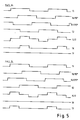
- signals appearing in the circuit arrangement are shown in FIG. 5. They are given the same name as those points of the circuit arrangement at which they occur. The signals are shown for two cases. In case A, the total delay of the runtime chain is small and in case B, the total delay is too large.
- the signal T1 / 2 is the output signal of a differential amplifier, which works as a phase comparator 50 (FIG. 4).
- the output voltage is negative if T1 is less than T2, zero if T1 is T2, and positive if T1 is greater than T2.
- the signal T1 / 2 is now AND-linked with the signals T1 / 90 ° and T1 / 270 °, the negative values of T1 / 2 being set to zero.
- the signals T1 / 2 + T1 / 90 ° abbreviated TX and T1 / 2 + T1 / 270 ° abbreviated TY arise, with which the gates 37 and 38 (FIG. 4) are controlled will.
Abstract
Description
Die Erfindung geht aus von einem Verfahren nach der Gattung des Anspruchs 1.The invention is based on a method according to the preamble of
Es ist schon ein Verfahren zur Messung der Frequenz eines Signals bekannt, bei welchem Perioden des Signals über einen vorgegebenen Zeitabschnitt gezählt werden und das Ergebnis auf eine Sekunde umgerechnet wird. Dieses Verfahren kann jedoch nicht bei Signalen angewendet werden, deren Frequenz sich laufend ändert, es sei denn, man möchte die mittlere Frequenz messen.A method for measuring the frequency of a signal is already known, in which periods of the signal are counted over a predetermined period of time and the result is converted to a second. However, this method cannot be used for signals whose frequency is constantly changing unless you want to measure the average frequency.
Aus der DE-A-27 35 785 ist es zur Messung des arithmetischen Mittelwertes der Frequenz eines Signals bekannt, Triggerimpulse aus dem Signalverlauf abzuleiten und diese in einem Schieberegister zu speichern. Die Anzahl der besetzten Registerzellen erlaubt eine Aussage über die mittlere Frequenz im Verhältnis zu der Taktfrequenz, mit der die Triggerimpulse durch das Schieberegister hindurchgeschoben werden. Die zu messende Frequenz kann hierbei den Wert der Taktfrequenz erreichen.From DE-A-27 35 785 it is known for measuring the arithmetic mean of the frequency of a signal to derive trigger pulses from the signal curve and to store them in a shift register. The number of occupied register cells allows a statement about the average frequency in relation to the clock frequency with which the trigger pulses are pushed through the shift register. The frequency to be measured can reach the value of the clock frequency.
Es sind jedoch auch Verfahren bekannt geworden, bei denen durch Zählung von Impulsen die Periodendauer des Signals bestimmt wird. Um eine genügend hohe Auflösung des Ergebnisses zu erhalten, benötigt man hierfür Zählimpulse, deren Frequenz wesentlich höher als die zu messende Frequenz ist. Insbesondere bei der hochauflösenden Messung von frequenzmodulierten Zwischenfrequenzsignalen ergeben sich für die bekannten Verfahren Werte, welche sich nicht mit bekannten Bauelementen realisieren lassen. Wollte man beispielsweise ein derartiges Signal in der Zwischenfrequenzebene (10,7 MHz) mit einer Genauigkeit von 12 Bit erfassen, müßte man für die letzte Stelle eine Periodendauerdifferenz von 0,32 ps erfassen können. Ein Meßverfahren, das diese Genauigkeit erreicht, ist nicht realisierbar. Bei der geforderten Genauigkeit erreicht man auch bei einer Herabsetzung des Zwischenfrequenzsignals in das Basisband keine realisierbaren Werte. Als Zählfrequenz wären dazu mindestens 614,4 MHz erforderlich. Dieses kann ebenfalls aus den verschiedensten Gründen nicht verwirklicht werden.However, methods have also become known in which the period of the signal is determined by counting pulses. In order to obtain a sufficiently high resolution of the result, one needs counting pulses whose frequency is significantly higher than the frequency to be measured. Especially for high-resolution measurement of frequency-modulated Intermediate frequency signals result in values for the known methods which cannot be realized with known components. For example, if you wanted to detect such a signal in the intermediate frequency level (10.7 MHz) with an accuracy of 12 bits, you would have to be able to detect a period difference of 0.32 ps for the last digit. A measuring method that achieves this accuracy cannot be implemented. With the required accuracy, even if the intermediate frequency signal is reduced to the baseband, no realizable values are achieved. At least 614.4 MHz would be required as the counting frequency. This can also not be realized for a variety of reasons.
Das erfindungsgemäße Verfahren mit den kennzeichnenden Merkmalen des Anspruchs 1 hat demgegenüber den Vorteil, daß eine Frequenzmessung des Zwischenfrequenzsignals mit extrem hoher Auflösung unter Benutzung verfügbarer elektronischer Bauelemente möglich ist. Das erfindungsgemäße Verfahren ist nicht auf die Messung von Zwischenfrequenzsignalen beschränkt, sondern kann im Rahmen des Fachmännischen auch für andere Signale verwendet werden. Es hat zudem den Vorteil, daß der Meßwert digital als Ausgangswert zur Verfügung steht und so eine digitale Weiterverarbeitung des Signals erlaubt.The inventive method with the characterizing features of
Durch die in den Unteransprüchen aufgeführten Maßnahmen sind vorteilhafte Weiterbildungen und Verbesserungen des erfindungsgemäßen Verfahrens möglich. Schaltungsanordnungen zur Durchführung des erfindungsgemäßen Verfahrens sind in den Ansprüchen 4 bis 9 aufgeführt.Advantageous further developments and improvements of the method according to the invention are possible through the measures listed in the subclaims. Circuit arrangements for performing the method according to the invention are listed in
Ein Ausführungsbeispiel der Erfindung ist in der Zeichnung an Hand mehrerer Figuren dargestellt und in der nachfolgenden Beschreibung näher erläutert.
Es zeigt:
- Fig. 1
- ein Blockschaltbild einer Schaltungsanordnung zur Durchführung des erfindungsgemäßen Verfahrens, welches wegen seines Umfangs auf Figuren 1a und 1b verteilt ist,
- Fig. 2
- ein Blockschaltbild eines in der Schaltungsanordnung nach Fig. 1 verwendeten Impulsformers,
- Fig. 3
- schematische Darstellungen zur Zuordnung der Ausgänge der Impulsformer zu Eingängen von ODER-Schaltungen innerhalb der Schaltungsanordnung nach Fig. 1,
- Fig. 4
- ein Blockschaltbild eines bei der Schaltungsanordnung nach Fig. 1 verwendeten Frequenz-und Phasenkomparators und
- Fig. 5
- Diagramme der bei dem Frequenz- und Phasenkomparators nach Fig. 4 auftretenden Signale.
It shows:
- Fig. 1
- 2 shows a block diagram of a circuit arrangement for carrying out the method according to the invention, which is distributed over FIGS. 1a and 1b because of its scope,
- Fig. 2
- 2 shows a block diagram of a pulse shaper used in the circuit arrangement according to FIG. 1,
- Fig. 3
- 1 shows schematic representations for assigning the outputs of the pulse shapers to inputs of OR circuits within the circuit arrangement according to FIG. 1,
- Fig. 4
- 2 shows a block diagram of a frequency and phase comparator used in the circuit arrangement according to FIG. 1 and
- Fig. 5
- Diagrams of the signals occurring in the frequency and phase comparator according to FIG. 4.
Gleiche Teile sind in den Figuren mit gleichen Bezugszeichen versehen.Identical parts are provided with the same reference symbols in the figures.
Der Schaltungsanordnung nach Fig. 1 wird bei 1 ein frequenzmoduliertes Zwischenfrequenzsignal zugeführt, welches in einer Mischschaltung mit einem ZF-Träger, der bei 3 zugeführt wird, gemischt wird. Mit Hilfe eines an die Mischschaltung 2 angeschlossenen Filters 4 wird aus dem Mischprodukt das Basisband, welches beim UKW-Rundfunk eine Bandbreite von 150 kHz hat, herausgefiltert. Dieses wird einem Begrenzer 5 zugeleitet, an dessen Ausgang ein rechteckförmiges Signal anliegt, dessen Frequenz dem jeweiligen Hub des frequenzmodulierten Signals entspricht.The circuit arrangement according to FIG. 1 is supplied with a frequency-modulated intermediate frequency signal at 1, which is mixed in a mixing circuit with an IF carrier which is supplied at 3. With the help of a
Die Erzeugung von Taktimpulsen T1 erfolgt bei der Schaltungsanordnung nach Fig. 1 mit Hilfe eines steuerbaren Oszillators (VCO) 6, der von einem Frequenz- und Phasenkomparator 7 steuerbar ist. Dem Frequenz- und Phasenkomparator 7 wird bei 8 ein Taktsignal T4 mit einer Referenzfrequenz zugeführt. Die Frequenz der vom steuerbaren Oszillator 6 abgegebenen Taktimpulse T1 beträgt 15,625 MHz. Die Taktimpulse werden über eine Laufzeitkette 100 geleitet, welche aus 32 Gliedern 101 bis 132 besteht. Ein Glied verzögert die Taktimpulse um jeweils 2 ns. Der Takt T1 und die Taktimpulse, welche die gesamte Verzögerungskette 100 durchlaufen haben, werden dem Frequenz- und Phasenkomparator 7 zugeführt.In the circuit arrangement according to FIG. 1, clock pulses T1 are generated with the aid of a controllable oscillator (VCO) 6, which can be controlled by a frequency and
In später genauer beschriebener Weise wird durch Vergleich der verzögerten Taktimpulse T2 und der Taktimpulse T1 der steuerbare Oszillator 6 derart gesteuert, daß die Periodendauer der Taktimpulse T1 genau dem 32-fachen der Verzögerung eines Gliedes 101 bis 132 entspricht. An den Anzapfungen der Laufzeitkette 100 einschließlich deren Eingang und deren Ausgang stehen somit Impulse an, welche jeweils um 2 ns zueinander verzögert sind. Diese Impulse werden je einem Eingang einer der UND-Schaltungen 201 bis 232 zugeführt.In a manner described in more detail later, the
Den anderen Eingängen der UND-Schaltungen 201 bis 232 wird das Ausgangssignal des Begrenzers 5 zugeführt. An die Ausgänge der UND-Schaltungen 201 bis 232 ist je ein Impulsformer 301 bis 332 angeschlossen. Diese weisen jeweils zwei Ausgänge auf, an denen als Folge eines Eingangsimpulses zwei zeitlich versetzte Ausgangsimpulse auftreten. Da die Taktimpulse T1 mäanderförmig sind, tritt somit abwechselnd an den beiden Ausgängen jedes Impulsformers 301 bis 332 im Abstand von 32 ns ein Impuls auf - und zwar solange, wie am Ausgang des Begrenzers 5 die positive Halbwelle des Rechtecksignals ansteht. In den Figuren 1 und 3 sind die Ausgänge der Impulsformer 301 bis 332 mit 401 bis 432 sowie 401ʹ bis 432ʹ bezeichnet.The output of the
Wegen der hohen Frequenz aller Ausgangsimpulse der Impulsformer 301 bis 332 zusammengenommen werden zur Zählung der gesamten Anzahl der Impulse acht Zähler 61 bis 68 benötigt. Dabei erfolgt die Zuordnung der Takteingänge der Zähler zu den Ausgängen der Impulsformer 401 bis 432 über ODER-Schaltungen 51 bis 58, welche jeweils acht Eingänge A bis H aufweisen. Die Verteilung der Zählimpulse 401 bis 432ʹ erfolgt nach dem in Fig. 3 dargestellten Schema auf die Eingänge A bis H der ODER-Schaltungen 51 bis 58. Die Aufteilung ist derart vorgenommen, daß die Zählimpulse an den Eingängen A bis H eines ODER-Gatters zeitlich immer den gleichen Abstand haben und nicht zu dicht aufeinander folgen, so daß die Taktgrenzfrequenz des nachfolgenden Zählers nicht überschritten wird. Durch eine größere Zahl von ODER-Schaltungen und Zählern können auch Zähler verwendet werden, welche nur für geringere Taktfrequenzen geeignet sind.Because of the high frequency of all output pulses of
Nachdem die Periodendauerzählung beendet ist - das Ausgangssignal des Begrenzers 5 ist dann gleich 0 -, ist der Meßwert aus allen Zählerständen zu bilden. Dazu hat in möglichst kurzer Zeit eine Summenbildung aller Zählerstände zu erfolgen. Mittels eines Schieberegisters, das aus den Flip-Flops 71 bis 79 besteht und zu Beginn der Aufsummierung auf den Wert 1 gesetzt wurde, werden nacheinander die Zählerstände zu einem Addierer durchgeschaltet. Dazu sind die Ausgänge der Flip-Flops 71 bis 79 mit Ausgangsregistern der Zähler 61 bis 68 verbunden. Die Ausgänge der Zähler sind im durchgeschalteten Zustand niederohmig und anderenfalls hochohmig.After the period counting has ended - the output signal of the
Das Taktsignal T3 für das Schieberegister 71 bis 79 wird mit dem Frequenzteiler 81 aus den Taktimpulsen T1 gewonnen. Sobald das begrenzte frequenzmodulierte Zwischenfrequenzsignal 0 geworden ist, wird das Flip-Flop 82 gesetzt. Danach wird mit dem nächsten Taktimpuls T3 auch das Flip-Flop 83 gesetzt und damit der Takt für das Schieberegister 71 bis 79 über die UND-Schaltung 85 freigegeben.The clock signal T3 for the
Mit der positiven Flanke des Schiebetaktes T3 wird der jeweilige Zählerstand zum Addierer 86 durchgeschaltet und mit jeder negativen Flanke des Schiebetaktes das Ergebnis des Addierers 86 in einen Summenspeicher 87 übernommen, wozu das Taktsignal T3 den Steuereingang 88 eines Eingangsregisters des Summenspeichers 87 zugeführt wird. Das so in dem Summenspeicher 87 festgehaltene Zwischenergebnis wird bei der nächsten Addition wieder als ein Summand verwendet.With the positive edge of the shift clock T3, the respective counter reading is switched through to the adder 86 and with each negative edge of the shift clock the result of the adder 86 is transferred to a sum memory 87, for which purpose the clock signal T3 is fed to the control input 88 of an input register of the sum memory 87. The intermediate result thus retained in the sum memory 87 is used again as a summand in the next addition.
Das letzte Flip-Flop 79 des Schieberegisters schaltet keinen Zählerstand zum Addierer 86 mehr durch, sondern beendet die Summenbildung, indem es das Schieberegister 71 bis 79 wieder auf den Wert 1 setzt, die beiden Flip-Flops 82, 83 sowie die Zähler 61 bis 68 rücksetzt und den Wert des Summenspeichers 87 in einen Ausgabespeicher 89 überträgt. Am Ausgang 90 des Ausgabespeichers steht dann das Meßergebnis in digitaler Form zur Verfügung.The last flip-
Nach erfolgter Übertragung des Meßergebnisses aus dem Summenspeicher 87 in den Ausgabespeicher 89 wird der Summenspeicher 87 ebenfalls gelöscht. Hierzu wird vom Ausgang des Flip-Flops 79 über eine Verzögerungsschaltung 91 einem Rücksetzeingang 92 des Summenspeichers 87 ein entsprechendes Signal zugeführt.After the measurement result has been transferred from the sum memory 87 to the
Die Werte im Ausgabespeicher sind dem FM-Frequenzhub umgekehrt proportional und werden durch Kehrwertbildung in Werte umgerechnet, welche der Frequenz proportional sind. Da bei der Messung des Frequenzhubs, also der momentanen Abweichung der Frequenz des modulierten Signals vom zugehörigen Träger auch das Vorzeichen dieser Differenz von Bedeutung ist, wird - wie im folgenden beschrieben - ein Vorzeichenbit abgeleitet. Dazu wird sowohl der Träger als auch das frequenzmodulierte Signal über je einen Begrenzer 93, 94 einem weiteren Frequenz- und Phasenkomparator 95 zugeführt, mit dessen beiden Ausgangssignalen ein Flip-Flop 96 gesteuert wird, an dessen Ausgang 97 das Vorzeichenbit abgreifbar ist.The values in the output memory are inversely proportional to the FM frequency swing and are converted into values that are proportional to the frequency by creating reciprocal values. Since the sign of this difference is also important when measuring the frequency swing, ie the instantaneous deviation of the frequency of the modulated signal from the associated carrier, a sign bit is derived, as described below. For this purpose, both the carrier and the frequency-modulated signal are each fed via a
Im folgenden werden an Hand von Fig. 2 die Impulsformer 301 bis 332 erläutert. Dabei stellen Fig. 2a ein Blockschaltbild eines der Impulsformer und Fig. 2b Diagramme der auftretenden Signale dar. Die einzelnen Zeilen in Fig. 2b sind mit den gleichen Bezugszeichen versehen wie die Schaltungspunkte in Fig. 2a, an welchen die dargestellten Signale auftreten.The pulse shapers 301 to 332 are explained below with reference to FIG. 2. 2a shows a block diagram of one of the pulse shapers and FIG. 2b shows diagrams of the signals occurring. The individual lines in FIG. 2b are provided with the same reference symbols as the circuit points in FIG. 2a at which the signals shown occur.
Der Eingang 21 des Impulsformers ist an den Ausgang einer der UND-Schaltungen 201 bis 232 (Fig. 1a) angeschlossen und empfängt die in Fig. 2b in Zeile 21 dargestellten mäanderförmige Impulse. Diese werden je einem Eingang einer UND-Schaltung 22 und einer ODER-Schaltung 23 zugeführt. Außerdem werden sie von einer Verzögerungsschaltung 24 um einen Bruchteil der Periodendauer verzögert.The
Die verzögerten mäanderförmigen Signale sind in Zeile 25 der Fig. 2b dargestellt und werden jeweils einem invertierenden Eingang der UND-Schaltung 22 und der NOR-Schaltung 23 zugeleitet. Das invertierte Signal ist in Fig. 2b, Zeile 26 gezeigt. Durch die UND-Verknüpfung der Signale nach Zeile 21 und Zeile 26 ergeben sich die in Zeile 27 gezeigten Impulse. Durch die NOR-Verknüpfung der gleichen Signale entstehen die in Zeile 28 gezeigten Impulse.The delayed meandering signals are shown in
Durch die Aufteilung der Ausgangsimpulse der UND-Schaltungen 201 bis 232 (Fig. 1a) in jeweils zwei zeitlich um eine halbe Periodendauer gegeneinander versetzte Impulse wird eine Verdopplung der Anzahl der Zählimpulse und damit eine Verdopplung der Genauigkeit erzielt. Dieses setzt jedoch eine geeignete Verschachtelung aller von den Impulsformern 301 bis 332 abgegebenen Impulse voraus. Dabei ist zu berücksichtigen, daß die Zeitverzögerung von einer Anzapfung der Laufzeitkette 100 zur nächsten nur 2 ns beträgt, daß sich jedoch die Zeitdifferenz zwischen den Impulsen an den oberen Ausgängen der Impulsformer und den Impulsen an den unteren Ausgängen auf 32 ns beläuft.By dividing the output pulses of the AND
Die Reihenfolge des Auftretens der einzelnen Zählimpulse ist in Fig. 3a schematisch dargestellt. Zusätzlich sind den Zählimpulsen die Eingänge A bis H der in Fig. 1b dargestellten ODER-Schaltungen 51 bis 58 gegenübergestellt. In einem durch Pfeile markierten Umlauf sind die Zählimpulse der Ausgänge 401 bis 432 enthalten, während in einem zweiten Umlauf, der mit gleicher Frequenz durchlaufen wird, die Eingänge der ODER-Gatter dargestellt sind.The sequence in which the individual counting pulses occur is shown schematically in FIG. 3a. In addition, the counter pulses are compared to the inputs A to H of the
Die in Fig. 3b wiedergegebene Tabelle zeigt noch einmal die Zuordnung der Ausgänge der Impulsformer 301 bis 332 zu den Eingängen der ODER-Schaltungen 51 bis 58.The table shown in FIG. 3b shows once again the assignment of the outputs of the
Fig. 4 zeigt ein Blockschaltbild des Frequenz- und Phasenkomparators 7 (Fig. 1a). Um zu erreichen, daß der steuerbare Oszillator 6 (Fig. 1) auf einer Frequenz schwingt, bei welcher der Ausgangstakt T1 mit der gesamten Laufzeitkette 100 genau um eine Periodendauer verzögert wird, wird zunächst (nach dem Einschalten) mit einem Frequenzkomparator die gewünschte Frequenz eingestellt. Anschließend wird mit einem schnellen Phasenkomparator die Phase am Eingang und am Ausgang der Laufzeitkette auf 0° bzw. 360° geregelt. Dabei wird laufend geprüft, ob die Regelung des steuerbaren Oszillators mit dem Frequenzkomparator oder mit dem Phasenkomparator zu erfolgen hat.Fig. 4 shows a block diagram of the frequency and phase comparator 7 (Fig. 1a). In order to ensure that the controllable oscillator 6 (FIG. 1) oscillates at a frequency at which the output clock T1 with the
Dazu wird das vom steuerbaren Oszillator 6 erzeugte Signal T1 über den Eingang 41 der Schaltung nach Fig. 2 zugeführt und gelangt in einen Frequenzteiler 42.For this purpose, the signal T1 generated by the
Das Ausgangssignal des Frequenzteilers 42 wird in einem D-Flip-Flop 43 mit einem bei 44 zugeführten Referenzsignal T4 gemischt. Am Ausgang des D-Flip-Flops 43 steht ein Signal mit der Differenzfrequenz zur Verfügung. Aus jeder positiven und negativen Flanke dieses Signals wird mit Hilfe der Verzögerungsschaltung 45 und der EXCL-ODER-Schaltung 46 ein kurzer Impuls abgeleitet, der den Zählerstand eines Zählers 47 in einen Speicher 48 übernimmt und den Zähler 47 anschließend rücksetzt. Der Zähler 48 zählt die Takte des Referenzsignals T4 jeweils zwischen benachbarten Impulsen am Ausgang des EXCL-ODER-Gatters 46. Der Zähler 48 zählt bis zu einem oberen Grenzwert, womit ein Überlauf verhindert wird. In einem Komparator 49 wird der Inhalt des Speichers 48 mit einem vorgegebenen Wert K verglichen. Wenn der Inhalt des Speichers 48 kleiner ist als der Wert K, dann wird der Frequenzkomparator 31 eingeschaltet, wobei die Schalter 32 und 33 dann leitend sind, während die Schalter 34 und 35 nichtleitend sind. Ansonsten wird der Phasenkomparator 50 benutzt.The output signal of the
Weil die Phasenregelung sehr schnell und genau sein muß, wird ein Differenzverstärker als Phasenkomparator 50 verwendet, dessen Ausgangssignal bei übereinstimmender Phasenlage 0 V und bei Abweichungen zwischen den Taktsignalen T1 und T2 positiv oder negativ ist. Über eine Ausgangsstufe 36 wird die Steuerspannung dem steuerbaren Oszillator 6 (Fig. 1a) zugeleitet.Because the phase control must be very fast and precise, a differential amplifier is used as the
Die Laufzeitkette 100 enthält Anzapfungen, bei denen die Phasendrehung des Signals T1 bei Vorliegen der Sollfrequenz 90° bzw. 270° beträgt. Diese Signale T1/90° und T1/270° bestimmen nach UND-Verknüpfungen mit dem Ausgangssignal des Phasenkomparators 50 (Fig. 4) bei der Schaltungsanordnung nach Fig. 4 über die UND-Gatter 37 und 38, wann die Schalter 34 und 35 geschlossen werden, unter der Voraussetzung, daß vom Komparator 49 ein entsprechendes Signal den anderen Eingängen der UND-Schaltungen 37 und 38 zugeführt wird, welches besagt, daß die Frequenzen der Signale T1 und T4 nur geringfügig voneinander abweichen.The
Zur weiteren Erläuterung der Schaltungsanordnung nach Fig. 4 sind in Fig. 5 Signale, welche in der Schaltungsanordnung auftreten, dargestellt. Sie sind gleichlautend mit denjenigen Punkten der Schaltungsanordnung bezeichnet, an welchen sie auftreten. Die Signale sind für zwei Fälle dargestellt. Im Fall A ist nämlich die Gesamtverzögerung der Laufzeitkette zugering und im Fall B ist die Gesamtverzögerung zu groß.For further explanation of the circuit arrangement according to FIG. 4, signals appearing in the circuit arrangement are shown in FIG. 5. They are given the same name as those points of the circuit arrangement at which they occur. The signals are shown for two cases. In case A, the total delay of the runtime chain is small and in case B, the total delay is too large.
Das Signal T1/2 ist das Ausgangssignal eines Differenzverstärkers, der als Phasenkomparator 50 (Fig. 4) arbeitet. Die Ausgangsspannung ist negativ, wenn T1 kleiner als T2 ist, Null, wenn T1 gleich T2 ist, und positiv, wenn T1 größer als T2 ist. Das Signal T1/2 wird nun mit den Signalen T1/90° und T1/270° UND-verknüpft, wobei die negativen Werte von T1/2 zu Null gesetzt werden. Es entstehen die Signale T1/2 + T1/90° abgekürzt TX und T1/2 + T1/270° abgekürzt TY, mit denen die Gatter 37 und 38 (Fig. 4) angesteuert werden.The signal T1 / 2 is the output signal of a differential amplifier, which works as a phase comparator 50 (FIG. 4). The output voltage is negative if T1 is less than T2, zero if T1 is T2, and positive if T1 is greater than T2. The signal T1 / 2 is now AND-linked with the signals T1 / 90 ° and T1 / 270 °, the negative values of T1 / 2 being set to zero. The signals T1 / 2 + T1 / 90 ° abbreviated TX and T1 / 2 + T1 / 270 ° abbreviated TY arise, with which the
Claims (9)
- Method of measuring the frequency of a signal, in which counting pulses derived from clock pulses are counted and the counting result is output as a digital signal, characterised in that the frequency of the counting pulses corresponds to a multiple of the frequency of the clock pulses, in that the counting pulses occur at various tapping points of a delay line (101 - 132), in that the signal is limited in a limiter (5) in such a way that, during a half-wave of the signal, the output signal of the limiter (5) is greater than zero, in that the counting pulses are counted during a half-wave with the aid of a plurality of counters (61 - 68) and in that, after expiry of this half-wave of the signal, the contents of the counters (61 - 68) are combined and converted by means of reciprocal-value formation into the corresponding frequency information.
- Method according to Claim 1, characterised in that, for measuring the frequency of a frequency-modulated signal, the latter is mixed with an associated carrier in a mixer (2).
- Method according to Claim 2, characterised in that an operational-sign signal is obtained by frequency and phase comparison in a comparator (95) of the frequency-modulated signal which has been amplitudelimited in a second limiter (93) with a carrier which has been amplitude-limited in a third limiter (94).
- Circuit arrangement for carrying out the method according to Claim 1, characterised in that the output of an oscillator (6) provided for generating the clock pulses is connected to the input of the delay line (100), in that the delay line (100) has n elements (101 - 132), n corresponding to the ratio between the frequencies of the counting pulses and the clock pulses, in that the input of the delay line (100) as well as the tapping points lying between the elements (101 - 132) are connected to a first input each of an AND circuit (201 - 232), in that a square-wave voltage which has the frequency of the signal to be measured is applied to second inputs of the AND circuits (201 - 232), and in that the outputs of the AND circuits (201 - 232) are connected via OR circuits (51 - 58) to inputs of counters (61 - 68), the outputs of which are connected to an adding and storing circuit (86, 87, 89).
- Circuit arrangement according to Claim 4, characterised in that pulse shapers (301 - 332) are connected in each case between the outputs of the AND circuits (201 - 232) and inputs of the OR circuits (51 - 58) and emit at a first output (401 - 432) pulses triggered by the leading edges of the fed pulses and at a second output (401' - 432') pulses triggered by the trailing edges.
- Circuit arrangement according to Claim 4, characterised in that the frequency of the oscillator (6) can be controlled with the aid of a frequency comparator (31) and a phase comparator (50), in that the frequency comparator (31) is fed the clock pulses and a signal having a reference frequency, in that the phase comparator (50) is fed the clock pulses respectively from the output of the oscillator (6) and from the output of the delay line (100) and in that a switching-over device (32-35, 42-49) is provided, which switches over from the frequency comparator (31) to the phase comparator (50), dependent on whether the difference between the reference frequency and the clock frequency drops below a predetermined value.
- Circuit arrangement according to Claim 4, characterised in that outputs of the counters (61 - 68) are connected via a cyclical change-over switch to the adding and storing circuit (86, 87, 89), in that the change-over switch can be fed switching pulses from a frequency divider (81) via a gate circuit (82 - 85), the input of the frequency divider (81) being connected to the output of the oscillator (6), and in that the gate circuit (82 - 85) can be controlled in such a way that, after expiry of a counting-out time period, switching pulses are fed to the change-over switch and in that the feeding of the switching pulses does not take place if the change-over switch has completed a switching cycle.
- Circuit arrangement according to Claim 7, characterised in that the change-over switch is formed by a shift register (71 - 79) and output registers of the counters (61 - 68), in that the switching pulses are fed to the shift register as a clock and in that an output of one of the flip-flops forming the shift register (71 - 79) is connected to recessing inputs of the counters of the shift register and to a control input of the gate circuit (82, 83, 85).
- Circuit arrangement according to Claim 4, characterised in that the adding and storing circuit (86, 87, 89) is formed by an adder (86), a sum memory (87) and an output memory (89), in that one input of the adder (86) is connected via a change-over switch to the outputs of the counters (61 - 68) and the other input of the adder (86) is connected to an output of the sum memory (87), in that an input of the sum memory (87) is connected to the output of the adder (86) and in that the output of the sum memory (87) is connected to an input of the output memory (89).
Priority Applications (1)
| Application Number | Priority Date | Filing Date | Title |
|---|---|---|---|
| AT87105445T ATE80952T1 (en) | 1986-04-26 | 1987-04-13 | METHOD AND ARRANGEMENT FOR RAPID AND ACCURATE MEASUREMENT OF THE FREQUENCY OF A SIGNAL. |
Applications Claiming Priority (2)
| Application Number | Priority Date | Filing Date | Title |
|---|---|---|---|
| DE3614272 | 1986-04-26 | ||
| DE19863614272 DE3614272A1 (en) | 1986-04-26 | 1986-04-26 | METHOD AND ARRANGEMENT FOR FAST AND PRECISE MEASUREMENT OF THE FREQUENCY OF A SIGNAL |
Publications (3)
| Publication Number | Publication Date |
|---|---|
| EP0243771A2 EP0243771A2 (en) | 1987-11-04 |
| EP0243771A3 EP0243771A3 (en) | 1989-04-12 |
| EP0243771B1 true EP0243771B1 (en) | 1992-09-23 |
Family
ID=6299662
Family Applications (1)
| Application Number | Title | Priority Date | Filing Date |
|---|---|---|---|
| EP87105445A Expired - Lifetime EP0243771B1 (en) | 1986-04-26 | 1987-04-13 | Method and arrangement for the quick and precise measurement of the frequency of a signal |
Country Status (6)
| Country | Link |
|---|---|
| US (1) | US4745356A (en) |
| EP (1) | EP0243771B1 (en) |
| JP (1) | JPS62261073A (en) |
| AT (1) | ATE80952T1 (en) |
| DE (2) | DE3614272A1 (en) |
| ES (1) | ES2034976T3 (en) |
Families Citing this family (6)
| Publication number | Priority date | Publication date | Assignee | Title |
|---|---|---|---|---|
| US4786861A (en) * | 1987-09-01 | 1988-11-22 | Sundstrand Data Control, Inc. | Frequency counting apparatus and method |
| DE3736124A1 (en) * | 1987-10-26 | 1989-05-03 | Licentia Gmbh | METHOD AND ARRANGEMENT FOR DETERMINING THE TORQUE FREQUENCY OF A SIGNAL |
| DE3900292A1 (en) * | 1989-01-07 | 1990-07-12 | Acer Inc | FREQUENCY DETECTOR |
| US5610978A (en) * | 1994-12-30 | 1997-03-11 | Mitel Corporation | Ring discriminator |
| JP3691310B2 (en) * | 1999-10-21 | 2005-09-07 | 富士通株式会社 | Frequency measurement circuit |
| JP2021032761A (en) * | 2019-08-27 | 2021-03-01 | セイコーエプソン株式会社 | Frequency measurement circuit and frequency measuring device |
Family Cites Families (5)
| Publication number | Priority date | Publication date | Assignee | Title |
|---|---|---|---|---|
| US3086172A (en) * | 1959-12-18 | 1963-04-16 | Gen Electric | Tunable filter arrangement |
| JPS526189B2 (en) * | 1972-08-23 | 1977-02-19 | ||
| US4443766A (en) * | 1976-06-15 | 1984-04-17 | The United States Of America As Represented By The Secretary Of The Air Force | Precision digital sampler |
| DE2735785A1 (en) * | 1977-08-09 | 1979-02-22 | Bosch Gmbh Robert | Frequency measurement using digital switching - involves shift register whose stages deliver criterion proportional to frequency to be measured |
| US4270209A (en) * | 1979-12-07 | 1981-05-26 | International Telephone And Telegraph Corporation | Digital compressive receiver |
-
1986
- 1986-04-26 DE DE19863614272 patent/DE3614272A1/en not_active Withdrawn
-
1987
- 1987-04-13 EP EP87105445A patent/EP0243771B1/en not_active Expired - Lifetime
- 1987-04-13 ES ES198787105445T patent/ES2034976T3/en not_active Expired - Lifetime
- 1987-04-13 AT AT87105445T patent/ATE80952T1/en not_active IP Right Cessation
- 1987-04-13 DE DE8787105445T patent/DE3781825D1/en not_active Expired - Fee Related
- 1987-04-17 US US07/039,677 patent/US4745356A/en not_active Expired - Fee Related
- 1987-04-27 JP JP62102161A patent/JPS62261073A/en active Pending
Also Published As
| Publication number | Publication date |
|---|---|
| DE3781825D1 (en) | 1992-10-29 |
| ES2034976T3 (en) | 1993-04-16 |
| US4745356A (en) | 1988-05-17 |
| EP0243771A3 (en) | 1989-04-12 |
| EP0243771A2 (en) | 1987-11-04 |
| JPS62261073A (en) | 1987-11-13 |
| DE3614272A1 (en) | 1987-10-29 |
| ATE80952T1 (en) | 1992-10-15 |
Similar Documents
| Publication | Publication Date | Title |
|---|---|---|
| EP0043407B1 (en) | Arrangement for the digital measuring of phase difference | |
| DE2220878B2 (en) | Circuit arrangement for digital frequency measurement | |
| DE3234575A1 (en) | Method and arrangement for measuring frequencies | |
| EP0243771B1 (en) | Method and arrangement for the quick and precise measurement of the frequency of a signal | |
| DE2225462A1 (en) | Method and device for averaging the signals from a forward-backward signal generator | |
| EP0062698B1 (en) | Evaluation circuit for a digital rotational speed transducer | |
| DE2064513A1 (en) | Self-calibrating analog-to-digital converter that works according to the pulse rate method | |
| DE3023699A1 (en) | METHOD AND ARRANGEMENT FOR GENERATING IMPULSES AT PRESET TIME RELATION WITHIN PRESET IMPULSE INTERVALS WITH HIGH TIME RESOLUTION | |
| DE3714901C2 (en) | ||
| DE3836811C2 (en) | ||
| DE3843261A1 (en) | Circuit arrangement for controlling the phase of a clock signal | |
| DE1925917C3 (en) | Binary pulse frequency multiplier circuit | |
| DE2719147A1 (en) | Programmable pulse divider system - compares stored denominator with counter output to produce output pulses | |
| DE2002583C2 (en) | Circuit for counting up / down the interference fringes supplied by an optical system | |
| DE2522441C2 (en) | Monitoring system for electronic assemblies or devices in wired telecommunications systems | |
| DE2343472C3 (en) | Circuit arrangement for decoding a digital signal with strongly fluctuating scanning speeds | |
| EP0065062B1 (en) | Method of generating digital periodic time function signals | |
| DE4035522A1 (en) | Vehicle velocity measuring system - uses count values representing spacing between successive wheel rotation pulses | |
| DE2355361A1 (en) | Adjustment device for an analogue signal digital display - has an analogue-digital converter with a signal integrator and a counter | |
| DE2844125C2 (en) | ||
| DE2444072C3 (en) | Indirect digital-to-analog converter | |
| DE1065192B (en) | Electronic calculating machine that works according to the decimal system | |
| DE1448976C (en) | Process to prevent incorrect measurements in the digital azimuth measurement by phase comparison according to the start-stop method in the Tacan system and circuits for carrying out the process | |
| DE1265209B (en) | Circuit arrangement for dividing a pulse repetition frequency by an arbitrarily adjustable whole number | |
| DE2007335B2 (en) | DEVICE FOR CONTROLLING TRAFFIC LIGHT SIGNALS |
Legal Events
| Date | Code | Title | Description |
|---|---|---|---|
| PUAI | Public reference made under article 153(3) epc to a published international application that has entered the european phase |
Free format text: ORIGINAL CODE: 0009012 |
|
| AK | Designated contracting states |
Kind code of ref document: A2 Designated state(s): AT CH DE ES FR GB IT LI SE |
|
| PUAL | Search report despatched |
Free format text: ORIGINAL CODE: 0009013 |
|
| AK | Designated contracting states |
Kind code of ref document: A3 Designated state(s): AT CH DE ES FR GB IT LI SE |
|
| 17P | Request for examination filed |
Effective date: 19890517 |
|
| 17Q | First examination report despatched |
Effective date: 19910306 |
|
| GRAA | (expected) grant |
Free format text: ORIGINAL CODE: 0009210 |
|
| AK | Designated contracting states |
Kind code of ref document: B1 Designated state(s): AT CH DE ES FR GB IT LI SE |
|
| REF | Corresponds to: |
Ref document number: 80952 Country of ref document: AT Date of ref document: 19921015 Kind code of ref document: T |
|
| ET | Fr: translation filed | ||
| GBT | Gb: translation of ep patent filed (gb section 77(6)(a)/1977) | ||
| REF | Corresponds to: |
Ref document number: 3781825 Country of ref document: DE Date of ref document: 19921029 |
|
| ITF | It: translation for a ep patent filed |
Owner name: STUDIO JAUMANN |
|
| PLBE | No opposition filed within time limit |
Free format text: ORIGINAL CODE: 0009261 |
|
| STAA | Information on the status of an ep patent application or granted ep patent |
Free format text: STATUS: NO OPPOSITION FILED WITHIN TIME LIMIT |
|
| 26N | No opposition filed | ||
| REG | Reference to a national code |
Ref country code: CH Ref legal event code: PUE Owner name: WERNER HENZE |
|
| REG | Reference to a national code |
Ref country code: GB Ref legal event code: 732E |
|
| REG | Reference to a national code |
Ref country code: FR Ref legal event code: TP |
|
| REG | Reference to a national code |
Ref country code: ES Ref legal event code: PC2A Owner name: WERNER HENZE |
|
| ITPR | It: changes in ownership of a european patent |
Owner name: CESSIONE;WERNER HENZE |
|
| EAL | Se: european patent in force in sweden |
Ref document number: 87105445.8 |
|
| PGFP | Annual fee paid to national office [announced via postgrant information from national office to epo] |
Ref country code: SE Payment date: 19950330 Year of fee payment: 9 |
|
| PGFP | Annual fee paid to national office [announced via postgrant information from national office to epo] |
Ref country code: CH Payment date: 19950412 Year of fee payment: 9 |
|
| PGFP | Annual fee paid to national office [announced via postgrant information from national office to epo] |
Ref country code: ES Payment date: 19950418 Year of fee payment: 9 |
|
| PGFP | Annual fee paid to national office [announced via postgrant information from national office to epo] |
Ref country code: AT Payment date: 19950419 Year of fee payment: 9 |
|
| PGFP | Annual fee paid to national office [announced via postgrant information from national office to epo] |
Ref country code: GB Payment date: 19960404 Year of fee payment: 10 |
|
| PGFP | Annual fee paid to national office [announced via postgrant information from national office to epo] |
Ref country code: DE Payment date: 19960406 Year of fee payment: 10 |
|
| PG25 | Lapsed in a contracting state [announced via postgrant information from national office to epo] |
Ref country code: AT Effective date: 19960413 |
|
| PG25 | Lapsed in a contracting state [announced via postgrant information from national office to epo] |
Ref country code: SE Effective date: 19960414 |
|
| PG25 | Lapsed in a contracting state [announced via postgrant information from national office to epo] |
Ref country code: ES Free format text: LAPSE BECAUSE OF NON-PAYMENT OF DUE FEES Effective date: 19960415 |
|
| PG25 | Lapsed in a contracting state [announced via postgrant information from national office to epo] |
Ref country code: LI Effective date: 19960430 Ref country code: CH Effective date: 19960430 |
|
| PGFP | Annual fee paid to national office [announced via postgrant information from national office to epo] |
Ref country code: FR Payment date: 19960430 Year of fee payment: 10 |
|
| REG | Reference to a national code |
Ref country code: CH Ref legal event code: PL |
|
| EUG | Se: european patent has lapsed |
Ref document number: 87105445.8 |
|
| PG25 | Lapsed in a contracting state [announced via postgrant information from national office to epo] |
Ref country code: GB Effective date: 19970413 |
|
| GBPC | Gb: european patent ceased through non-payment of renewal fee |
Effective date: 19970413 |
|
| PG25 | Lapsed in a contracting state [announced via postgrant information from national office to epo] |
Ref country code: FR Free format text: LAPSE BECAUSE OF NON-PAYMENT OF DUE FEES Effective date: 19971231 |
|
| PG25 | Lapsed in a contracting state [announced via postgrant information from national office to epo] |
Ref country code: DE Free format text: LAPSE BECAUSE OF NON-PAYMENT OF DUE FEES Effective date: 19980101 |
|
| REG | Reference to a national code |
Ref country code: FR Ref legal event code: ST |
|
| REG | Reference to a national code |
Ref country code: ES Ref legal event code: FD2A Effective date: 19990201 |
|
| PG25 | Lapsed in a contracting state [announced via postgrant information from national office to epo] |
Ref country code: IT Free format text: LAPSE BECAUSE OF NON-PAYMENT OF DUE FEES;WARNING: LAPSES OF ITALIAN PATENTS WITH EFFECTIVE DATE BEFORE 2007 MAY HAVE OCCURRED AT ANY TIME BEFORE 2007. THE CORRECT EFFECTIVE DATE MAY BE DIFFERENT FROM THE ONE RECORDED. Effective date: 20050413 |