EP0242942A2 - Optisches Aufzeichnungsmedium und Verfahren zu dessen Herstellung - Google Patents
Optisches Aufzeichnungsmedium und Verfahren zu dessen Herstellung Download PDFInfo
- Publication number
- EP0242942A2 EP0242942A2 EP87301046A EP87301046A EP0242942A2 EP 0242942 A2 EP0242942 A2 EP 0242942A2 EP 87301046 A EP87301046 A EP 87301046A EP 87301046 A EP87301046 A EP 87301046A EP 0242942 A2 EP0242942 A2 EP 0242942A2
- Authority
- EP
- European Patent Office
- Prior art keywords
- atomic
- layer
- substrate
- underlayer
- recording medium
- Prior art date
- Legal status (The legal status is an assumption and is not a legal conclusion. Google has not performed a legal analysis and makes no representation as to the accuracy of the status listed.)
- Granted
Links
- 230000003287 optical effect Effects 0.000 title claims abstract description 50
- 238000000034 method Methods 0.000 title claims description 65
- 230000008569 process Effects 0.000 title claims description 24
- 239000000758 substrate Substances 0.000 claims abstract description 82
- 239000011669 selenium Substances 0.000 claims abstract description 57
- 239000000203 mixture Substances 0.000 claims abstract description 27
- LMDVZDMBPZVAIV-UHFFFAOYSA-N selenium hexafluoride Chemical compound F[Se](F)(F)(F)(F)F LMDVZDMBPZVAIV-UHFFFAOYSA-N 0.000 claims abstract description 24
- 238000005546 reactive sputtering Methods 0.000 claims abstract description 20
- 238000005477 sputtering target Methods 0.000 claims abstract description 6
- 229910001370 Se alloy Inorganic materials 0.000 claims abstract description 4
- XKRFYHLGVUSROY-UHFFFAOYSA-N Argon Chemical compound [Ar] XKRFYHLGVUSROY-UHFFFAOYSA-N 0.000 claims description 68
- 239000007789 gas Substances 0.000 claims description 59
- 238000004544 sputter deposition Methods 0.000 claims description 43
- 229920002313 fluoropolymer Polymers 0.000 claims description 39
- 229910052786 argon Inorganic materials 0.000 claims description 34
- 238000000137 annealing Methods 0.000 claims description 30
- 229910052731 fluorine Inorganic materials 0.000 claims description 30
- 229910052714 tellurium Inorganic materials 0.000 claims description 28
- 229910052711 selenium Inorganic materials 0.000 claims description 25
- 125000004432 carbon atom Chemical group C* 0.000 claims description 24
- 229910045601 alloy Inorganic materials 0.000 claims description 18
- 239000000956 alloy Substances 0.000 claims description 18
- NBVXSUQYWXRMNV-UHFFFAOYSA-N fluoromethane Chemical compound FC NBVXSUQYWXRMNV-UHFFFAOYSA-N 0.000 claims description 17
- -1 polytetrafluoroethylene Polymers 0.000 claims description 15
- 239000011737 fluorine Substances 0.000 claims description 14
- 239000008246 gaseous mixture Substances 0.000 claims description 14
- BFKJFAAPBSQJPD-UHFFFAOYSA-N tetrafluoroethene Chemical group FC(F)=C(F)F BFKJFAAPBSQJPD-UHFFFAOYSA-N 0.000 claims description 14
- 238000004833 X-ray photoelectron spectroscopy Methods 0.000 claims description 12
- 238000006116 polymerization reaction Methods 0.000 claims description 12
- HCDGVLDPFQMKDK-UHFFFAOYSA-N hexafluoropropylene Chemical group FC(F)=C(F)C(F)(F)F HCDGVLDPFQMKDK-UHFFFAOYSA-N 0.000 claims description 11
- 239000013077 target material Substances 0.000 claims description 11
- 229920001343 polytetrafluoroethylene Polymers 0.000 claims description 9
- 239000004810 polytetrafluoroethylene Substances 0.000 claims description 9
- 229910052799 carbon Inorganic materials 0.000 claims description 8
- 229910052801 chlorine Inorganic materials 0.000 claims description 8
- KYKAJFCTULSVSH-UHFFFAOYSA-N chloro(fluoro)methane Chemical compound F[C]Cl KYKAJFCTULSVSH-UHFFFAOYSA-N 0.000 claims description 7
- 239000013078 crystal Substances 0.000 claims description 6
- ZAMOUSCENKQFHK-UHFFFAOYSA-N Chlorine atom Chemical compound [Cl] ZAMOUSCENKQFHK-UHFFFAOYSA-N 0.000 claims description 5
- 239000000460 chlorine Substances 0.000 claims description 5
- 229920000642 polymer Polymers 0.000 claims description 4
- OKTJSMMVPCPJKN-UHFFFAOYSA-N Carbon Chemical compound [C] OKTJSMMVPCPJKN-UHFFFAOYSA-N 0.000 claims description 3
- 239000002245 particle Substances 0.000 claims description 2
- PXGOKWXKJXAPGV-UHFFFAOYSA-N Fluorine Chemical compound FF PXGOKWXKJXAPGV-UHFFFAOYSA-N 0.000 claims 3
- 239000010410 layer Substances 0.000 description 142
- 230000035945 sensitivity Effects 0.000 description 38
- 239000010408 film Substances 0.000 description 35
- 125000001153 fluoro group Chemical group F* 0.000 description 22
- 230000000694 effects Effects 0.000 description 15
- 230000008859 change Effects 0.000 description 14
- 239000004431 polycarbonate resin Substances 0.000 description 14
- 229920005668 polycarbonate resin Polymers 0.000 description 13
- 239000000178 monomer Substances 0.000 description 11
- YCKRFDGAMUMZLT-UHFFFAOYSA-N Fluorine atom Chemical compound [F] YCKRFDGAMUMZLT-UHFFFAOYSA-N 0.000 description 9
- 229910018152 SeF6 Inorganic materials 0.000 description 9
- 239000000463 material Substances 0.000 description 9
- 229940058401 polytetrafluoroethylene Drugs 0.000 description 8
- 239000000126 substance Substances 0.000 description 8
- 230000005540 biological transmission Effects 0.000 description 7
- 230000000052 comparative effect Effects 0.000 description 7
- 230000006872 improvement Effects 0.000 description 7
- 239000004033 plastic Substances 0.000 description 7
- 229920003023 plastic Polymers 0.000 description 7
- 239000004065 semiconductor Substances 0.000 description 7
- 238000001228 spectrum Methods 0.000 description 7
- 125000004429 atom Chemical group 0.000 description 6
- 230000015556 catabolic process Effects 0.000 description 6
- 125000001309 chloro group Chemical group Cl* 0.000 description 6
- 229920001577 copolymer Polymers 0.000 description 6
- 238000006731 degradation reaction Methods 0.000 description 6
- 238000000151 deposition Methods 0.000 description 6
- 230000008021 deposition Effects 0.000 description 6
- 238000009832 plasma treatment Methods 0.000 description 6
- 230000001276 controlling effect Effects 0.000 description 5
- 238000004132 cross linking Methods 0.000 description 5
- 238000002425 crystallisation Methods 0.000 description 5
- 230000008025 crystallization Effects 0.000 description 5
- 230000002349 favourable effect Effects 0.000 description 5
- 230000003647 oxidation Effects 0.000 description 5
- 238000007254 oxidation reaction Methods 0.000 description 5
- 239000011261 inert gas Substances 0.000 description 4
- 238000004519 manufacturing process Methods 0.000 description 4
- 238000002156 mixing Methods 0.000 description 4
- 229920005989 resin Polymers 0.000 description 4
- 239000011347 resin Substances 0.000 description 4
- 238000004626 scanning electron microscopy Methods 0.000 description 4
- 238000003860 storage Methods 0.000 description 4
- 239000002344 surface layer Substances 0.000 description 4
- TXEYQDLBPFQVAA-UHFFFAOYSA-N tetrafluoromethane Chemical compound FC(F)(F)F TXEYQDLBPFQVAA-UHFFFAOYSA-N 0.000 description 4
- QGJOPFRUJISHPQ-UHFFFAOYSA-N Carbon disulfide Chemical compound S=C=S QGJOPFRUJISHPQ-UHFFFAOYSA-N 0.000 description 3
- 239000012298 atmosphere Substances 0.000 description 3
- 150000001721 carbon Chemical group 0.000 description 3
- 239000004567 concrete Substances 0.000 description 3
- 230000007423 decrease Effects 0.000 description 3
- 229920013653 perfluoroalkoxyethylene Polymers 0.000 description 3
- 229920002493 poly(chlorotrifluoroethylene) Polymers 0.000 description 3
- 229920003229 poly(methyl methacrylate) Polymers 0.000 description 3
- 239000004417 polycarbonate Substances 0.000 description 3
- 229920000515 polycarbonate Polymers 0.000 description 3
- 239000005023 polychlorotrifluoroethylene (PCTFE) polymer Substances 0.000 description 3
- 239000004926 polymethyl methacrylate Substances 0.000 description 3
- 238000002310 reflectometry Methods 0.000 description 3
- 229910052718 tin Inorganic materials 0.000 description 3
- 238000001771 vacuum deposition Methods 0.000 description 3
- 238000002441 X-ray diffraction Methods 0.000 description 2
- 238000007792 addition Methods 0.000 description 2
- 229910052787 antimony Inorganic materials 0.000 description 2
- 150000001875 compounds Chemical class 0.000 description 2
- 238000001035 drying Methods 0.000 description 2
- 230000005684 electric field Effects 0.000 description 2
- 238000010894 electron beam technology Methods 0.000 description 2
- 238000005530 etching Methods 0.000 description 2
- 238000011156 evaluation Methods 0.000 description 2
- 150000002222 fluorine compounds Chemical class 0.000 description 2
- 229910052732 germanium Inorganic materials 0.000 description 2
- 239000011521 glass Substances 0.000 description 2
- UYTPUPDQBNUYGX-UHFFFAOYSA-N guanine Chemical compound O=C1NC(N)=NC2=C1N=CN2 UYTPUPDQBNUYGX-UHFFFAOYSA-N 0.000 description 2
- 238000010438 heat treatment Methods 0.000 description 2
- ZQBFAOFFOQMSGJ-UHFFFAOYSA-N hexafluorobenzene Chemical compound FC1=C(F)C(F)=C(F)C(F)=C1F ZQBFAOFFOQMSGJ-UHFFFAOYSA-N 0.000 description 2
- 229910052738 indium Inorganic materials 0.000 description 2
- 150000002500 ions Chemical class 0.000 description 2
- 230000001678 irradiating effect Effects 0.000 description 2
- 229910052745 lead Inorganic materials 0.000 description 2
- 230000031700 light absorption Effects 0.000 description 2
- 238000002844 melting Methods 0.000 description 2
- 230000008018 melting Effects 0.000 description 2
- 239000012299 nitrogen atmosphere Substances 0.000 description 2
- 150000002894 organic compounds Chemical class 0.000 description 2
- 239000000049 pigment Substances 0.000 description 2
- 230000003405 preventing effect Effects 0.000 description 2
- 150000003254 radicals Chemical class 0.000 description 2
- 239000002994 raw material Substances 0.000 description 2
- 230000006641 stabilisation Effects 0.000 description 2
- 238000011105 stabilization Methods 0.000 description 2
- 230000000087 stabilizing effect Effects 0.000 description 2
- 239000010409 thin film Substances 0.000 description 2
- 238000004627 transmission electron microscopy Methods 0.000 description 2
- 238000007738 vacuum evaporation Methods 0.000 description 2
- 239000004925 Acrylic resin Substances 0.000 description 1
- 229920000178 Acrylic resin Polymers 0.000 description 1
- KRHYYFGTRYWZRS-UHFFFAOYSA-M Fluoride anion Chemical compound [F-] KRHYYFGTRYWZRS-UHFFFAOYSA-M 0.000 description 1
- 239000000020 Nitrocellulose Substances 0.000 description 1
- 230000002159 abnormal effect Effects 0.000 description 1
- 230000001133 acceleration Effects 0.000 description 1
- 229910052782 aluminium Inorganic materials 0.000 description 1
- XAGFODPZIPBFFR-UHFFFAOYSA-N aluminium Chemical compound [Al] XAGFODPZIPBFFR-UHFFFAOYSA-N 0.000 description 1
- 230000015572 biosynthetic process Effects 0.000 description 1
- 238000010276 construction Methods 0.000 description 1
- 238000001816 cooling Methods 0.000 description 1
- 238000000354 decomposition reaction Methods 0.000 description 1
- BAPZCSMFCUVUHW-UHFFFAOYSA-N dichloro(fluoro)methane Chemical compound F[C](Cl)Cl BAPZCSMFCUVUHW-UHFFFAOYSA-N 0.000 description 1
- 238000002050 diffraction method Methods 0.000 description 1
- 238000002003 electron diffraction Methods 0.000 description 1
- 238000011049 filling Methods 0.000 description 1
- 238000007733 ion plating Methods 0.000 description 1
- 230000001788 irregular Effects 0.000 description 1
- 238000004093 laser heating Methods 0.000 description 1
- 239000007788 liquid Substances 0.000 description 1
- 230000007774 longterm Effects 0.000 description 1
- 238000001755 magnetron sputter deposition Methods 0.000 description 1
- 239000000155 melt Substances 0.000 description 1
- 229910052751 metal Inorganic materials 0.000 description 1
- 239000002184 metal Substances 0.000 description 1
- 229920001220 nitrocellulos Polymers 0.000 description 1
- 238000001579 optical reflectometry Methods 0.000 description 1
- 229920000620 organic polymer Polymers 0.000 description 1
- 229960004624 perflexane Drugs 0.000 description 1
- ZJIJAJXFLBMLCK-UHFFFAOYSA-N perfluorohexane Chemical compound FC(F)(F)C(F)(F)C(F)(F)C(F)(F)C(F)(F)C(F)(F)F ZJIJAJXFLBMLCK-UHFFFAOYSA-N 0.000 description 1
- IEQIEDJGQAUEQZ-UHFFFAOYSA-N phthalocyanine Chemical compound N1C(N=C2C3=CC=CC=C3C(N=C3C4=CC=CC=C4C(=N4)N3)=N2)=C(C=CC=C2)C2=C1N=C1C2=CC=CC=C2C4=N1 IEQIEDJGQAUEQZ-UHFFFAOYSA-N 0.000 description 1
- 230000000704 physical effect Effects 0.000 description 1
- 229920000573 polyethylene Polymers 0.000 description 1
- 229920001155 polypropylene Polymers 0.000 description 1
- 230000002265 prevention Effects 0.000 description 1
- 239000011241 protective layer Substances 0.000 description 1
- 238000001552 radio frequency sputter deposition Methods 0.000 description 1
- 230000009467 reduction Effects 0.000 description 1
- 229920006395 saturated elastomer Polymers 0.000 description 1
- PMOBWAXBGUSOPS-UHFFFAOYSA-N selenium tetrafluoride Chemical compound F[Se](F)(F)F PMOBWAXBGUSOPS-UHFFFAOYSA-N 0.000 description 1
- 238000005245 sintering Methods 0.000 description 1
- 239000010935 stainless steel Substances 0.000 description 1
- 229910001220 stainless steel Inorganic materials 0.000 description 1
- 238000000859 sublimation Methods 0.000 description 1
- 230000008022 sublimation Effects 0.000 description 1
- 238000006467 substitution reaction Methods 0.000 description 1
- 230000002459 sustained effect Effects 0.000 description 1
- 230000007704 transition Effects 0.000 description 1
Images

Classifications
-
- G—PHYSICS
- G11—INFORMATION STORAGE
- G11B—INFORMATION STORAGE BASED ON RELATIVE MOVEMENT BETWEEN RECORD CARRIER AND TRANSDUCER
- G11B7/00—Recording or reproducing by optical means, e.g. recording using a thermal beam of optical radiation by modifying optical properties or the physical structure, reproducing using an optical beam at lower power by sensing optical properties; Record carriers therefor
- G11B7/24—Record carriers characterised by shape, structure or physical properties, or by the selection of the material
- G11B7/241—Record carriers characterised by shape, structure or physical properties, or by the selection of the material characterised by the selection of the material
- G11B7/242—Record carriers characterised by shape, structure or physical properties, or by the selection of the material characterised by the selection of the material of recording layers
- G11B7/243—Record carriers characterised by shape, structure or physical properties, or by the selection of the material characterised by the selection of the material of recording layers comprising inorganic materials only, e.g. ablative layers
- G11B7/2433—Metals or elements of Groups 13, 14, 15 or 16 of the Periodic Table, e.g. B, Si, Ge, As, Sb, Bi, Se or Te
-
- G—PHYSICS
- G11—INFORMATION STORAGE
- G11B—INFORMATION STORAGE BASED ON RELATIVE MOVEMENT BETWEEN RECORD CARRIER AND TRANSDUCER
- G11B7/00—Recording or reproducing by optical means, e.g. recording using a thermal beam of optical radiation by modifying optical properties or the physical structure, reproducing using an optical beam at lower power by sensing optical properties; Record carriers therefor
- G11B7/24—Record carriers characterised by shape, structure or physical properties, or by the selection of the material
- G11B7/241—Record carriers characterised by shape, structure or physical properties, or by the selection of the material characterised by the selection of the material
- G11B7/252—Record carriers characterised by shape, structure or physical properties, or by the selection of the material characterised by the selection of the material of layers other than recording layers
- G11B7/257—Record carriers characterised by shape, structure or physical properties, or by the selection of the material characterised by the selection of the material of layers other than recording layers of layers having properties involved in recording or reproduction, e.g. optical interference layers or sensitising layers or dielectric layers, which are protecting the recording layers
- G11B7/2572—Record carriers characterised by shape, structure or physical properties, or by the selection of the material characterised by the selection of the material of layers other than recording layers of layers having properties involved in recording or reproduction, e.g. optical interference layers or sensitising layers or dielectric layers, which are protecting the recording layers consisting essentially of organic materials
-
- G—PHYSICS
- G11—INFORMATION STORAGE
- G11B—INFORMATION STORAGE BASED ON RELATIVE MOVEMENT BETWEEN RECORD CARRIER AND TRANSDUCER
- G11B7/00—Recording or reproducing by optical means, e.g. recording using a thermal beam of optical radiation by modifying optical properties or the physical structure, reproducing using an optical beam at lower power by sensing optical properties; Record carriers therefor
- G11B7/24—Record carriers characterised by shape, structure or physical properties, or by the selection of the material
- G11B7/241—Record carriers characterised by shape, structure or physical properties, or by the selection of the material characterised by the selection of the material
- G11B7/242—Record carriers characterised by shape, structure or physical properties, or by the selection of the material characterised by the selection of the material of recording layers
- G11B7/243—Record carriers characterised by shape, structure or physical properties, or by the selection of the material characterised by the selection of the material of recording layers comprising inorganic materials only, e.g. ablative layers
-
- G—PHYSICS
- G11—INFORMATION STORAGE
- G11B—INFORMATION STORAGE BASED ON RELATIVE MOVEMENT BETWEEN RECORD CARRIER AND TRANSDUCER
- G11B7/00—Recording or reproducing by optical means, e.g. recording using a thermal beam of optical radiation by modifying optical properties or the physical structure, reproducing using an optical beam at lower power by sensing optical properties; Record carriers therefor
- G11B7/24—Record carriers characterised by shape, structure or physical properties, or by the selection of the material
- G11B7/26—Apparatus or processes specially adapted for the manufacture of record carriers
-
- G—PHYSICS
- G11—INFORMATION STORAGE
- G11B—INFORMATION STORAGE BASED ON RELATIVE MOVEMENT BETWEEN RECORD CARRIER AND TRANSDUCER
- G11B7/00—Recording or reproducing by optical means, e.g. recording using a thermal beam of optical radiation by modifying optical properties or the physical structure, reproducing using an optical beam at lower power by sensing optical properties; Record carriers therefor
- G11B7/24—Record carriers characterised by shape, structure or physical properties, or by the selection of the material
- G11B7/241—Record carriers characterised by shape, structure or physical properties, or by the selection of the material characterised by the selection of the material
- G11B7/242—Record carriers characterised by shape, structure or physical properties, or by the selection of the material characterised by the selection of the material of recording layers
- G11B7/243—Record carriers characterised by shape, structure or physical properties, or by the selection of the material characterised by the selection of the material of recording layers comprising inorganic materials only, e.g. ablative layers
- G11B2007/24302—Metals or metalloids
- G11B2007/24316—Metals or metalloids group 16 elements (i.e. chalcogenides, Se, Te)
-
- G—PHYSICS
- G11—INFORMATION STORAGE
- G11B—INFORMATION STORAGE BASED ON RELATIVE MOVEMENT BETWEEN RECORD CARRIER AND TRANSDUCER
- G11B7/00—Recording or reproducing by optical means, e.g. recording using a thermal beam of optical radiation by modifying optical properties or the physical structure, reproducing using an optical beam at lower power by sensing optical properties; Record carriers therefor
- G11B7/24—Record carriers characterised by shape, structure or physical properties, or by the selection of the material
- G11B7/241—Record carriers characterised by shape, structure or physical properties, or by the selection of the material characterised by the selection of the material
- G11B7/242—Record carriers characterised by shape, structure or physical properties, or by the selection of the material characterised by the selection of the material of recording layers
- G11B7/243—Record carriers characterised by shape, structure or physical properties, or by the selection of the material characterised by the selection of the material of recording layers comprising inorganic materials only, e.g. ablative layers
- G11B2007/24318—Non-metallic elements
- G11B2007/24326—Halides (F, CI, Br...)
Definitions
- the present invention relates to an optical recording medium and a process for producing the same. More in detail, the present invention relates to an optical recording medium produced by irradiating a laser beam on a recording layer to heat locally for forming an ablative hole or a depression in the thus heated part, thereby recording informations, and to a reliable process for well-reproductively producing the optical recording medium.
- Te films As an optical recording medium produced by irradiating a laser beam to a thin recording layer formed on a substrate, thereby forming a hole, a depression or a protuberance thereon, it has been hitherto known to use thin Te films. Since Te is large in the light absorption coefficient, melts at a low temperature and is low thermal conductivity, Te shows a high sensitivity in the recording by the above-mentioned method. However, there is a problem that Te films tend to be oxidized rapidly in air, the degradation of the light absorption efficiency by oxidation results the degradation of recording sensitivity.
- the above-mentioned recording medium is produced by a vacuum evaporation method or an ion-plating method
- a sputtering method is preferably adopted because of the favorable controlability during the deposition of films.
- the film of recording layer has non-crystalline or microcrystalline structure and the temperature at which the above-mentioned micro-structures are transformed into the polycrystalline structure of larger grain size, that is the crystallization temperature, is made to be higher, thereby stabilizing the micro-structure of the films at room temperature.
- a thin recording layer of a Te based alloy containing Ge, Pb, Sn, etc. it used [refer to Japanese Patent Publication No. 59-35356(l984)].
- the optical recording medium wherein the ablative holes or the depression are formed as the pits for recording the informations, not only the recording layer but also the state of the interface between the recording layer and the substrate or the underlayer is important as the primary factor which determines the laser beam power required for forming the pit, namely, the recording sensitivity and the forms of pits.
- the factors contributing to the adhesion of the films to the substrate are the surface tensions of the recording layer and the substrates thereof, the molecular weight and the degree of crosslinking of the surface layer of the substrate, etc.
- the pit can be formed in a shorter pulse width by a smaller laser beam power.
- the above-mentioned fact means the improvement of the recording sensitivity, and therefore the recording of high speed and the use of a cheap semiconductor laser diode of a low output power become possible.
- the storage capacity of the optical recording medium it is required that the storage capacity is large, namely that a recording of high density is possible, in addition to the above-mentioned specific properties.
- the minimum size of the pit is as small as possible.
- the region to be melted and removed by irradiation of laser beam becomes too large and in the case where due to the smallness of the adhesion of the recording layer to the underlayer, the amount of the substance to be removed becomes too large and the size of the pit is apt to be enlarged, and accordingly in such a case, high density storage is impossible.
- the size of the pit changes sensitively by the slight change of the laser beam power, the stable and accurate recording of the digital signals is difficult.
- the combination of the material of the recording layer and that of the substrate or the underlayer becomes an extremely important factor. Namely, in order to shorten the length of the minimum size of pit, it is desirable that the adhesion is larger, and on the other hand, in order to improve the sensitivity, it is desirable that the adhesion is smaller. In other words, the two requirements which mutually contradict at a glance must be fulfilled.
- the above-mentioned sublimative pigments cannot be formed into a thin layer by the sputtering method and the plasma polymerization method and accordingly the constitution of a consistent dry process with forming that of the recording layer while using the sputtering method is impossible.
- the obtained optical recording medium is excellent in the recording sensitivity, the pit shape, the smoothness of the surface of the recording layer thereof, the archival stability etc. and shows the low readout noise, and based on the finding, the present invention has been attained.
- an optical recording medium for recording informations by irradiating the optical recording medium with a laser beam to form a hole or a deformed part thereon, said optical recording medium comprising a substrate and a recording layer containing at least Te, Se and F in the amounts of from 35 to 94.9 atomic% of Te, from 5 to 25 atomic % of Se and from 0.l to 40 atomic% of F, produced by a reactive sputtering, said Se being derived from selenium fluoride and a sputtering target of Te or a sputtering target comprising Te-Se-alloy.
- a process for producing an optical recording medium comprising the step of carrying out a reactive sputtering in a gaseous mixture of a selenium fluoride gas and argon gas while using Te or an alloy containing Te and Se as the target material, thereby forming a deposited layer containing from 35 to 94.9 atomic% of Te, from 5 to 25 atomic% of Se and from 0.l to 40 atomic% of F, on a substrate.
- the object of the present invention is to provide an optical recording medium excellent in the recording performance such as high recording sensitivity, the good shape of the pit, the uniformaty of the microstructure of the recording layer thereof, the archival stability, etc., since the recording layer is non-crystalline or crystalline having a microcrystalline structure and an underlayer comprising a fluorocarbon polymer is disposed between the recording layer and the substrate, and to provide a reliable process for producing the above-mentioned optical recording medium well-reproducibly.
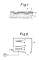
- Fig. l shows a longitudinal cross sectional view of an example of the optical recording media according to the present invention
- Fig. 2 shows an apparatus for producing the optical recording medium according to the present invention
- Fig. 3 shows a pattern of the temperature change to the transmission of the recording medium obtained in Example 4
- Fig. 4 shows the dependency of the C/N ratio of the recording medium obtained in Example ll on the recording laser power
- Fig. 5 shows the dependency of the C/N ratio of the recording medium obtained in Example l2 on the recording laser power.
- a plastic material such as acrylic resin, polycarbonate resin, etc., a metal such as aluminum, or glass as well as a material made by applying a thermosetting resin or photosetting resin on the above-mentioned substrate may be mentioned.
- the plastic substrate have a merit of being cheap in price, easy in processing and excellent in the optical properties.
- the recording medium according to the present invention a cheap plastic substrate is available since the birefringence change thereof is small, and is stabilized by annealing the recording medium of a high quality and a high cost-performance can be offered.
- a recording layer containing Te, Se and F is deposited onto the above-mentioned substrate by a reactive sputtering method.
- the recording layer containing Te, Se and F is deposited onto the substrate by providing a glow discharge in a vacuum chamber into which a gaseous mixture comprising argon gas and a selenium fluoride gas has been introduced while using an target material comprising Te or Te and Se, thereby providing the reactive sputtering.
- the thickness of the deposited recording layer made by sputtering is l50 to l000 ⁇ , preferably 200 to l000 ⁇ . In the case where the thickness thereof is less than l50 ⁇ , a satisfactory readout signal can not be obtained since a reflection from the recording layer is low, and in the case where the thickness thereof is more than l000 ⁇ , the recording sensitivity of the optical recording medium becomes poor.
- Te which is a component of the recording layer has been derived from the target material, and F which is also a component thereof has been derived from the fluoride gas, Se which is also a component thereof has been derived from the target material containing Te and Se or the selenium fluoride gas.
- the temperature of the substrate is necessary to maintain the temperature of the substrate at a temperature of an extent of from a room temperature to a sufficient lower temperature than the softening point of the substrate during deposition, for instance, at a temperature of an extent of from 40 to 50°C, in the case of using polycarbonate substrate.
- the above-mentioned temperature of the substrate is easily achieved even without cooling the substrate by a conventional magnetron-sputtering method.
- Te alone, an alloy comprising Te and Se, and an alloy comprising Te and Se as the main component and further containing Pb, Sb, Sn, In, Ge, etc. may be exemplified.
- pre-sputtering by an inert gas is generally carried out.
- the conditions of electric discharge at the time of carrying out the pre-sputtering and the time period thereof depend on the oxidized state of the surface of the target, it is necessary to carefully carrying out the pre-sputtering.
- the fluctuation of the sputtering rate owing to the oxidation of the surface of the target can be prevented, and as a result, there is an effect in preventing the fluctuation of the composition of the deposited films on the above-mentioned reactive sputtering.
- the alloy target containing Te and Se is easily prepared by an ordinary sintering method or melting method.
- the deposition of the recording layer of the optical recording medium is carried out by a conventional sputtering apparatus of radio frequency or direct current discharge while using the above-mentioned target.
- the effect of making the recording medium of Te contain Se is to prevent the degradation of the recording medium itself by oxidation.
- the content of Se in the target is preferably made to be from 5 to 30 atomic%.
- the surface tension of the recording medium at the time of melting thereof is reduced by containing of Se in the film materials, it is not favorable to make the target contain Se in an amount over 30 atomic% in the case of forming the pits by deforming the part locally irradiated by a laser beam while utilizing the surface tension of the film material.
- the amount of Se in the target is preferably made to be from l to 5 atomic%, and even by such a content of Se, there is an effect in preventing the oxidation of the surface of the target.
- the recording medium contain another element in addition to Te, Se and F
- a method of adding the objective element into target of Te alone or the alloy target containing Te and Se may be mentioned.
- Pb, Sb, Sn, In, Ge, etc. into the target containing Te and Se, if desired, the specific properties of the medium for recording can be controlled.
- Se2F2, SeF4 and SeF6 are mentioned as a selenium fluoride gas, SeF6 is generally used, and the ratio of the selenium fluoride gas in the gaseous mixture is selected in the range of from 0.l to 50% by volume.
- the amount of such a fourth component is preferably l to 20 atomic%.
- the oxidation resistance of the above-mentioned recording layer is poor and the stability thereof in the course of time becomes poor.
- the content of Se is more than 25 atomic%, the energy which is necessary for forming the holes parts is raised. Namely, the recording sensitivity becomes poor.
- the films do not take the non-crystalline structure, and in the case where the content of F is more than 40 atomic%, the substrate is apt to be damaged and moreover, the recording sensitivity becomes poor.
- the film according to the present invention takes an uniform non-crystalline structure.
- the reason why the deposited film according to the present invention takes a non-crystalline structure has not necessarily been clear, however, it is considered that since the molecules of the reactive gas according to the present invention contain fluorine atom(s), fluoride ions, fluorine radicals, and Se and Te fluorides are formed in the glow discharge plasma, these fluorides impinge onto the substrate together with the atoms of Te atom and Se atom, and at the same time, etching of the glowing surface of the films occur, resulting in the prevention of the growth of the large grain.
- the etching of the surface of the substrate slightly by the above-mentioned fluoride ions or fluorine radicals has also an effect of uniformalizing the adherence between the substrate and the deposited film.
- the deposited layer contains Se other than Te
- the oxidation-resistance which cannot be obtained by Te alone can be obtained and the reflectivity of the above-mentioned recording medium does not change at all even after beeing exposed to an accelerated test for 30 days at a temperature of 70°C and at a relative humidity of 85%.
- the micro-structure of the films is changed and as a result, it is able to increase the stability of the crystal, the recording sensitivity, the pit form, etc. in the course of time.
- the recording medium before annealing according to the present invention shows a uniform non-crystalline structure, and even after the annealing, it shows a stable polycrystalline structure of grain of less than l000 ⁇ in the diameter. Particularly, it is possible to make the grain size to not more than several hundred ⁇ , and the recording medium of the just-mentioned grain size does not cause any bad influence such as the occurrence of noise to the readout signal and the disorder of the shape of pits form at all.
- the non-crystalline structure mentioned in the present invention means the micro-structure showing the pattern of the usual X-ray diffraction method, in which pattern any clear crystal line peak cannot be obserbed, and further means the structure in which so-called micro-crystalline of the grain diameter of several tens ⁇ are present.
- the polycrystalline structure of the grain size of less than l000 ⁇ means all the micro-structures in which the largest grain size is less than l000 ⁇ , and therefore includes the non-crystalline structure, the microcrystalline structure, the polycrystalline structure and the hetero-structure as the mixture of the above-mentioned three structures. Such a structure can be confirmed accurately by observing the transmission image, the diffraction pattern or the lattice image of the deposited films with a transmission electron-microscopy.
- the annealing may be carried out in a vacuum, a dried air on a nitrogen atmosphere, however, in order to maintain the atmosphere in a uniform state, the dried air or a nitrogen atmosphere is preferable.
- the annealing is carried out in the atmosphere maintained at a temperature of higher than 60°C to less than l30°C, preferably 60°C to l00°C and more preferably 60°C to 90°C.
- the temperature of the annealing is sufficiently lower than the softening point of the plastic substrate, and for instance, a temperature of lower than 90°C is preferable in the case of annealing a substrate made of a polycarbonate resin.
- the annealing may be carried out in succession after finishing the sputtering at a higher temperature than that during deposition of the films, the treated substrate is usually taken out once from the sputtering vacuum system to be cooled to room temperature and then subjected to the annealing.
- the fluorine content in the deposited film decreases by the annealing, in order to obtain the above-mentioned stable and micro-structure after the annealing, since the fluorine atom effectively terminates dangling bond of Te, the fluorine content contained in the films is from 0.l to 30 atomic% after the annealing. It is preferable that the above-mentioned fluorine content is from l to 20 atomic%, and there is a tendency in which the grain diameter of the crystals is apt to be larger than l000 ⁇ after the annealing in the case where the fluorine content is below 0.l atomic%.
- the shapes of pits have serious irregularities and such a high content is not preferable. Still more, in the case where the fluorine content is more than 20 atomic%, there is a tendency of raising the crystallization temperature.
- the micro-structure in the above-mentioned recording layer is sufficiently stabilized by the annealing at a temperature of from not less than 60°C to less than l00°C, particularly at a temperature of not more than 90°C.
- the mixing ratio of the selenium fluoride gas and argon gas it is possible to control the amorphous-to-crystalline transition temperature of the recording medium according to the present invention within the above-mentioned range.
- the present invention it is possible to stabilize the birefringence value of the above-mentioned plastic substrate by carrying out the annealing.
- the noise due to the fluctuation of the readout signals derived from birefringence in a method of detecting the readout light through the substrate is reduced to the negligible extent.
- the recording layer has been diposited directly on the substrate as has been described above, it is also available to provide an underlayer between the substrate and the recording layer for the purposes of improving the recording sensitivity and the shape of pits, etc., and further, it is available to provide a protective layer on the above-mentioned recording medium for the protection of the recording medium. Particularly, it is effective to use an underlayer made of a fluorocarbon polymer.
- the underlayer of a fluorocarbon polymer various kind are considered corresponding to the performance required to the optical recording medium which is to be obtained.
- a dry-process in vacuum is favorable for producing the underlayer from the viewpoint of the uniformity of the layer, the decrease of pin-holes and the constitution of in-line process with the recording layer, and in the concrete, a plasma polymerized film of a fluorocarbon, a sputtered film of a polyfluorocarbon, a vacuum evaporated film of a polyfluorocarbon, etc. is exemplified.
- a fluorocarbon a perfluoroalkane such as CF4, C2F6, etc., a perfluoroalkene such as CF3CFCF2, perfluorohexane, perfluorobenzene, etc. may be exemplified.
- any fluorocarbon may be used even if it is a gas or a liquid at normal temperature, provided that the fluorocarbon has an adequately high vapour pressure, glow discharge can be sustained in a vacuum chamber after filling the chamber with the vapour of the fluorocarbon at a pressure of the order of higher than l0 ⁇ 3 Torr and the fluorocarbon has a high degree of substitution by fluorine.
- the plasma polymerized film of fluorocarbon can be formed by using the above-mentioned fluorocarbon as the monomer and using a capacitively coupled electric discharge or inductively coupled electric discharge.
- the films may be deposited by the sputtering of polytetrafluoroethylene, copolymer of tetrafluoroethylene and hexafluoropropylene, copolymer of tetrafluoroethylene and perfluoroalkoxyethylene, etc. in the gasous region such as argon gas, a gaseous mixture of the inert gas and the above-mentioned monomer, etc.
- gasous region such as argon gas, a gaseous mixture of the inert gas and the above-mentioned monomer, etc.
- the thickness of the underlayer of the fluorocarbon polymer is ordinally l00 to l000 ⁇ .
- the above-mentioned underlayer of the fluorocarbon polymer exerts an influence or the shape of pits, the presence or absence of remnants in the pits, the recording sensitivity of the recording medium, etc. according to the conditions of the interface between the above-mentioned underlayer and the recording layer. Accordingly, an exact evaluation concerning the composition and the structure of the underlayer surface of the fluorocarbon polymer, and a control thereof in the manufacturing step are important.
- the composition and the structure of the underlayer of fluorocarbon polymer was evaluated by the ESCA method.
- the kinds of the elements, their composition and the state of chemical bonding in the vicinity of the surface of the specimen can be analyzed from the energy spectrum of the photoelectron turned out of the atoms in the compound of the specimen by the irradiation of soft X-ray.
- the spectrum of the fluorine lS orbital(F lS ) and the spectrum of the carbon lS orbital(C lS ) on the surface of the thin film of fluorocarbon polymer before forming the recording layer thereon were determined while using the ESCA spectrometer of the type of "XSAM-800" made by SPECTROS Company.
- the spectrum F lS consists of a single peak having the center in the vicinity of 688 eV of binding energy
- the C lS spectrum consists of several peaks having the centers in the region of from 285 to 294 eV of binding energy.
- the peaks concerning the -CF3 group and the >CF2 groups can be discriminated particularly clearly from the other binding states.
- the peaks concerning the -CF3 group and the >CF2 groups may be identified by comparison with reference chemical shifts according to the method disclosed in literature (D.T. Clark and D. Shuttleworth, J. Poly. Sci., l8(80) page 27; K. Nakajima, A.T. Bell and M. Shen, J. Appl. Poly. Sci., 23(79) page 2627, etc.), the ratio of each integral peak area intensity to the whole integral intensity of C lS is calculated and the thus calculated ratios were made to be "-CF3/C" and ">CF2/C".
- -CF3/C is the ratio of carbon atoms forming the -CF3 groups to total carbon atoms
- >CF2/C is the ratio of carbon atoms forming the >CF2 groups to total carbon atoms.
- the ratio of the number of fluorine atoms to the number of carbon atoms can be calculated from the peak area ratio of C lS to F lS .
- compositions and the structure of the obtained underlayer of fluorocarbon polymer by the above-mentioned method and the specific properties of the optical recording medium, and furthermore the controlling method of the composition and the structure thereof are explained as follows. Then, it is easily to select the most suitable composition and structure of the underlayer of the fluorocarbon polymer along each kind of the recording layer containing Te, Se and F.
- the relationship between the composition of the underlayer of fluorocarbon polymer and the specific property as the optical recording medium are primarily due to the ratio (F/C) of the number of fluorine atoms to the number of carbon atoms in the surface of the underlayer which contacts to the recording layer.
- the F/C ratio is less than 0.9
- the effect of the improvement of the sensitivity is scarcely observed as compared to the case where the recording layer is deposited directly on the polycarbonate substrate.
- the power of the laser beam necessary for recording decreases monotonously, namely, the recording sensitivity is improved.
- the above-mentioned improvement of the recording sensitivity is saturated in the F/C ratio of not less than l.4.
- the F/C ratio is not less than l.4
- there are no remnants in the pits and the uniform pits having smooth and well-defined rim are formed without according to the difference of the process for producing the underlayer and of the detailed morphology of the underlayer surface, and a high C/N ratio (Carrier to Noise Ratio) can be attained. Accordingly, it is suitable for offering an optical recording medium particularly high in the sensitivity and the C/N ratio to make the F/C ratio not less than l.4.
- the F/C ratio is more than l.8 since the adhesion between the recording layer and the underlayer deteriorates, there is a tendency that the minimum size of the pits is apt to be enlarged in the case of forming the pits by the same laser power as compared to the case where the F/C ratio is not more than l.8. Namely, there is a limit of carrying out the recording of high density.
- the F/C ratio is not less than l.4, the adhesion is nearly constant and there is no effect of improving.
- the F/C ratio By making the F/C ratio to be less than l.4, the adhesion increase and it is possible to make the size of the pits small. Accordingly, by making the F/C ratio of not less than 0.9 to less than l.4, the recording of high density can be attained while improving the recording sensitivity.
- the F/C ratio is not less than 0.9 to less than l.4
- the remnants remain in the pits and the shapes of the rim reveal irregularities under conditions on preparing the layer of fluorocarbon polymer there are cases where a high C/N ratio can not be obtained in the case where the F/C ratio is not less than l.4 cannot be obtained
- the C/N ratio in case of the F/C ratio of not less than 0.9 to less than l.4 is superior to that in case of using no underlayer.
- the purpose is attained, in the C lS spectrum obtained by the ESCA method, by controlling the composition of the underlayer so that not less than l8 atomic% of the total carbon atoms construct the -CF3 groups and from not less than l8 to less than 40 atomic% of the total carbon atoms construct the >CF2 groups.
- the sensitivity is poor, and on the other hand, in the case where the amount thereof is too large, the size of the pits becomes too large. Namely, the above-mentioned these media are not suitable for the recording of high density.
- the amount of the -CF3 group is too small, remnants remain in the pits and the pit shape reveal irregularities. Since the irregularities are detected as the noise, the C/N ratio (Carrier to Noise Ratio) is low.
- the composition and structure of the underlayer comprising a thin layer of fluorocarbon polymer most suitable according to the above-mentioned results, it is necessary to take care of the combination of several recording layers and the combination with the driving system which effects the recording and readout.
- the thin layer of fluorocarbon polymer can be optimized flexibly by only changing the raw materials such as the gaseous monomer, the sputtering target etc. or by controlling the discharge conditions even in the case of using the same apparatus for fabricating the layer.
- the capacitively coupled plasma polymerization can be actualized by only exchanging the target of the sputtering apparatus taking the parallel electrode structure with the material which is not subjected to sputtering such as stainless steel, and in the same sputtering apparatus, the plasma polymerization of a monomeric fluorocarbon and the sputtering of polyfluorocarbon can be carried out.
- the above-mentioned method has a merit of having a large for selecting the process for production and the raw material. Furthermore, it is also easy to construct an in-line process including the process for preparing the recording layer by the reactive sputtering method.
- the sputtering of polyfluorocarbon (tetrafluoroethylene polymer, copolymer of tetrafluoroethylene and hexafluoropropylene, copolymer of tetrafluoroethylene and perfluoroalkoxyethylene, etc.) is carried out by introducing argon gas under a pressure of from 5 ⁇ l0 ⁇ 3 to l ⁇ l0 ⁇ 2 Torr between the parallel electrodes and applying an electric field of a radio frequency thereon.
- the plasma polymerization of a fluorocarbon is carried out by introducing a monomeric fluorocarbon under a pressure of from 5 ⁇ l0 ⁇ 3 to l ⁇ l0 ⁇ 2 Torr also between the parallel electrodes and applying an electric field of a radio frequency thereon.
- the vacuum evaporation may be carried out by an electric resistance heating method.
- the F/C ratio in the surface layer of fluorocarbon polymer obtained by using a capacitively coupled plasma polymerization apparatus depends on the monomeric gas, the form of the apparatus, the conditions of electric discharge and particularly, on the discharge power and the pressure of the gaseous monomer, and as the F/C ratio, those in the range of from 0.2 to l.5 are easily available. In the surface of fluorocarbon polymer layer obtained by sputtering, the F/C ratio is easily available in the range of from l.l to l.8.
- the radicals such as -CF3, >CF2, etc. are made to be generated in numbers as large as possible and made to impinge onto the glowing surface of the films. Or else, there is a method by which the growing surface of the thin layer of fluorocarbon polymer, which has once adhered to the substrate, is made not to be exposed to high energy particles (electrons and ions) in the plasma as far as possible.
- F/C ratio can be raised also by mixing a monomeric fluorocarbon such as CF4, C2F6, etc. with the inert gas such as argon gas, etc. which is used in the sputtering. Furthermore, F/C ratio can be raised by raising F/C ratio of the evaporated polyfluorocarbon in the vacuum evaporation method.
- a monomeric fluorocarbon such as CF4, C2F6, etc.
- the inert gas such as argon gas, etc. which is used in the sputtering.
- F/C ratio can be raised by raising F/C ratio of the evaporated polyfluorocarbon in the vacuum evaporation method.
- the substrate is established while avoiding the internal part of the coil, wherein the density of the plasma is high, and in the plasma polymerization method by the capacitively coupled electric discharge, the distance between the parallel electrodes is separated and the substrate is established on one of the electrodes, preferably on the electrode in the earth side.
- the rate of the >CF2 group and the -CF3 group can be relatively increased by using a lower electric power of discharge, a higher pressure of the gaseous substance and a higher flow rate of the gaseous substance.
- the ratio of the number of fluorine atoms to that of carbon atoms in the underlayer of fluorocarbon polymer, which contacts to the recording layer, is 0.9 to l.8, and further not less than l8 atomic% of the total carbon atoms are preferably made to constitute the -CF3 group and further, from not less than l8 atomic% to less than 40 atomic% of the total carbon atoms are preferably made to constitute the >CF2 group. Namely, it is necessary to control the fine structure thereof shown by ESCA spectrum.
- the structures of the plasma polymerized layer of fluorocarbon and the sputtered layer of fluorocarbon polymer reflect those of the gaseous monomer and the target material to a certain extent.
- the -CF3 groups are contained in a large amount in the gaseous monomer or in the case where the -CF3 groups are rich in the radicals and the ions generated in the plasma, the -CF3 groups are apt to be taken into the polymerized layer.
- the layer deposited by sputtering of polytetrafluoroethylene also reflects the structure of the target and contains the >CF2 group in a large amount, however, the ratio of the -CF3 group can be raised also by carrying out the reactive sputtering with a gaseous mixture obtained by mixing hexafluoropropylene or carbon tetrafluoride with argon gas.
- a structure which fulfills the requisites of the present invention has been obtained in the conditions of the pressure of 5 ⁇ l0 ⁇ 3 to l ⁇ l0 ⁇ 2 Torr, the flow rate of the gas of 300 to 500 cc/min (determined by capillary-type flow meter set up for argon gas) and the electric power of discharge in the range of from l00 to 200 W.
- the electric discharge conditions depend on the shape and performances of the using apparatus (size and shape of the vacuum chamber, vent property, introducing method of the reactive gas, and shape, size and structure of the electrodes). Accordingly, in the above-mentioned description and Examples, concrete values of a gas pressure at the electric discharge, flow rate, electric discharge power, etc. are to be optimalized according to individual apparatus, and the present invention is not limited by the above-mentioned concrete values. Further, in the case of using the apparatus having the same shape, size, structure and performances, it is easily to have reproducibility.
- a layer of chlorofluorocarbon polymer may be used as the underlayer.
- the thin layer of chlorofluorocarbon is available by the sputtering of polychlorotrifluoroethylene, the reactive sputtering of polytetrafluoroethylene in a gaseous mixture of argon gas and a chlorofluorocarbon gas such as FRON ll3 (CCl2F - CClF2) or the plasma treatment by chlorofluorocarbon of the surface of the deposited layer by sputtering of polytetrafluoroethylene. Furthermore, the thin layer of chlorofluorocarbon is available by carrying out plasma polymerization while using the chlorofluorocarbon gas as the monomer.
- the thickness of the above-mentioned layer is generally from 20 to l000 ⁇ .
- the composition of the surface of the underlayer, which contacts to the recording layer is made to be the above-mentioned composition and it is not necessary to make the composition of the whole underlayer to be the above-mentioned composition.
- the adhesion can be improved, the shortest pit length is shortened and on the other hand, the high sensitivity and the improvement of the shape of pit can be achieved.
- the plasma treatment is utilized and the recording layer is an alloy containing Te and Se
- the surface tension of the surface of the layer of fluorocarbon polymer becomes larger, and moreover, due to the crosslinking of carbon atoms, the density and the molecular weight of the crosslinked layer in the surface of the layer of fluorocarbon polymer are raised.
- Every one of the above-mentioned changes of the surface layer has an effect of raising the adhesion between the recording layer and the underlayer.
- the thickness and the degree of crosslinking of the above-mentioned surface layer can be controlled by the condition of plasma discharge, particularly by the power of discharge and the time period of exposure to the plasma and the distance between the substrate and the electrode, and as a result, it is possible to control and adhesion of the recording layer to the underlayer broadly and to set each kind of the recording layer in the optimum state.
- a sputtered layer of polytetrafluoroethylene (PTFE) was prepared, and the layer was subjected to the plasma treatment by argon plasma under a pressure of 5 ⁇ l0 ⁇ 3 Torr at a discharge power of l00 W, and thereafter the contact angle of the layer and the atomic ratio (F/C) of fluorine atom to carbon atom within l0 nm from the surface of the layer were measured according to the ESCA method.
- the determination of the atomic ratio (F/C) by the ESCA method was carried out as that described before.
- Fig. 2 shows one example of the apparata for producing the medium for optical recording medium according to the present invention by the reactive sputtering method.
- (5) is a vacuum chamber
- (6) are cathode and anode electrodes
- (7) is a target of an alloy containing Te and Se
- (8) is a substrate
- (9) is a gas inlet
- (l0) is a shutter
- (ll) is an exhaust gas outlet.
- the vacuum chamber (5) was evacuated to the back pressure of the order of l0 ⁇ 6 Torr and then, argon gas was introduced into the chamber (5) from the gas inlet (9) to raise the inner pressure of the chamber (5) to 5 ⁇ l0 ⁇ 3 Torr.
- a radio frequency voltage at l3.56 MHz was continuously applied between the electrodes (6) to cause glow discharge, and the above-mentioned state was kept for about l0 min to clean the surface of the target (7).
- the inner space of the chamber (5) was evacuated again to the extent of l0 ⁇ 6 Torr, and a gaseous mixture of 90% by volume of argon and l0% by volume of gaseous SeF6 was introduced into the chamber (5) from the gas inlet (9) to make the total pressure to 5 ⁇ l0 ⁇ 3 Torr. Thereafter, by applying a radio frequency voltage of 50 W at l3.56 MHz between the anodic electrode (6) on the side of the substrate and the cathodic electrode (6) on the side of the target (7), thereby a glow discharge was caused for carrying out the sputtering.
- an alloy of 88 atomic % of Te and l2 atomic % of Se was used, and a sputtered layer of 40 nm in thickness was deposited on the substrate.
- the content of Se in the thus deposited layer was l5 atomic %, and the content of fluorine atom therein was 20 atomic %.
- the recording and reading-out were carried out on the thus produced optical recording medium by a semiconductor laser diode of wave length of 830 nm (pulse width of 500 n sec). A sensitivity of 4mW and a C/N ratio (Carrier to noise ratio) of 52 dB were obtained.
- argon gas was introduced to a pressure of l ⁇ l0 ⁇ 2 Torr, and by causing a glow discharge at l00 W of a high frequency electric power of l3.56 MHz, a sputtered layer (F/C ratio of l.6) of about l50 ⁇ was made to deposite on a substrate of polycarbonate resin.
- the electrode of the side of the substrate was moved to right over the alloy target made of 88% of Te and l2% of Se, and after carrying out pre-sputtering, SeF6 gas was introduced into the chamber in a volume ratio of l0% to make the total pressure in the chamber to 5 ⁇ l0 ⁇ 3 Torr. Thereafter, by applying a radio frequency voltage of 50 W at l3.56 MHz between the electrode on the side of the substrate and the electrode on the side of the target, thereby a glow discharge was caused for carrying out the sputtering. A sputtering layer of 40 nm in thickness was deposited on the substrate. The content of Se in the thus deposited layer was l5 atomic %, and the content of fluorine atom therein was 20 atomic %.
- Fig. l shows a longitudinal cross sectional view of the thus obtained optical recording medium.
- (l) is a substrate
- (2) is an underlayer
- (3) is a recording layer
- (4) is a channel for track-servo.
- argon gas was introduced into the vacuum chamber and a glow discharge was caused between the substrate and the target by a radio frequency voltage of 50 W at l3.56 MHz.
- the target an alloy of 85 atomic % of Te and l5 atomic % of Se was used, and a Te-Se deposite layer of 400 ⁇ in thickness was formed on the substrate.
- the C/N ratio was 45 dB.
- the recording sensitivity was 4.5 mW. There were local irregularity of recording sensitivity.
- the C/N ratio was only 45 dB.
- the recording sensitivity was 4 mW.
- the vacuum chamber was evacuated to the extent of l0 ⁇ 6 Torr, and then SeF6 gas to argon gas was introduced thereinto at a flow ratio shown in Table l, and by applying a high frequency voltage between the electrodes in the same manner as in Example l, an electric discharge was caused.
- the discharge power and the pressure within the vacuum chamber were the same as shown in Table l. Further, glass substrates of a thickness of l2 mm were used. The thickness of each of the deposited layer by sputtering was from 300 to 400 ⁇ . The fluorine content (shown by atomic %) of the layer after annealing was the same as that shown in Table l. In order to evaluate the annealing temperature necessary for stabilizing the crystal structure of the deposited layer by sputtering, the dependencies of the transmission of recording layer on temperature were measured. As an example of the pattern of the temperature change of the transmission, the pattern of a specimen of Example 4 in Table l in the case of raising a temperature at l3°C/min is shown in Fig. 3.
- the medium for recording of Examples 4 and 5 and Comparative Example 2 and 3 was formed on the disk-shaped substrate of polycarbonate resin, wherein a hexafluoropropylene polymer as an underlayer was formed on the disk-shaped substrate of polycarbonate resin, and the change of the specific properties of the disk was examined before and after annealing, which was carried out in the air at 80°C for one hour.
- Example 4 a stabilized and uniform micro-structure was formed by annealing, and it does not give any unfavorable effects such as noises in the readout signal. Further, there was no local irregularity of the sensitivity and the uniform pits were formed. As a result, an improvement of from 2 to 3 dB of C/N ratio (carrier to noise ratio) was effected.
- the grain size of the polycrystalline of the recording medium according to the present invention was externally small, and it was possible to control the crystallization temperature, particularly to not less than 90°C.
- the optical specific properties were quite stable in the accelerated test at 65°C and 80% RH. Also, on examining the change in quality of the recording medium due to the repeated irradiation on the same track by the readout light, the degradation in quality of the medium before annealing began by the power of readout laser beam of l.3 mW and the accurate readout was impossible, however, on the other hand, the quality of the medium was quite stable after the annealing.
- Example 6 the annealing at a temperature of not less than 90°C was necessary in order to obtain the same effect as above, and such medium was not suitable for use of the substrate of polycarbonate resin, wherein a hexafluoropropylene polymer as an underlayer was formed on the disk-shaped substrate of polycarbonate resin.
- Each of several underlayers of fluorocarbon polymer shown in Table 2 was provided on a substrate (l30 mm in diameter and l.2 mm in thickness) of polycarbonate resin by the sputtering method or the plasma polymerization method.
- the sputtering by the fluorocarbon polymer (tetrafluoroethylene resin, copolymer of tetrafluoroethylene and hexafluoropropylene or copolymer of tetrafluoroethylene and perfluoroalkoxyethylene) was carried out by introducing argon gas under a pressure range of from 5 ⁇ l0 ⁇ 3 to l ⁇ l0 ⁇ 2 Torr between the parallel electrodes and applying a radio frequency voltage of from 50 to 200 W at l3.56 MHz.
- the plasma polymerization of the fluorocarbon (tetrafluoroethylene or hexafluoropropylene) was carried out by also introducing the gaseous monomer under a pressure range of from 5 ⁇ l0 ⁇ 3 to l ⁇ l0 ⁇ 2 Torr between the parallel electrodes and applying a radio frequency voltage of from l00 to 600 W at l3.56 MHz.
- the reactive sputtering was carried out on the underlayer while using an alloy target consisting of 88% of Te and l2% of Se and introducing SeF6 gas and argon gas in the same manner as in Example l, thereby a recording layer of a thickness of about 400 ⁇ was formed.
- the composition of the thus obtained layers is the same as that of Example l
- F/C, CF3/C, CF2/C, the presence or absence of the remnants in the pits and the recording sensitivity of the thus obtained recording media were measured, the results being shown in Table 2.
- the recording and reading-out was carried out by a semiconductor laser beam while using the above-mentioned optical recording medium prepared on a disk-shaped substrate of polycarbonate resin of l30 mm in diameter.
- the power of the laser beam necessary for writing was taken as the recording sensitivity.
- the shapes of the thus formed pits were observed by a scanning electron microscopy (SEM) and the presence or absence of the remnants in the pit.
- the rim of the pit was well-defined without any irregularity and the C/N ratio of the optical recording medium was improved by a few dB as compared to the case where the remnants were present.
- Te88Se12 As the recording layer on the thus formed underlayer in a gaseous mixture of argon and SeF6, a medium of TeSe-SeF6 series (consisting of l5 atomic% of Se, 20 atomic % of F and the balance of Te and having a thickness of 400 ⁇ ) was prepared. On the thus prepared optical recording medium, the evaluation of the writing and reading-out properties was carried out under the following conditions.
- the disk-shaped substrate was rotated at l800 rpm, and the recording and reading-out were carried out on the tracks of the radius of about 30 mm from the rotating axis by a semiconductor laser diode of a wave length of 830 nm.
- the recording was carried out by a pulse light of l.0 MHz and duty of 50 %.
- Fig. 4 (a) The dependency of C/N ratio (carrier to noise ratio) on the recording power is shown in Fig. 4 (a).
- the C/N ratio was larger than 55 dB and showed a stable specific property within a broad range of the recording power. On carrying out the SEM observation, any remnant could scarcely be found in the pits.
- FIG. 4 (b) and (c) respectively show the dependency of C/N ratio on the recording power in the cases of forming the same recording layer as in Example 2 on the underlayer of polytetrafluororethylene by sputtering wherein the ratio of the number of fluorine atoms to the number of carbon atoms was l.5 [in the case of (b)] and l.25 [in the case of (c)]. Also in Fig. 4, (d) shows the case where the recording layer was directly formed on the substrate of polycarbonate without using an underlayer.
- FIG. 4 shows the case wherein a reactive sputtering of polychlorotrifluoroethylene was carried out in a gaseous mixture of argon gas and CCl2F-CClF2 to form a layer in which the ratio of the number of fluorine atoms to the number of carbon atoms was 0.85 and which contains l9 atomic % of chlorine, as the underlayer.
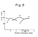
- a sputtering of polytetrafluoroethylene (PTFE) was carried out under a pressure of argon gas of l ⁇ l0 ⁇ 2 Torr and at a discharge power of 200 W to form a thin layer of a thickness of about 200 ⁇ on a disk-shaped substrate of polycarbonate resin. Thereafter, the thus prepared material was subjected to plasma treatment under a pressure of argon gas of 5 ⁇ l0 ⁇ 3 Torr at a discharge power of 50W for 30 sec.
- PTFE polytetrafluoroethylene
- Fig. 5 shows the dependency of C/N ratio on the recording power.
- a1 shows the case of the underlayer which has not been treated in the plasma
- b1 shows the case of the plasma treated underlayer
- c1 shows the case of without having the underlayer.
- the sensitivity of the medium b1 was more improved than the sensitivity of the medium c1
- C/N ratio of the medium of b1 was larger than C/N ratio of the medium of a1 by from 2 to 3 dB
- the dependency of C/N ratio of the medium of b1 on the recording power is smaller than that of the medium of a1. It was found as the result of observation of SEM that the above-mentioned facts were due to the relatively slight increase of the pit size in the medium of b1 in contrast to the rapid increase of the pit size in the medium of a1 with the increase of the recording power.
- the amount of the remnants in the pits was smaller in b1 than in c1, and a uniform rim was formed in b1.
- the plasma treating conditions for obtaining the optimized property as b1 can be decided by the ESCA method.
- the treating conditions and the treating time period so that the ratio of the number of fluorine atoms to the number of carbon atoms in the layer within l0 nm from the treated surface is from l.0 to l.2.
- a substrate of polymethyl methacrylate resin (PMMA) or polycarbonate resin (PC) which had been preliminarily washed was set in a vacuum room, and after evacuating to about l ⁇ l0 ⁇ 6 Torr, 20 cc/min of argon (determined by capillary-type flow meter) and 5 cc/min of SeF6 (determined by capillary-type flow meter set up for argon) were introduced into the room to raise the inner pressure thereof to about 5 ⁇ l0 ⁇ 3 Torr.
- Te was used as a target material.
- a deposited layer of about 250 ⁇ in thickness was obtained.
- the pits were formed by the pulse width of 200 nsec, and on the layer deposited on the PC substrate, the pits were formed by the pulse width of 250 nsec.
- the light reflectivity (in the extent of 30%) at 830 nm did not show any change before and after the acceleration.
Landscapes
- Chemical & Material Sciences (AREA)
- Inorganic Chemistry (AREA)
- Engineering & Computer Science (AREA)
- Manufacturing & Machinery (AREA)
- Thermal Transfer Or Thermal Recording In General (AREA)
- Manufacturing Optical Record Carriers (AREA)
Applications Claiming Priority (16)
| Application Number | Priority Date | Filing Date | Title |
|---|---|---|---|
| JP61095264A JPS62252543A (ja) | 1986-04-24 | 1986-04-24 | 光学的記録用媒体 |
| JP95264/86 | 1986-04-24 | ||
| JP142167/86 | 1986-06-18 | ||
| JP61142167A JPS62298944A (ja) | 1986-06-18 | 1986-06-18 | 光学的記録用媒体 |
| JP61220833A JPS6374139A (ja) | 1986-09-18 | 1986-09-18 | 光学的記録用媒体 |
| JP220833/86 | 1986-09-18 | ||
| JP302607/86 | 1986-12-18 | ||
| JP61302607A JPS63155443A (ja) | 1986-12-18 | 1986-12-18 | 光学的記録用媒体 |
| JP306073/86 | 1986-12-22 | ||
| JP61306073A JPS63160027A (ja) | 1986-12-22 | 1986-12-22 | 光学的記録用媒体 |
| JP307120/86 | 1986-12-23 | ||
| JP61307120A JPS63160031A (ja) | 1986-12-23 | 1986-12-23 | 光学的記録用媒体 |
| JP2966/87 | 1987-01-09 | ||
| JP62002966A JPS63171446A (ja) | 1987-01-09 | 1987-01-09 | 光学的記録用媒体の製造方法 |
| JP62013650A JPS63182188A (ja) | 1987-01-23 | 1987-01-23 | 光学的記録用媒体 |
| JP13650/87 | 1987-01-23 |
Publications (3)
| Publication Number | Publication Date |
|---|---|
| EP0242942A2 true EP0242942A2 (de) | 1987-10-28 |
| EP0242942A3 EP0242942A3 (en) | 1988-11-09 |
| EP0242942B1 EP0242942B1 (de) | 1992-01-29 |
Family
ID=27571484
Family Applications (1)
| Application Number | Title | Priority Date | Filing Date |
|---|---|---|---|
| EP87301046A Expired - Lifetime EP0242942B1 (de) | 1986-04-24 | 1987-02-05 | Optisches Aufzeichnungsmedium und Verfahren zu dessen Herstellung |
Country Status (3)
| Country | Link |
|---|---|
| EP (1) | EP0242942B1 (de) |
| KR (1) | KR910009072B1 (de) |
| DE (1) | DE3776386D1 (de) |
Cited By (1)
| Publication number | Priority date | Publication date | Assignee | Title |
|---|---|---|---|---|
| EP0405450A3 (en) * | 1989-06-30 | 1991-08-21 | Kabushiki Kaisha Toshiba | Data recording medium and method of manufacturing the same |
Families Citing this family (1)
| Publication number | Priority date | Publication date | Assignee | Title |
|---|---|---|---|---|
| DE60309232T2 (de) | 2002-03-05 | 2007-09-06 | Mitsubishi Kagaku Media Co. Ltd. | Phasenwechselaufzeichnungsmaterial für ein Informationsaufzeichnungsmedium und ein Informationsaufzeichnungsmedium dieses verwendend |
Family Cites Families (1)
| Publication number | Priority date | Publication date | Assignee | Title |
|---|---|---|---|---|
| DE2718157A1 (de) * | 1977-04-23 | 1978-11-02 | Licentia Gmbh | Verfahren zum herstellen eines elektrophotographischen aufzeichnungsmaterials |
-
1987
- 1987-02-05 KR KR1019870000966A patent/KR910009072B1/ko not_active Expired
- 1987-02-05 DE DE8787301046T patent/DE3776386D1/de not_active Expired - Lifetime
- 1987-02-05 EP EP87301046A patent/EP0242942B1/de not_active Expired - Lifetime
Cited By (1)
| Publication number | Priority date | Publication date | Assignee | Title |
|---|---|---|---|---|
| EP0405450A3 (en) * | 1989-06-30 | 1991-08-21 | Kabushiki Kaisha Toshiba | Data recording medium and method of manufacturing the same |
Also Published As
| Publication number | Publication date |
|---|---|
| EP0242942A3 (en) | 1988-11-09 |
| KR910009072B1 (ko) | 1991-10-28 |
| EP0242942B1 (de) | 1992-01-29 |
| KR870010504A (ko) | 1987-11-30 |
| DE3776386D1 (de) | 1992-03-12 |
Similar Documents
| Publication | Publication Date | Title |
|---|---|---|
| US4839207A (en) | Optical recording medium and process for producing the same | |
| EP0059096B1 (de) | Informations-Aufzeichnungsmaterial | |
| US5102708A (en) | Data recording medium and method of manufacturing the same | |
| US4786538A (en) | Optical recording medium formed of chalcogenide oxide and method for producing the same | |
| EP0242942A2 (de) | Optisches Aufzeichnungsmedium und Verfahren zu dessen Herstellung | |
| US4973520A (en) | Optical recording medium | |
| EP0371428A2 (de) | Medium für Informationsspeicherung | |
| JPH01196743A (ja) | 情報記録媒体 | |
| CA1258974A (en) | Optical recording medium and process for producing the same | |
| JPH0379772B2 (de) | ||
| JPH0462556B2 (de) | ||
| EP0339889A2 (de) | Medium für optische Aufzeichnung und Verfahren zu dessen Herstellung | |
| JPH0511559B2 (de) | ||
| JPH0444811B2 (de) | ||
| JPS59198543A (ja) | 光記録用媒体とその作製方法 | |
| JP2673281B2 (ja) | 光記録媒体の製造方法 | |
| JP2825059B2 (ja) | 光ディスク及びその製造方法 | |
| JP2731202B2 (ja) | 情報記録媒体 | |
| JPS6374139A (ja) | 光学的記録用媒体 | |
| US5061597A (en) | Optical recording media and process for preparing same | |
| JPH0248990A (ja) | 光記録媒体およびその製造方法 | |
| EP0338862A2 (de) | Medium für optische Aufzeichnung und Verfahren zu dessen Herstellung | |
| JPS60147392A (ja) | 光情報記録媒体 | |
| JPH087879B2 (ja) | 光学的記録用媒体 | |
| JPH06223408A (ja) | 光学的情報記録用媒体 |
Legal Events
| Date | Code | Title | Description |
|---|---|---|---|
| PUAI | Public reference made under article 153(3) epc to a published international application that has entered the european phase |
Free format text: ORIGINAL CODE: 0009012 |
|
| AK | Designated contracting states |
Kind code of ref document: A2 Designated state(s): DE FR GB IT NL |
|
| PUAL | Search report despatched |
Free format text: ORIGINAL CODE: 0009013 |
|
| AK | Designated contracting states |
Kind code of ref document: A3 Designated state(s): DE FR GB IT NL |
|
| RAP1 | Party data changed (applicant data changed or rights of an application transferred) |
Owner name: MITSUBISHI KASEI CORPORATION |
|
| 17P | Request for examination filed |
Effective date: 19890308 |
|
| 17Q | First examination report despatched |
Effective date: 19901018 |
|
| GRAA | (expected) grant |
Free format text: ORIGINAL CODE: 0009210 |
|
| AK | Designated contracting states |
Kind code of ref document: B1 Designated state(s): DE FR GB IT NL |
|
| ITF | It: translation for a ep patent filed | ||
| REF | Corresponds to: |
Ref document number: 3776386 Country of ref document: DE Date of ref document: 19920312 |
|
| ET | Fr: translation filed | ||
| PLBE | No opposition filed within time limit |
Free format text: ORIGINAL CODE: 0009261 |
|
| STAA | Information on the status of an ep patent application or granted ep patent |
Free format text: STATUS: NO OPPOSITION FILED WITHIN TIME LIMIT |
|
| 26N | No opposition filed | ||
| PGFP | Annual fee paid to national office [announced via postgrant information from national office to epo] |
Ref country code: FR Payment date: 19971217 Year of fee payment: 12 |
|
| PGFP | Annual fee paid to national office [announced via postgrant information from national office to epo] |
Ref country code: GB Payment date: 19971222 Year of fee payment: 12 |
|
| PGFP | Annual fee paid to national office [announced via postgrant information from national office to epo] |
Ref country code: NL Payment date: 19971231 Year of fee payment: 12 |
|
| PGFP | Annual fee paid to national office [announced via postgrant information from national office to epo] |
Ref country code: DE Payment date: 19980331 Year of fee payment: 12 |
|
| PG25 | Lapsed in a contracting state [announced via postgrant information from national office to epo] |
Ref country code: GB Free format text: LAPSE BECAUSE OF NON-PAYMENT OF DUE FEES Effective date: 19990205 |
|
| PG25 | Lapsed in a contracting state [announced via postgrant information from national office to epo] |
Ref country code: NL Free format text: LAPSE BECAUSE OF NON-PAYMENT OF DUE FEES Effective date: 19990901 |
|
| GBPC | Gb: european patent ceased through non-payment of renewal fee |
Effective date: 19990205 |
|
| PG25 | Lapsed in a contracting state [announced via postgrant information from national office to epo] |
Ref country code: FR Free format text: LAPSE BECAUSE OF NON-PAYMENT OF DUE FEES Effective date: 19991029 |
|
| PG25 | Lapsed in a contracting state [announced via postgrant information from national office to epo] |
Ref country code: DE Free format text: LAPSE BECAUSE OF NON-PAYMENT OF DUE FEES Effective date: 19991201 |
|
| REG | Reference to a national code |
Ref country code: FR Ref legal event code: ST |
|
| PG25 | Lapsed in a contracting state [announced via postgrant information from national office to epo] |
Ref country code: IT Free format text: LAPSE BECAUSE OF NON-PAYMENT OF DUE FEES Effective date: 20050205 |