EP0241317A2 - Herstellungsverfahren einer niedergeschlagenen Schicht - Google Patents
Herstellungsverfahren einer niedergeschlagenen Schicht Download PDFInfo
- Publication number
- EP0241317A2 EP0241317A2 EP87303225A EP87303225A EP0241317A2 EP 0241317 A2 EP0241317 A2 EP 0241317A2 EP 87303225 A EP87303225 A EP 87303225A EP 87303225 A EP87303225 A EP 87303225A EP 0241317 A2 EP0241317 A2 EP 0241317A2
- Authority
- EP
- European Patent Office
- Prior art keywords
- film
- deposited film
- process according
- substrate
- formation
- Prior art date
- Legal status (The legal status is an assumption and is not a legal conclusion. Google has not performed a legal analysis and makes no representation as to the accuracy of the status listed.)
- Granted
Links
Images


Classifications
-
- C—CHEMISTRY; METALLURGY
- C23—COATING METALLIC MATERIAL; COATING MATERIAL WITH METALLIC MATERIAL; CHEMICAL SURFACE TREATMENT; DIFFUSION TREATMENT OF METALLIC MATERIAL; COATING BY VACUUM EVAPORATION, BY SPUTTERING, BY ION IMPLANTATION OR BY CHEMICAL VAPOUR DEPOSITION, IN GENERAL; INHIBITING CORROSION OF METALLIC MATERIAL OR INCRUSTATION IN GENERAL
- C23C—COATING METALLIC MATERIAL; COATING MATERIAL WITH METALLIC MATERIAL; SURFACE TREATMENT OF METALLIC MATERIAL BY DIFFUSION INTO THE SURFACE, BY CHEMICAL CONVERSION OR SUBSTITUTION; COATING BY VACUUM EVAPORATION, BY SPUTTERING, BY ION IMPLANTATION OR BY CHEMICAL VAPOUR DEPOSITION, IN GENERAL
- C23C16/00—Chemical coating by decomposition of gaseous compounds, without leaving reaction products of surface material in the coating, i.e. chemical vapour deposition [CVD] processes
- C23C16/22—Chemical coating by decomposition of gaseous compounds, without leaving reaction products of surface material in the coating, i.e. chemical vapour deposition [CVD] processes characterised by the deposition of inorganic material, other than metallic material
- C23C16/24—Deposition of silicon only
-
- C—CHEMISTRY; METALLURGY
- C23—COATING METALLIC MATERIAL; COATING MATERIAL WITH METALLIC MATERIAL; CHEMICAL SURFACE TREATMENT; DIFFUSION TREATMENT OF METALLIC MATERIAL; COATING BY VACUUM EVAPORATION, BY SPUTTERING, BY ION IMPLANTATION OR BY CHEMICAL VAPOUR DEPOSITION, IN GENERAL; INHIBITING CORROSION OF METALLIC MATERIAL OR INCRUSTATION IN GENERAL
- C23C—COATING METALLIC MATERIAL; COATING MATERIAL WITH METALLIC MATERIAL; SURFACE TREATMENT OF METALLIC MATERIAL BY DIFFUSION INTO THE SURFACE, BY CHEMICAL CONVERSION OR SUBSTITUTION; COATING BY VACUUM EVAPORATION, BY SPUTTERING, BY ION IMPLANTATION OR BY CHEMICAL VAPOUR DEPOSITION, IN GENERAL
- C23C16/00—Chemical coating by decomposition of gaseous compounds, without leaving reaction products of surface material in the coating, i.e. chemical vapour deposition [CVD] processes
- C23C16/44—Chemical coating by decomposition of gaseous compounds, without leaving reaction products of surface material in the coating, i.e. chemical vapour deposition [CVD] processes characterised by the method of coating
- C23C16/448—Chemical coating by decomposition of gaseous compounds, without leaving reaction products of surface material in the coating, i.e. chemical vapour deposition [CVD] processes characterised by the method of coating characterised by the method used for generating reactive gas streams, e.g. by evaporation or sublimation of precursor materials
- C23C16/452—Chemical coating by decomposition of gaseous compounds, without leaving reaction products of surface material in the coating, i.e. chemical vapour deposition [CVD] processes characterised by the method of coating characterised by the method used for generating reactive gas streams, e.g. by evaporation or sublimation of precursor materials by activating reactive gas streams before their introduction into the reaction chamber, e.g. by ionisation or addition of reactive species
-
- H—ELECTRICITY
- H10—SEMICONDUCTOR DEVICES; ELECTRIC SOLID-STATE DEVICES NOT OTHERWISE PROVIDED FOR
- H10P—GENERIC PROCESSES OR APPARATUS FOR THE MANUFACTURE OR TREATMENT OF DEVICES COVERED BY CLASS H10
- H10P14/00—Formation of materials, e.g. in the shape of layers or pillars
- H10P14/20—Formation of materials, e.g. in the shape of layers or pillars of semiconductor materials
- H10P14/24—Formation of materials, e.g. in the shape of layers or pillars of semiconductor materials using chemical vapour deposition [CVD]
-
- H—ELECTRICITY
- H10—SEMICONDUCTOR DEVICES; ELECTRIC SOLID-STATE DEVICES NOT OTHERWISE PROVIDED FOR
- H10P—GENERIC PROCESSES OR APPARATUS FOR THE MANUFACTURE OR TREATMENT OF DEVICES COVERED BY CLASS H10
- H10P14/00—Formation of materials, e.g. in the shape of layers or pillars
- H10P14/20—Formation of materials, e.g. in the shape of layers or pillars of semiconductor materials
- H10P14/29—Formation of materials, e.g. in the shape of layers or pillars of semiconductor materials characterised by the substrates
- H10P14/2901—Materials
- H10P14/2922—Materials being non-crystalline insulating materials, e.g. glass or polymers
-
- H—ELECTRICITY
- H10—SEMICONDUCTOR DEVICES; ELECTRIC SOLID-STATE DEVICES NOT OTHERWISE PROVIDED FOR
- H10P—GENERIC PROCESSES OR APPARATUS FOR THE MANUFACTURE OR TREATMENT OF DEVICES COVERED BY CLASS H10
- H10P14/00—Formation of materials, e.g. in the shape of layers or pillars
- H10P14/20—Formation of materials, e.g. in the shape of layers or pillars of semiconductor materials
- H10P14/32—Formation of materials, e.g. in the shape of layers or pillars of semiconductor materials characterised by intermediate layers between substrates and deposited layers
- H10P14/3202—Materials thereof
- H10P14/3204—Materials thereof being Group IVA semiconducting materials
- H10P14/3211—Silicon, silicon germanium or germanium
-
- H—ELECTRICITY
- H10—SEMICONDUCTOR DEVICES; ELECTRIC SOLID-STATE DEVICES NOT OTHERWISE PROVIDED FOR
- H10P—GENERIC PROCESSES OR APPARATUS FOR THE MANUFACTURE OR TREATMENT OF DEVICES COVERED BY CLASS H10
- H10P14/00—Formation of materials, e.g. in the shape of layers or pillars
- H10P14/20—Formation of materials, e.g. in the shape of layers or pillars of semiconductor materials
- H10P14/34—Deposited materials, e.g. layers
- H10P14/3402—Deposited materials, e.g. layers characterised by the chemical composition
- H10P14/3404—Deposited materials, e.g. layers characterised by the chemical composition being Group IVA materials
- H10P14/3411—Silicon, silicon germanium or germanium
-
- H—ELECTRICITY
- H10—SEMICONDUCTOR DEVICES; ELECTRIC SOLID-STATE DEVICES NOT OTHERWISE PROVIDED FOR
- H10P—GENERIC PROCESSES OR APPARATUS FOR THE MANUFACTURE OR TREATMENT OF DEVICES COVERED BY CLASS H10
- H10P14/00—Formation of materials, e.g. in the shape of layers or pillars
- H10P14/20—Formation of materials, e.g. in the shape of layers or pillars of semiconductor materials
- H10P14/34—Deposited materials, e.g. layers
- H10P14/3438—Doping during depositing
- H10P14/3441—Conductivity type
- H10P14/3442—N-type
-
- H—ELECTRICITY
- H10—SEMICONDUCTOR DEVICES; ELECTRIC SOLID-STATE DEVICES NOT OTHERWISE PROVIDED FOR
- H10P—GENERIC PROCESSES OR APPARATUS FOR THE MANUFACTURE OR TREATMENT OF DEVICES COVERED BY CLASS H10
- H10P14/00—Formation of materials, e.g. in the shape of layers or pillars
- H10P14/20—Formation of materials, e.g. in the shape of layers or pillars of semiconductor materials
- H10P14/34—Deposited materials, e.g. layers
- H10P14/3438—Doping during depositing
- H10P14/3441—Conductivity type
- H10P14/3444—P-type
Definitions
- This invention relates to a process for forming a functional deposited film containing silicon, particularly a deposited film of polycrystalline silicon to be used for semiconductor devices, photosensitive devices for electrophotography, line sensors for image input, image pickup devices, etc.
- the normal pressure CVD method, the LPCVD method, the plasma CVD method, etc. have been primarily used, and, in general, the LPCVD method has been widely been used and industrialized.
- the substrate temperature is high and glass substrated, etc., which are cheap cannot be used, and deposited film having practically useful characteristics cannot be obtained at low temperature.
- the present invention provides a novel process for formation of a polycrystalline deposited film which removes the problems of the plasma CVD method as described above without use of formation method of the prior art.
- Another object of the present invention is to provide a process for forming a polycrystalline deposited film which is suitable for enlargement of the film and can easily accomplish improvement of productivity and bulk production of the film, while attempting to improve the characteristics of the film formed, the film forming speed and reproducibility and also to uniformize film quality.
- a process for forming a deposited film which comprises the step of previously providing a substrate on which a deposited film is to be formed in a film forming space; the step of introducing into the film forming space an activated species (A) formed by decomposition of a compound containing silicon and a halogen and an activated species (B) formed from a chemical substance for film formation which is chemically mutually reactive with said activated species (A) separately from each other and permitting the both species to react chemically with each other thereby to form a deposited film on the substrate; and the step of preferentially effecting, during formation of said deposited film, crystal growth in a specific face direction by subjecting the growing surface of said deposited film to a gaseous material having etching action on said deposited film formed to thereby apply etching action on the growing surface of said deposted film.
- the present invention is a process for forming a deposited film, which comprises the step (A) of previously providing a substrate on which a deposited film is to be formed in a film forming space; the step (B) of introducing into the film forming space an activated species (A) formed by decomposition of a compound containing silicon and a halogen and an activated species (B) formed from a chemical substance for film formation which is chemically mutually reactive with said activated species (A) separately from each other and permitting the both species to react chemically with each other thereby to form a deposited film on the substrate; and the step (C) of preferentially effecting, during formation of said deposited film, crystal growth in a specific face direction by subjecting the growing surface of said deposited film to a gaseous material having etching action on said deposited film formed to thereby apply etching action on the growing surface of said deposited film.
- the CVD method can be made more stable.
- activation space a space different from the film forming space
- the film forming speed can be dramatically increased, and also the substrate temperature can be lowered to a great extent.
- a gaseous material having etching action during the film formation step it has become possible to form a polycrystalline film having only a specific face direction namely a polycrystalline film of good quality with strong orientability and large grain size.
- the activated species (A) formed in the activation space (A) should preferebly be selected and used as desired from those having the life of 0.l sec. or longer, more preferably l sec. or longer, optimally l0 sec, or longer, from the standpoint of productivity and easiness in handling, and the constituent elements of the activated species (A) become components constituting the deposited film formed in the film forming space.
- the chemical substance for film formation is activated by the action of an activation energy in the activation space (B) before introduction into the film forming space and introduced into the film forming space to undergo chemical mutual reaction with the activated species (A) introduced at the same time from activation spece (A) and containing constituent elements which become the constituent components of the deposited film formed.
- gaseous or readily gasifiable compounds such as SiF4, (SiF2)5, (SiF2)6, (SiF2)4, Si2F6, Si3F8, SiHF3, SiH2F2, SiCl4, (SiCl2)5, SiBr4, (SiBr2)5, Si2Cl6, Si2Br6, SiHCl3, SiH3Cl, SiH2Cl2, SiHBr3, SiHl3, Si2Cl3F3, and the like.
- the activated species (A) in addition to the above compound containing silicon and halogen, single substance of silicon, other silicon compounds, hydrogen, a halogen compound (e.g., F2 gas, Cl2 gas, gasified Br2, I2, etc.) can be used in combination, if desired.
- a halogen compound e.g., F2 gas, Cl2 gas, gasified Br2, I2, etc.
- activation energies such as electrical energies, including microwave, RF, low frequency, DC, etc., heat energies such as heater heating, IR-ray heating, etc., photoenergy, etc. in view of respective conditions and the device.
- hydrogen gas and/or a halogen gas e.g. F2 gas, Cl2 gas, gasified Br2, I2, etc.
- an inert gas such as helium, argon, neon, etc., may be also employed.
- these chemical substances for film formation When a plural number of these chemical substances for film formation are to be employed, they can be previously mixed and then introduced under gaseous state into the activation space (B), or alternatively these chemical substances for film formation may be fed individually from the respective independent feeding sources to be introduced into the activation space, or they can be introduced into the respective independent activation spaces to be individually activated.
- the proportion in amount of the above activated species (A) to the activated species (B) to be introduced into the film forming space may suitably be determined depending on the film forming conditions, the kind of the activated species, etc., but may preferably be l0 : l to l : l0, (introducing flow rates ratio), more preferably 8 : 2 to 4 : 6.
- the deposited film formed according to the present invention can be doped with the so-called impurity element used in the field of semiconductor during or after film formation.
- the impurity element to be used there may be employed, as p-type impurity, an element belonging to the group IIIA of the periodic table such as B, Al, Ga, In, Tl, etc. and, as n-type purity, an element belonging to the group VA of the periodic table such as P, As, Sb, Bi, etc. as suitable ones. Particularly, B, Ga, P and Sb are most preferred.
- the amount of the impurity to be doped may be determined suitably depending on the desired electrical and optical characteristics.
- the substance containing such an impurity atom as the component is preferably to select a compound which is gaseous under normal temperature and normal pressure, or gaseous at least under the activation conditions film and can be readily gasified by a suitable gasifying device.
- a suitable gasifying device may include PH3, P2H4, PF3, PF5, PCl3, AsH3, AsF5, AsCl3, SbH3, SbF5, SiH3, BF3, BCl3, BBr3, B2H6, B4H10, B5H9, B5H11, B6H10, B6H12, AlCl3, etc.
- the compounds containing impurity element may be used either singly or as a combination of two or more compounds.
- the compound containing impurities as element may be directly introduced under gaseous state into the film forming space, or alternatively activated previously in the activation space (A) or the activation space (B) or a third activation space (C) before introduction into the film forming space.
- etching action is applied on the growth surface of the deposited film at the same time, or (b) etching action is applied on the growth surface of the deposited film with film formation intermitted, whereby crystal growth can be effected preferentially in a specific face direction to give a deposited film with good crystallinity.
- the etching action in the case of the above (b) may be effected within the film forming space or alternatively in an etching space separate from the film forming space.
- gaseous or readily gasifiable substance for etching (E) having etching action on the deposited film containing silicon there may be included single substances of halogen, halide compounds or activated species (C) formed from these.
- These substances (E) for etching may be introduced under gaseous state into the space where etching action is applied to the deposited film, or alternatively in the case where the substance (E) is formed by the surface reaction on the surface of the deposited film of the above activated species (A) or the above activated species (B), or formed from the chemical reaction between the activated species (A) and the activated species (B), etching action is applied on the growth surface of the deposited film simultaneously with film formation.
- the reaction between an activated species of halogen and hydrogen or a halogen and activated species of hydrogen occurs on the growth surface of the deposited film, and hydrogen halide (HX) is released from the growth surface of the deposited film and the hydrogen halide becomes the substance (E) for etching.
- halogens such as F2, Cl2, gasified Br2, I2, etc., halogenated carbon such as CHF3, CF4, C2F6, CCl4, CBrF3, CCl2F2, CCl3F, CClF3, C2Cl2F4, etc., halides including typically boron halides such as BCl3, BF3 and SF6, NF3, PF5, etc., and further radicals such as F*, Cl*, ions such a CF3+, CCl3+, from these gases.
- halogens such as F2, Cl2, gasified Br2, I2, etc.
- halogenated carbon such as CHF3, CF4, C2F6, CCl4, CBrF3, CCl2F2, CCl3F, CClF3, C2Cl2F4, etc.
- halides including typically boron halides such as BCl3, BF3 and SF6, NF3, PF5, etc.
- further radicals such as F*, Cl
- etching and film formation may be repeated alternately by providing separately an etching space, or they can be introduced under the state having etching activity into the film forming space to effect etching action simultaneously with film formation, thereby giving the effect of limiting the growing direction of the crystalline film to accomplish the object of the present invention.
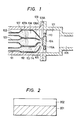
- Fig. l is a partial sectional view showing schematic construction of the main part of an example of the deposited film forming device for embodying the process of the present invention.
- l0l is a deposition chamber in which a silicon thin film is formed, and the deposition chamber l0l is internally connected to an evacuation system not shown through an evacuation outlet l06, whereby the deposition chamber l0l can be internally maintained at a desired pressure.
- the deposition chamber l0l there are a set of an introducing pipe l02 for the radical containing Si and halogen which is the activated species (A) and an introducing pipe l03 for hydrogen radicals which is the activated species (B).
- the tips of the respective radical introducing pipes are thick at the acting chambers l08, l08A and narrowed at the outlets l09, l09A.
- a substrate supporting member l04 is held so as to be reciprocally movable in the direction perpendicular to the paper surface by the roller ll0. And on the supporting member l04 is held a substrate l05 for deposition.
- the respective radicals coming out from the outlets l09, l09A are mixed and react with each other in the vicinity of the substrate within the deposition chamber l0l to form a film on the substrate.
- the radicals containing silicon and halogen and hydrogen radicals are formed from the respective starting material gases in the radical forming sections such as heating furnaces of plasma chambers, etc. (not shown) respectively, and thereafter introduced through the introducing pipes l02, l03, respectively into the acting chambers l08, l08A. Their amounts are controlled by massflow controllers on the gas source said from the heating furnace or plasma chamber.
- Roller ll0 is provided for depositing a silicon thin film over the whole surface of the substrate by moving the substrate l05.
- the introducing pipe lll is an introducing pipe for another gas having chemical or physical etching activity, and in some cases the gas is excited in the heating furnace or plasma furnace (not shown) and led to the outlet ll4. From the outlet ll4, the gas having etching activity for attacking the film is released to cut and exclude selectively bonds other than the bonds in the prescribed growth direction of the film.
- Introduction of the etching active gas, other than through such separate introduction pipes, can be also done through the introduction pipes l02, l03, mixed with starting gases, when the reactivity with the starting gas is low.
- a deposited film of the present invention it is possible to increase the crystal grain size of polycrystal and in its turn to convert it to single crystal by irradiation of an electromagnetic wave such as light or microwave, etc., or electron beam which is a film heating means, or application of heat onto the deposited film at the early stage of the film forming step or during film formation or after film formation.
- an electromagnetic wave such as light or microwave, etc., or electron beam which is a film heating means, or application of heat onto the deposited film at the early stage of the film forming step or during film formation or after film formation.
- the above treatment is effected at the early stage of the film formation step it is preferred to effect it at the state of an extremely thin film of 2000 ⁇ or less, desirably l000 ⁇ or less.
- film formation is once intermitted when a film of 2000 ⁇ or less, desirably l000 ⁇ or less has been formed, and the grain size of the crystal is enlarged or the polycrystal is converted to single crystal by irradiation of an electromagnetic wave such as light or microwave or electron beam or application of heat to prepare a base film with regular oriented faces.
- “during film formation” refers to irradiation of an electromagnetic wave such as light or microwave or electron beam or application of heat simultaneously with film formation, and by subjecting only the surface layer of the deposited film to the above treatment, formation of a deposited film with enlarged crystal grain size or a single-crystallized deposited film rendered possible at lower energy than in the prior art. Accordingly, the amount of heat generated is small, and also the damages given to the base plate, etc., and diffusion of impurities are also small, whereby the surface can be made flat.
- the grain size of crystal is enlarged and the dangling bonds at the crystal grain boundary are effectively terminated with atoms of halogen or hydrogen, whereby the electrical characteristic at the crystal grain boundary can be improved to result in improvement of electrical characteristic of the film as a whole.
- the treatment "after the deposition” as described above refers to the time point after completion of film formation, and by irradiation of an electromagnetic wave such as light or microwave or electron beam or application of heat at that point, enlargement of the grain size of crystal or single-crystallization can be effected.
- the etching effect on the growth surface of the deposited film can be aided by photoenergy irradiation which gives rise to etching selectivity. That is, the substance (E) for etching is optically excited to increase etching activity, which can make crystal growth in a specific direction more efficient.
- This photoenergy irradiation should preferably be selected so as to act more efficiently on the substance (E) for etching than on the starting gas for film formation.
- Fig. 9 is a schematic constitutional view of an example of the device for forming a deposited film for embodying the process of the present invention when photoenergy is subsidiarilly used.
- 90l is a deposition chamber in which formation of a deposited film such as a polycrystalline silicon film or the like is effected, and the deposition chamber 90l is internally connected to an evacuation system (not shown) through an evacuation pipe 92l, whereby the deposition chamber l0l can be internally held at a desired pressure through an evacuation valve 920.
- the pressure in the deposition chamber 90l is controlled to ordinarily at l0 Torr to l.0 Torr, preferably at l0 ⁇ 4 Torr to 0.l Torr.
- a desired substrate 903 is placed on the substrate supporting stand 902.
- the 904 is a heater for heating the substrate, and electricity is supplied through a conductive wire 905 to generate heat.
- the substrate temperature is not particularly limited, but it should preferably be l00 to 500 °C, more preferably l50 to 400 °C, in practicing the process of the present invention.
- gas feeding sources 906 through 9ll are gas feeding sources, and provided corresponding to the number of silicon compounds and hydrogen, halogen compound, inert gases, compounds containing impurity elements as the component which may be optionally employed.
- an appropriate gasifying is provided.
- the symbols of the gas feeding sources 906 through 9ll at fixed with a show branched pipes, those affixed with b are flow meters, those affixed with c are pressure gauges for measuring the pressures on the higher pressure side, those affixed with d or e are valves for controlling the respective gas flow rates.
- 9l2, 925, 926 are gas introducing pipes into the film forming space.
- 9l7 is a photoenergy generating device, and for example, mercury lamp, xenon lamp, carbon dioxide laser, argon ion laser, excimer laser, etc., may be employed.
- the light 9l8 directed from the photoenergy generating device 9l7 by use of a suitable optical system toward the whole of the substrate or a desired portion of the substrate is irradiated on the starting gas, etc., flowing in the direction of the arrowhead 9l9 to excite the gases, etc., of the film forming starting material and effect the reaction, thereby forming a deposited film of Si on the whole or a desired portion of the substrate 903.
- 9l4 and 923 are activation spaces for forming activated species (A) and activated species (B), respectively, and 9l3, 922 are each microwave plasma generating device for formation of activated species.
- the photoenergy is imparted uniformly or selectively controllably to the gaseous substance (E) or decomposed product which have reached in the vicinity of the substrate for film formation
- use of photoenergy has conveniences such that a deposited film can be formed by irradiating the whole of a substrate by use of a suitable optical system, or that a deposited film can be formed partially only at a desired portion by selective and controlled irradiation.
- a deposited film can be formed by irradiation of only a desired pattern portion by use of a resist, etc., and therefore it can be advantageously used.
- a silicon thin film was formed on a substrate of a flat plate glass substrate (#7059), produced by Corning Co.) by means of the device shown in Fig. l.
- SiF4 gas as the starting gas for formation of radicals containing silicon and halogen, this was permitted to flow into the reaction furnace maintained at ll00°C to be decomposed, followed by release through the introducing pipe l02 into the acting chamber l08.
- H2 gas was permitted to flow into the introducing pipe l03 and a microwave of 2.45 GHz was introduced at a power of 0.5W/cm2 into said introducing pipe 3 to effect discharging to decompose H2, followed by release into the acting chamber l08.
- the substrate temperature was maintained at 250°C
- the film becomes amorphous.
- the grain size was measured according to the Debye-Scherrar method and by use of a transmission electron microscope.
- Example l By means of the same device as used in Example l, a film was deposited on a flat plate Corning #7059 base plate as the substrate by introducing excited species of Si2F6 as the source into the introducing pipe l02 and introducing excited species of H2 into the introducing pipe l03.
- Si2F6 as the starting gas for formation of radicals containing silicon and halogen, this was permitted to flow into the reaction furnace maintained at 800 °C to be decomposed, followed by release from the introducing pipe l02 into the acting chamber l08. At the same time, F2 was permitted to flow through the introducing pipe lll, and discharging was effected by introducing microwave of 2.45 GHz at a power of 0.7 W/cm2, and the discharged product was released into the acting chamber ll3.
- the flow rate ratios of the respective starting gases were changed as 5/l00, l5/l00 25/l00, 35/l00, 50/l00 of H2 gas flow rate/Si2F6 decomposed gas (unit is SCCM), with H2 being made constant 30 SCCM, and a pressure of 0.5 Torr was maintained for l hour under the respective conditions, whereby the films having the properties as shown in Table 2A were deposited.
- Nos. A-8 and A-9 drift mobility was measured, and a high value of 40.l5 cm2/V sec was obtained for each sample. Thus, it has been found that good film was deposited.
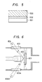
- a thin film transistor (hereinafter abbreviated as TFT) as shown in Fig. 3 was prepared.
- TFT thin film transistor
- a n+ layer (specific resistivity ⁇ ⁇ l ⁇ cm) which is the ohmic contact layer 303 doped with P was deposited to a thickness of l000 ⁇ and then an active layer 302 was remained by photolithography, followed by etching of the channel portion 306 to form the above contact layer 303.
- the TFT by use of the film as obtained above was found to have good characteristics.
- a silicon thin film was formed on a substrate of a flat plate glass substrate (#7059, produced by Corning Co.) by means of the device shown in Fig. l.
- SiF4 gas as the starting gas for formation of radicals containing silicon and halogen, this was permitted to flow into the reaction furnace maintained at ll00 °C to be decomposed, followed by release through the introducing pipe l02 into the acting chamber l08.
- H2 gas was permitted flow into the introducing pipe l03 and a microwave of 2.45GHz was introduced at a power of 0.5 W/cm2 into said introducing pipe 3 to effect discharging to decompose H2, followed by release into the acting chamber l08.
- the substrate temperature was maintained at 250 °C.
- Example 2 Under the same condition as in sample No. B-3, a polycrystalline film 202(l000 ⁇ of film thickness) was formed on a glass substrate 20l.
- a polycrystalline film with the great grain size and best orientation is prepared to be subjected to the following treatment.
- the substrate sample No. B-3 was delivered from the reaction chamber 402 to the annealing chamber 403 as shown in Fig. 4, and annealing was effected at a substrate temperature of 200 °C in H2 of 0.2 Torr by use of Ar ion laser, through the quarts window 404, at an output of l W at a scanning speed of 50 cm/sec with a beam diameter on the sample of 50 ⁇ m with a pitch of scanning of 35 ⁇ m.
- the crystal grain size was enlarged from 2300 ⁇ on an average to 2 ⁇ m on an average.
- the intensity of peak at the orientation face of (2,2,0) corresponding to the face direction (l,l,0) was increased to 5-fold or more.
- a polycrystalline film 503 was deposited to 4000 ⁇ on a polycrystalline film 502 under the same condition at in the sample No. B-3 in the same Table lB as described above. Thhis is shown in Fig. 5.
- 50l and 502 correspond to 20l and 202, respectively.
- a polycrystalline film 503 with an average grain size of 3 ⁇ m was obtained.
- the film surface was flat with unevenness difference of l00 ⁇ or less, and the drift mobility was measured to be 330 cm2/v ⁇ s.
- a polycrystalline film of l000 ⁇ was deposited under entirely the same conditions as in Example 4, i.e. the same condition as in sample No. 3 in Table lB, and the sample was delivered into the annealing chamber 403, where ArF excimer laser with wavelength of l93 nm and pulse width of 30 nsec was irradiated through the quarts window 404 at 2l0 mJ/cm2 and l00 pulses onto the sample maintained at 250 °C. As the result, the grain size of the polycrystalline film was grown to l ⁇ m or more on an average.
- a halogen lamp 604 is externally arranged and the device is converted so that the light is condensed linearly with a width of l mm or less in the direction perpendicular to the moving direction by the roller on the substrate.
- a polycrystalline film was deposited under the same conditions as in sample No. B-3 in Table l3.
- the halogen lamp 604 was irradiated simultaneously with deposition and the sample was moved reciprocally by a roller at 2 mm/sec the film was formed.
- the temperature of the sample surface on which the halogen lamp light was condensed during this operation was 600 °C.
- a polycrystalline film was deposited to thickness of 5000 ⁇ .
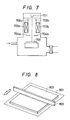
- a tungsten wire heater was arranged perpendicularly to the moving direction of the sample by the roller at a distance of 3 mm from the substrate surface.
- the wire heater was heated to 850 °C, and a polycrystalline film of 5000 ⁇ was deposited on the substrate under the same conditions as in sample No. B-3 in Table lB, while the sample was moved by the roller at l.5 mm/sec.
- the crystal grain size was 2 um on an average, the surface unevenness l00 ⁇ or less, and mobility 290 cm2/v ⁇ s.
- An electron beam narrowed to a beam current of 2 mA and a beam diameter of 100 ⁇ at acceleration voltage of 7KV was irradiated onto the sample 700 maintained at a substrate temperature of 350°C, and scanned at a scanning speed of 400 mm/sec and a line delivery pitch of 50 ⁇ in a reduced pressure of 10 ⁇ 7.
- a polycrystalline film with an average crystal grain size of 1 ⁇ m, surface unevenness of 200 ⁇ or less and mobility of l60 cm2/v ⁇ s was obtained.
- polycrystalline Si film of 5000 ⁇ was formed on a glass substrate.
- the sample 802 was placed on the heater 80l fixed at the lower portion as shown in Fig. 8 in hydrogen gas of 0.l Torr. While the heater 803 movable at the upper portion was moved at l mm/sec, heating was performed. During this operation, the heater fixed at the lower portion was maintained at 600 °C, the heater movable at the upper portion at ll00 °C. And the distance between the heater movable at the upper portion and the sample 802 surface was made 2 mm. As the result, a polycrystalline film with an average crystal grain size of l ⁇ m or more, surface unevenness of l50 ⁇ or less and mobility of l80 cm2/v ⁇ s was obtained.
- polycrystalline semiconductor Si film was grown on a glass substrate, but it is also possible to form an insulating film such as silicon nitride film, silicon oxide film by the glow discharge method, etc., and permit polycrystalline semiconductor Si film to grow on the insulating film. Also, when annealing is effected after film formation, it is also possible to perform laser annealing, electron beam annealing, etc., only on the semicnductor passage portion after formation of a device such as TFT.
- film forming conditions various annealing methods, conditions, etc., are not limited to those as shown in the above examples.
- a polycrystalline silicon film was formed on said substrate. That is, a substrate (#7059) 903 was placed on a supporting stand 902, and the deposition chamber 901 was internally evacuated by means of an evacuation device to be reduced in pressure to about 10 ⁇ 6 Torr. H2 gas was introduced from the bomb 906 for gas feeding at 50 sccm through the gas introducing pipe 925 into the activation chamber (B) 923.
- H2 gas, etc., introduced into the activation chamber (B) was activated by the microwave plasma generating device 922 to be converted to active hydrogen, etc., and the active hydrogen, etc., were introduced through the introducing pipe 924 into the film forming chamber 901.
- SiF4 gas was introduced at 20 sccm through the gas introducing pipe 512 into the activation chamber (A) 514 was activated by means of the microwave plasma generating device 513 and introduced through the introducing pipe 512 into the film forming chamber 501. Further, F2 gas was introduced as the etching gas at 10 sccm through the gas introducing pipe 526 into the film forming chamber 501.
- the light from the 1KW Xe lamp was irradiated vertically onto the substrate 503 previously heated to 350°C by the heater 104 to deposit a polycrystalline silicon film by effecting mutual chemical reaction of the activated species, and at the same time form F* by activation of F2 gas by the above mentioned photoirradiation, thereby effecting etching simultaneously with film formation of said polycrystalline silicon film by utilizing the difference in etching speed depending on the crystal faces, to form a polycrystalline silicon film with a strong orientation in a specific direction.
- the difference in etching speed depending on the crystal face was (1,0,0) > (1,1,1) > (1,1,0), whereby a polycrystalline silicon film having (1,1,0) face as the main crystal face was formed. That is, when the formed polycrystalline silicon film was evaluated by X-ray diffraction, the peak intensity at the crystal angle (2 ⁇ ) of 47.3 degree reflecting the (1,1,0) face exhibited a value which was 7 to 10-fold of the peak intensity at the crystal angles (20) of 28.4 degree and 69.2 degree reflecting respectively the (1,1,1) face and (1,0,0) face. Further, the crystal grain size was observed to be 1.2 ⁇ m by a transmission type electron microscope.
- the polycrystalline film sample obtained was placed in a vapor deposition tank, and after formation of a comb-type Al gap electrode (length 250 ⁇ , width 5 ml) under an vacuum degree of 10 ⁇ 5 Torr, dark current was measured at an application voltage of 10 V to determine the dark electroconductivity ⁇ d for evaluation of the polycrystalline silicon.
- Films were formed under the same conditions as in Example 10, except for introducing halogen containing gases into the film forming space under the conditions shown in Table 7C.
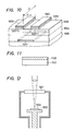
- Fig. 10 is a schematic partial perspective view showing the structure of a thin film transistor (hereinafter abbreviated as TFT) of which semiconductor part is constituted of a polycrystalline silicon formed according to the method for forming deposited film of the present invention.
- TFT thin film transistor
- a gate electrode 1001 is constituted to have a structure which is formed by laminating successively a gate electrode 1001, an electrically insulating layer 1004 so as to cover over said gate electrode 1001 on a substrate 1006 comprising glass, ceramic, etc., and a semiconductor layer 1005 comprising a polycrystalline silicon, and on the surface 1008 of the semiconductor layer 1005 are provided a first n+ layer 1007-1 and a second n+ layer 1007-2 in a juxtaposed relationship apart from each other, and further a source electrode 1002 is provided on the first n+ layer 1007-1 and a drain electrode 1003 on the second n+ layer 1007-2, respectively.
- the first n+ layer 1007-1 and the second n+ layer 1007-2 provided in contact on the surface (clean surface) 1008 on the semiconductor layer 1005 are formed after formation of the semiconductor layer 1005 without exposing said layer surface 1008 to the atmosphere or oxygen.
- the distance L between the source electrode 1002 and the drain electrode 1003 is 50 ⁇
- the length Z of the source electrode 1002 and the drain electrode 1003 is 10 mm.
- the semiconductor layer 1005 in this example was formed under the same condition as sample No. C-1 (which corresponds to C-9-1), C-2-2 (which corresponds to C-9-2).
- the TFT by use of the polycrystalline silicon film obtained as described above was found to exhibit good characteristics.
- a polycrystalline film 12 was deposited to 1000 ⁇ on the glass substrate 1101 according to the process as described above under the conditions in Table 1C.
- Xe lamp was replaced with Ar ion laser, at a substrate temperature of 200 °C by use of Ar ion laser in H2 of 0.2 Torr, through the quartz window 1201, annealing was effected at an output of 1 W with a beam diameter of 50 um at a scanning speed of 50 cm/sec and a pitch of scanning of 35 ⁇ m.
- the crystal grain size was enlarged from 2100 ⁇ on an average to 2 ⁇ m on an average.
- the intensity peak on the orientation face of (220) was found to be increased to 5-fold or more.
- a polycrystalline film 502 of 1000 ⁇ was deposited, and with removal of Xe lamp, ArF excimer laser with a wavelength of 193 nm and a pulse width of 30 nsec was irradiated on a sample maintained at 250 °C at 210 mJ/cm2 and 100 pulses.
- the grain size of the polycrystalline film was grown to 1 um or more on an average.
- a polycrystallien film with unevenness of the film surface of 80 ⁇ or less, an average grain size of 1.5 ⁇ m or more and a mobility of 180 cm2/v ⁇ s was obtained.
- Xe lamp 1301 and halogen lamp 1302 were mounted at the same time, and the halogen lamp light was condensed linearly with a width of 1 mm or less in the direction perpendicular to the moving direction by the roller on the substrate. This is shown in Fig. 13.
- a polycrystalline film was deposited under the same conditions as in Table 1C.
- the halogen lamp 1302 was irradiated simultaneously with deposition and the sample was moved by a roller at 2 mm/sec.
- the temperature of the sample surface on which the halogen lamp light was condensed during this operation was 600 °C.
- the sample was moved reciprocally by the roller to deposit a polycrystalline film of 5000 ⁇ .
- a tungsten wire heater was arranged perpendicularly to the moving direction of the sample by the roller at a distance of 3 mm from the substrate surface.
- the wire heater was heated to 850 °C, and a polycrystalline film of 5000 ⁇ was deposited under the same conditions as in Table 1C in Example 19, while the sample was moved by the roller at 1.5 mm/sec As the result, the crystal grain size was 2 um on an average, the surface unevenness 100 ⁇ or less, and mobility 290 cm2/v ⁇ s.
- a polycrystalline Si film of 5000 ⁇ was formed on a glass substrate, and then with the sampel 802 being placed on the heater 801 fixed at the lower portion as shown in Fig. 8 in hydrogen gas of 0.1 Torr, the heater 803 movable at the upper portion was moved at 1 mm/sec. During this operation, the heater fixed at the lower portion was maintained at 600 °C, the heater movable at the upper portion at 1100 °C. And the distance between the heater movable at the upper portion and the sample surface was made 2 mm. As the result, a polycrystalline film with an average crystal grain size of 1 ⁇ m or more, surface unevenness of 150 ⁇ or less and mobility of 180 cm2/v ⁇ s was obtained.
Landscapes
- Chemical & Material Sciences (AREA)
- General Chemical & Material Sciences (AREA)
- Chemical Kinetics & Catalysis (AREA)
- Engineering & Computer Science (AREA)
- Materials Engineering (AREA)
- Mechanical Engineering (AREA)
- Metallurgy (AREA)
- Organic Chemistry (AREA)
- Inorganic Chemistry (AREA)
- Chemical Vapour Deposition (AREA)
Priority Applications (1)
| Application Number | Priority Date | Filing Date | Title |
|---|---|---|---|
| AT87303225T ATE86793T1 (de) | 1986-04-11 | 1987-04-13 | Herstellungsverfahren einer niedergeschlagenen schicht. |
Applications Claiming Priority (8)
| Application Number | Priority Date | Filing Date | Title |
|---|---|---|---|
| JP61083924A JP2662388B2 (ja) | 1986-04-11 | 1986-04-11 | 堆積膜形成法 |
| JP83924/86 | 1986-04-11 | ||
| JP85507/86 | 1986-04-14 | ||
| JP8550786A JPH0639701B2 (ja) | 1986-04-14 | 1986-04-14 | 堆積膜形成法 |
| JP85508/86 | 1986-04-14 | ||
| JP8550886A JPS62240767A (ja) | 1986-04-14 | 1986-04-14 | 堆積膜形成法 |
| JP86825/86 | 1986-04-15 | ||
| JP8682586A JPS62243767A (ja) | 1986-04-15 | 1986-04-15 | 堆積膜形成法 |
Publications (3)
| Publication Number | Publication Date |
|---|---|
| EP0241317A2 true EP0241317A2 (de) | 1987-10-14 |
| EP0241317A3 EP0241317A3 (en) | 1989-02-08 |
| EP0241317B1 EP0241317B1 (de) | 1993-03-10 |
Family
ID=27466894
Family Applications (1)
| Application Number | Title | Priority Date | Filing Date |
|---|---|---|---|
| EP87303225A Expired - Lifetime EP0241317B1 (de) | 1986-04-11 | 1987-04-13 | Herstellungsverfahren einer niedergeschlagenen Schicht |
Country Status (3)
| Country | Link |
|---|---|
| US (1) | US5591492A (de) |
| EP (1) | EP0241317B1 (de) |
| DE (1) | DE3784537T2 (de) |
Cited By (7)
| Publication number | Priority date | Publication date | Assignee | Title |
|---|---|---|---|---|
| EP0343355A1 (de) * | 1988-05-26 | 1989-11-29 | Energy Conversion Devices, Inc. | Verfahren zur Erzeugung eines hohen Flusses von aktivierten Teilchen für die Reaktion mit einem entfernt angeordneten Substrat |
| AU598247B2 (en) * | 1986-04-15 | 1990-06-21 | Canon Kabushiki Kaisha | Process for forming deposited film |
| EP0359264A3 (en) * | 1988-09-14 | 1990-11-14 | Fujitsu Limited | Hydrogenated amorphous materials and thin films thereof |
| US5135607A (en) * | 1986-04-11 | 1992-08-04 | Canon Kabushiki Kaisha | Process for forming deposited film |
| EP0243074B1 (de) * | 1986-04-14 | 1993-03-10 | Canon Kabushiki Kaisha | Herstellungsverfahren einer niedergeschlagenen Schicht |
| EP0241311B1 (de) * | 1986-04-11 | 1993-03-17 | Canon Kabushiki Kaisha | Verfahren zur Herstellung einer niedergeschlagenen Schicht |
| EP0242182B1 (de) * | 1986-04-14 | 1993-06-30 | Canon Kabushiki Kaisha | Verfahren zur Herstellung einer niedergeschlagenen Schicht |
Families Citing this family (12)
| Publication number | Priority date | Publication date | Assignee | Title |
|---|---|---|---|---|
| JPH06124913A (ja) * | 1992-06-26 | 1994-05-06 | Semiconductor Energy Lab Co Ltd | レーザー処理方法 |
| JP3765902B2 (ja) * | 1997-02-19 | 2006-04-12 | 株式会社半導体エネルギー研究所 | 半導体装置の作製方法および電子デバイスの作製方法 |
| US6149829A (en) * | 1998-03-17 | 2000-11-21 | James W. Mitzel | Plasma surface treatment method and resulting device |
| NL1017849C2 (nl) * | 2001-04-16 | 2002-10-30 | Univ Eindhoven Tech | Werkwijze en inrichting voor het deponeren van een althans ten dele kristallijne siliciumlaag op een substraat. |
| US6998305B2 (en) * | 2003-01-24 | 2006-02-14 | Asm America, Inc. | Enhanced selectivity for epitaxial deposition |
| US7404858B2 (en) * | 2005-09-16 | 2008-07-29 | Mississippi State University | Method for epitaxial growth of silicon carbide |
| US8125069B2 (en) * | 2006-04-07 | 2012-02-28 | Philtech Inc. | Semiconductor device and etching apparatus |
| US20090102025A1 (en) * | 2006-04-07 | 2009-04-23 | Toshio Hayashi | Semiconductor device and method for manufacturing the same, dry-etching process, method for making electrical connections, and etching apparatus |
| US8278176B2 (en) | 2006-06-07 | 2012-10-02 | Asm America, Inc. | Selective epitaxial formation of semiconductor films |
| US7759199B2 (en) * | 2007-09-19 | 2010-07-20 | Asm America, Inc. | Stressor for engineered strain on channel |
| US8367528B2 (en) * | 2009-11-17 | 2013-02-05 | Asm America, Inc. | Cyclical epitaxial deposition and etch |
| US8809170B2 (en) | 2011-05-19 | 2014-08-19 | Asm America Inc. | High throughput cyclical epitaxial deposition and etch process |
Family Cites Families (30)
| Publication number | Priority date | Publication date | Assignee | Title |
|---|---|---|---|---|
| US3461003A (en) * | 1964-12-14 | 1969-08-12 | Motorola Inc | Method of fabricating a semiconductor structure with an electrically isolated region of semiconductor material |
| US4409605A (en) * | 1978-03-16 | 1983-10-11 | Energy Conversion Devices, Inc. | Amorphous semiconductors equivalent to crystalline semiconductors |
| US4226898A (en) * | 1978-03-16 | 1980-10-07 | Energy Conversion Devices, Inc. | Amorphous semiconductors equivalent to crystalline semiconductors produced by a glow discharge process |
| US4401687A (en) * | 1981-11-12 | 1983-08-30 | Advanced Semiconductor Materials America | Plasma deposition of silicon |
| US4422897A (en) * | 1982-05-25 | 1983-12-27 | Massachusetts Institute Of Technology | Process for selectively etching silicon |
| JPS5961124A (ja) * | 1982-09-30 | 1984-04-07 | Fujitsu Ltd | 薄膜形成方法 |
| US4521447A (en) * | 1982-10-18 | 1985-06-04 | Sovonics Solar Systems | Method and apparatus for making layered amorphous semiconductor alloys using microwave energy |
| JPS59142839A (ja) * | 1983-02-01 | 1984-08-16 | Canon Inc | 気相法装置のクリ−ニング方法 |
| JPS59207631A (ja) * | 1983-05-11 | 1984-11-24 | Semiconductor Res Found | 光化学を用いたドライプロセス装置 |
| JPH0622212B2 (ja) * | 1983-05-31 | 1994-03-23 | 株式会社東芝 | ドライエッチング方法 |
| US4522662A (en) * | 1983-08-12 | 1985-06-11 | Hewlett-Packard Company | CVD lateral epitaxial growth of silicon over insulators |
| DE3429899A1 (de) * | 1983-08-16 | 1985-03-07 | Canon K.K., Tokio/Tokyo | Verfahren zur bildung eines abscheidungsfilms |
| JPS6058616A (ja) * | 1983-09-12 | 1985-04-04 | Matsushita Electronics Corp | 薄膜の成長方法 |
| JPS60152023A (ja) * | 1984-01-20 | 1985-08-10 | Hitachi Ltd | 光cvd装置 |
| US4578142A (en) * | 1984-05-10 | 1986-03-25 | Rca Corporation | Method for growing monocrystalline silicon through mask layer |
| JPS6126774A (ja) * | 1984-07-16 | 1986-02-06 | Canon Inc | 非晶質シリコン膜形成装置 |
| US4657777A (en) * | 1984-12-17 | 1987-04-14 | Canon Kabushiki Kaisha | Formation of deposited film |
| US4615765A (en) * | 1985-02-01 | 1986-10-07 | General Electric Company | Self-registered, thermal processing technique using a pulsed heat source |
| US4717585A (en) * | 1985-02-09 | 1988-01-05 | Canon Kabushiki Kaisha | Process for forming deposited film |
| US4728528A (en) * | 1985-02-18 | 1988-03-01 | Canon Kabushiki Kaisha | Process for forming deposited film |
| JPS61189626A (ja) * | 1985-02-18 | 1986-08-23 | Canon Inc | 堆積膜形成法 |
| US4726963A (en) * | 1985-02-19 | 1988-02-23 | Canon Kabushiki Kaisha | Process for forming deposited film |
| US4778692A (en) * | 1985-02-20 | 1988-10-18 | Canon Kabushiki Kaisha | Process for forming deposited film |
| US4637895A (en) * | 1985-04-01 | 1987-01-20 | Energy Conversion Devices, Inc. | Gas mixtures for the vapor deposition of semiconductor material |
| JPS62228471A (ja) * | 1986-03-31 | 1987-10-07 | Canon Inc | 堆積膜形成法 |
| AU606053B2 (en) * | 1986-04-11 | 1991-01-31 | Canon Kabushiki Kaisha | Process for forming deposited film |
| JPH0639702B2 (ja) * | 1986-04-14 | 1994-05-25 | キヤノン株式会社 | 堆積膜形成法 |
| EP0242182B1 (de) * | 1986-04-14 | 1993-06-30 | Canon Kabushiki Kaisha | Verfahren zur Herstellung einer niedergeschlagenen Schicht |
| US4918028A (en) * | 1986-04-14 | 1990-04-17 | Canon Kabushiki Kaisha | Process for photo-assisted epitaxial growth using remote plasma with in-situ etching |
| JPH0639703B2 (ja) * | 1986-04-15 | 1994-05-25 | キヤノン株式会社 | 堆積膜形成法 |
-
1987
- 1987-04-13 DE DE87303225T patent/DE3784537T2/de not_active Expired - Fee Related
- 1987-04-13 EP EP87303225A patent/EP0241317B1/de not_active Expired - Lifetime
-
1995
- 1995-02-28 US US08/396,065 patent/US5591492A/en not_active Expired - Fee Related
Cited By (11)
| Publication number | Priority date | Publication date | Assignee | Title |
|---|---|---|---|---|
| US5135607A (en) * | 1986-04-11 | 1992-08-04 | Canon Kabushiki Kaisha | Process for forming deposited film |
| EP0241311B1 (de) * | 1986-04-11 | 1993-03-17 | Canon Kabushiki Kaisha | Verfahren zur Herstellung einer niedergeschlagenen Schicht |
| EP0243074B1 (de) * | 1986-04-14 | 1993-03-10 | Canon Kabushiki Kaisha | Herstellungsverfahren einer niedergeschlagenen Schicht |
| EP0242182B1 (de) * | 1986-04-14 | 1993-06-30 | Canon Kabushiki Kaisha | Verfahren zur Herstellung einer niedergeschlagenen Schicht |
| AU598247B2 (en) * | 1986-04-15 | 1990-06-21 | Canon Kabushiki Kaisha | Process for forming deposited film |
| EP0242207B1 (de) * | 1986-04-15 | 1993-03-10 | Canon Kabushiki Kaisha | Verfahren zur Herstellung einer niedergeschlagenen Schicht |
| EP0343355A1 (de) * | 1988-05-26 | 1989-11-29 | Energy Conversion Devices, Inc. | Verfahren zur Erzeugung eines hohen Flusses von aktivierten Teilchen für die Reaktion mit einem entfernt angeordneten Substrat |
| EP0359264A3 (en) * | 1988-09-14 | 1990-11-14 | Fujitsu Limited | Hydrogenated amorphous materials and thin films thereof |
| US5447816A (en) * | 1988-09-14 | 1995-09-05 | Fujitsu Limited | Method for forming a thin protection film |
| US5522343A (en) * | 1988-09-14 | 1996-06-04 | Fujitsu Limited | Thin film formation apparatus |
| US5741364A (en) * | 1988-09-14 | 1998-04-21 | Fujitsu Limited | Thin film formation apparatus |
Also Published As
| Publication number | Publication date |
|---|---|
| DE3784537T2 (de) | 1993-09-30 |
| EP0241317B1 (de) | 1993-03-10 |
| US5591492A (en) | 1997-01-07 |
| EP0241317A3 (en) | 1989-02-08 |
| DE3784537D1 (de) | 1993-04-15 |
Similar Documents
| Publication | Publication Date | Title |
|---|---|---|
| EP0241317A2 (de) | Herstellungsverfahren einer niedergeschlagenen Schicht | |
| US5192717A (en) | Process for the formation of a polycrystalline semiconductor film by microwave plasma chemical vapor deposition method | |
| US5246886A (en) | Process for depositing a silicon-containing polycrystalline film on a substrate by way of growing Ge-crystalline nucleus | |
| EP0230788A1 (de) | Verfahren zur Herstellung eines vielschichtigen strukturierten Films | |
| JP2566914B2 (ja) | 薄膜半導体素子及びその形成法 | |
| US4683144A (en) | Method for forming a deposited film | |
| US4918028A (en) | Process for photo-assisted epitaxial growth using remote plasma with in-situ etching | |
| US4942058A (en) | Process for forming deposited film | |
| US4800173A (en) | Process for preparing Si or Ge epitaxial film using fluorine oxidant | |
| US5294285A (en) | Process for the production of functional crystalline film | |
| US5135607A (en) | Process for forming deposited film | |
| EP0240306B1 (de) | Verfahren zur Bildung eines abgeschiedenen Filmes | |
| EP0242182B1 (de) | Verfahren zur Herstellung einer niedergeschlagenen Schicht | |
| EP0241311B1 (de) | Verfahren zur Herstellung einer niedergeschlagenen Schicht | |
| EP0243074B1 (de) | Herstellungsverfahren einer niedergeschlagenen Schicht | |
| JPH0682616B2 (ja) | 堆積膜形成方法 | |
| JP2547740B2 (ja) | 堆積膜形成法 | |
| JP3126176B2 (ja) | 半導体薄膜 | |
| JP2662388B2 (ja) | 堆積膜形成法 | |
| JP3040247B2 (ja) | シリコン薄膜の製造法 | |
| JPH0590157A (ja) | n型半導体薄膜 | |
| JPS62243767A (ja) | 堆積膜形成法 | |
| JPH01730A (ja) | 多層薄膜の形成方法 | |
| JPS62243766A (ja) | 堆積膜形成法 | |
| Bruno et al. | ISPC-7 Eindhoven, July 1985 |
Legal Events
| Date | Code | Title | Description |
|---|---|---|---|
| PUAI | Public reference made under article 153(3) epc to a published international application that has entered the european phase |
Free format text: ORIGINAL CODE: 0009012 |
|
| AK | Designated contracting states |
Kind code of ref document: A2 Designated state(s): AT BE CH DE ES FR GB GR IT LI LU NL SE |
|
| PUAL | Search report despatched |
Free format text: ORIGINAL CODE: 0009013 |
|
| AK | Designated contracting states |
Kind code of ref document: A3 Designated state(s): AT BE CH DE ES FR GB GR IT LI LU NL SE |
|
| 17P | Request for examination filed |
Effective date: 19890705 |
|
| 17Q | First examination report despatched |
Effective date: 19900817 |
|
| GRAA | (expected) grant |
Free format text: ORIGINAL CODE: 0009210 |
|
| AK | Designated contracting states |
Kind code of ref document: B1 Designated state(s): AT BE CH DE ES FR GB GR IT LI LU NL SE |
|
| PG25 | Lapsed in a contracting state [announced via postgrant information from national office to epo] |
Ref country code: NL Effective date: 19930310 Ref country code: GR Free format text: LAPSE BECAUSE OF FAILURE TO SUBMIT A TRANSLATION OF THE DESCRIPTION OR TO PAY THE FEE WITHIN THE PRESCRIBED TIME-LIMIT Effective date: 19930310 Ref country code: BE Effective date: 19930310 Ref country code: AT Effective date: 19930310 |
|
| REF | Corresponds to: |
Ref document number: 86793 Country of ref document: AT Date of ref document: 19930315 Kind code of ref document: T |
|
| REF | Corresponds to: |
Ref document number: 3784537 Country of ref document: DE Date of ref document: 19930415 |
|
| PG25 | Lapsed in a contracting state [announced via postgrant information from national office to epo] |
Ref country code: LU Free format text: LAPSE BECAUSE OF NON-PAYMENT OF DUE FEES Effective date: 19930430 |
|
| ET | Fr: translation filed | ||
| ITF | It: translation for a ep patent filed | ||
| PG25 | Lapsed in a contracting state [announced via postgrant information from national office to epo] |
Ref country code: ES Free format text: LAPSE BECAUSE OF FAILURE TO SUBMIT A TRANSLATION OF THE DESCRIPTION OR TO PAY THE FEE WITHIN THE PRESCRIBED TIME-LIMIT Effective date: 19930621 |
|
| NLV1 | Nl: lapsed or annulled due to failure to fulfill the requirements of art. 29p and 29m of the patents act | ||
| PLBE | No opposition filed within time limit |
Free format text: ORIGINAL CODE: 0009261 |
|
| STAA | Information on the status of an ep patent application or granted ep patent |
Free format text: STATUS: NO OPPOSITION FILED WITHIN TIME LIMIT |
|
| 26N | No opposition filed | ||
| ITTA | It: last paid annual fee | ||
| EAL | Se: european patent in force in sweden |
Ref document number: 87303225.4 |
|
| REG | Reference to a national code |
Ref country code: GB Ref legal event code: IF02 |
|
| PGFP | Annual fee paid to national office [announced via postgrant information from national office to epo] |
Ref country code: GB Payment date: 20020402 Year of fee payment: 16 |
|
| PGFP | Annual fee paid to national office [announced via postgrant information from national office to epo] |
Ref country code: CH Payment date: 20020415 Year of fee payment: 16 |
|
| PGFP | Annual fee paid to national office [announced via postgrant information from national office to epo] |
Ref country code: SE Payment date: 20020422 Year of fee payment: 16 |
|
| PGFP | Annual fee paid to national office [announced via postgrant information from national office to epo] |
Ref country code: DE Payment date: 20020423 Year of fee payment: 16 |
|
| PGFP | Annual fee paid to national office [announced via postgrant information from national office to epo] |
Ref country code: FR Payment date: 20020429 Year of fee payment: 16 |
|
| PG25 | Lapsed in a contracting state [announced via postgrant information from national office to epo] |
Ref country code: GB Free format text: LAPSE BECAUSE OF NON-PAYMENT OF DUE FEES Effective date: 20030413 |
|
| PG25 | Lapsed in a contracting state [announced via postgrant information from national office to epo] |
Ref country code: SE Free format text: LAPSE BECAUSE OF NON-PAYMENT OF DUE FEES Effective date: 20030414 |
|
| PG25 | Lapsed in a contracting state [announced via postgrant information from national office to epo] |
Ref country code: LI Free format text: LAPSE BECAUSE OF NON-PAYMENT OF DUE FEES Effective date: 20030430 Ref country code: CH Free format text: LAPSE BECAUSE OF NON-PAYMENT OF DUE FEES Effective date: 20030430 |
|
| PG25 | Lapsed in a contracting state [announced via postgrant information from national office to epo] |
Ref country code: DE Free format text: LAPSE BECAUSE OF NON-PAYMENT OF DUE FEES Effective date: 20031101 |
|
| EUG | Se: european patent has lapsed | ||
| GBPC | Gb: european patent ceased through non-payment of renewal fee |
Effective date: 20030413 |
|
| REG | Reference to a national code |
Ref country code: CH Ref legal event code: PL |
|
| PG25 | Lapsed in a contracting state [announced via postgrant information from national office to epo] |
Ref country code: FR Free format text: LAPSE BECAUSE OF NON-PAYMENT OF DUE FEES Effective date: 20031231 |
|
| REG | Reference to a national code |
Ref country code: FR Ref legal event code: ST |
|
| PG25 | Lapsed in a contracting state [announced via postgrant information from national office to epo] |
Ref country code: IT Free format text: LAPSE BECAUSE OF NON-PAYMENT OF DUE FEES;WARNING: LAPSES OF ITALIAN PATENTS WITH EFFECTIVE DATE BEFORE 2007 MAY HAVE OCCURRED AT ANY TIME BEFORE 2007. THE CORRECT EFFECTIVE DATE MAY BE DIFFERENT FROM THE ONE RECORDED. Effective date: 20050413 |