EP0226218A2 - Flüssigkristallvorrichtung - Google Patents
Flüssigkristallvorrichtung Download PDFInfo
- Publication number
- EP0226218A2 EP0226218A2 EP86117613A EP86117613A EP0226218A2 EP 0226218 A2 EP0226218 A2 EP 0226218A2 EP 86117613 A EP86117613 A EP 86117613A EP 86117613 A EP86117613 A EP 86117613A EP 0226218 A2 EP0226218 A2 EP 0226218A2
- Authority
- EP
- European Patent Office
- Prior art keywords
- liquid crystal
- crystal device
- color filter
- protection layer
- filter layer
- Prior art date
- Legal status (The legal status is an assumption and is not a legal conclusion. Google has not performed a legal analysis and makes no representation as to the accuracy of the status listed.)
- Granted
Links
Images


Classifications
-
- G—PHYSICS
- G02—OPTICS
- G02F—OPTICAL DEVICES OR ARRANGEMENTS FOR THE CONTROL OF LIGHT BY MODIFICATION OF THE OPTICAL PROPERTIES OF THE MEDIA OF THE ELEMENTS INVOLVED THEREIN; NON-LINEAR OPTICS; FREQUENCY-CHANGING OF LIGHT; OPTICAL LOGIC ELEMENTS; OPTICAL ANALOGUE/DIGITAL CONVERTERS
- G02F1/00—Devices or arrangements for the control of the intensity, colour, phase, polarisation or direction of light arriving from an independent light source, e.g. switching, gating or modulating; Non-linear optics
- G02F1/01—Devices or arrangements for the control of the intensity, colour, phase, polarisation or direction of light arriving from an independent light source, e.g. switching, gating or modulating; Non-linear optics for the control of the intensity, phase, polarisation or colour
- G02F1/13—Devices or arrangements for the control of the intensity, colour, phase, polarisation or direction of light arriving from an independent light source, e.g. switching, gating or modulating; Non-linear optics for the control of the intensity, phase, polarisation or colour based on liquid crystals, e.g. single liquid crystal display cells
- G02F1/133—Constructional arrangements; Operation of liquid crystal cells; Circuit arrangements
- G02F1/1333—Constructional arrangements; Manufacturing methods
- G02F1/1335—Structural association of cells with optical devices, e.g. polarisers or reflectors
- G02F1/133509—Filters, e.g. light shielding masks
- G02F1/133514—Colour filters
-
- G—PHYSICS
- G02—OPTICS
- G02F—OPTICAL DEVICES OR ARRANGEMENTS FOR THE CONTROL OF LIGHT BY MODIFICATION OF THE OPTICAL PROPERTIES OF THE MEDIA OF THE ELEMENTS INVOLVED THEREIN; NON-LINEAR OPTICS; FREQUENCY-CHANGING OF LIGHT; OPTICAL LOGIC ELEMENTS; OPTICAL ANALOGUE/DIGITAL CONVERTERS
- G02F1/00—Devices or arrangements for the control of the intensity, colour, phase, polarisation or direction of light arriving from an independent light source, e.g. switching, gating or modulating; Non-linear optics
- G02F1/01—Devices or arrangements for the control of the intensity, colour, phase, polarisation or direction of light arriving from an independent light source, e.g. switching, gating or modulating; Non-linear optics for the control of the intensity, phase, polarisation or colour
- G02F1/13—Devices or arrangements for the control of the intensity, colour, phase, polarisation or direction of light arriving from an independent light source, e.g. switching, gating or modulating; Non-linear optics for the control of the intensity, phase, polarisation or colour based on liquid crystals, e.g. single liquid crystal display cells
- G02F1/133—Constructional arrangements; Operation of liquid crystal cells; Circuit arrangements
- G02F1/1333—Constructional arrangements; Manufacturing methods
- G02F1/133345—Insulating layers
-
- G—PHYSICS
- G02—OPTICS
- G02F—OPTICAL DEVICES OR ARRANGEMENTS FOR THE CONTROL OF LIGHT BY MODIFICATION OF THE OPTICAL PROPERTIES OF THE MEDIA OF THE ELEMENTS INVOLVED THEREIN; NON-LINEAR OPTICS; FREQUENCY-CHANGING OF LIGHT; OPTICAL LOGIC ELEMENTS; OPTICAL ANALOGUE/DIGITAL CONVERTERS
- G02F1/00—Devices or arrangements for the control of the intensity, colour, phase, polarisation or direction of light arriving from an independent light source, e.g. switching, gating or modulating; Non-linear optics
- G02F1/01—Devices or arrangements for the control of the intensity, colour, phase, polarisation or direction of light arriving from an independent light source, e.g. switching, gating or modulating; Non-linear optics for the control of the intensity, phase, polarisation or colour
- G02F1/13—Devices or arrangements for the control of the intensity, colour, phase, polarisation or direction of light arriving from an independent light source, e.g. switching, gating or modulating; Non-linear optics for the control of the intensity, phase, polarisation or colour based on liquid crystals, e.g. single liquid crystal display cells
- G02F1/133—Constructional arrangements; Operation of liquid crystal cells; Circuit arrangements
- G02F1/1333—Constructional arrangements; Manufacturing methods
- G02F1/1335—Structural association of cells with optical devices, e.g. polarisers or reflectors
- G02F1/133509—Filters, e.g. light shielding masks
- G02F1/133514—Colour filters
- G02F1/133519—Overcoatings
-
- G—PHYSICS
- G02—OPTICS
- G02F—OPTICAL DEVICES OR ARRANGEMENTS FOR THE CONTROL OF LIGHT BY MODIFICATION OF THE OPTICAL PROPERTIES OF THE MEDIA OF THE ELEMENTS INVOLVED THEREIN; NON-LINEAR OPTICS; FREQUENCY-CHANGING OF LIGHT; OPTICAL LOGIC ELEMENTS; OPTICAL ANALOGUE/DIGITAL CONVERTERS
- G02F1/00—Devices or arrangements for the control of the intensity, colour, phase, polarisation or direction of light arriving from an independent light source, e.g. switching, gating or modulating; Non-linear optics
- G02F1/01—Devices or arrangements for the control of the intensity, colour, phase, polarisation or direction of light arriving from an independent light source, e.g. switching, gating or modulating; Non-linear optics for the control of the intensity, phase, polarisation or colour
- G02F1/13—Devices or arrangements for the control of the intensity, colour, phase, polarisation or direction of light arriving from an independent light source, e.g. switching, gating or modulating; Non-linear optics for the control of the intensity, phase, polarisation or colour based on liquid crystals, e.g. single liquid crystal display cells
- G02F1/133—Constructional arrangements; Operation of liquid crystal cells; Circuit arrangements
- G02F1/1333—Constructional arrangements; Manufacturing methods
- G02F1/1337—Surface-induced orientation of the liquid crystal molecules, e.g. by alignment layers
-
- G—PHYSICS
- G02—OPTICS
- G02F—OPTICAL DEVICES OR ARRANGEMENTS FOR THE CONTROL OF LIGHT BY MODIFICATION OF THE OPTICAL PROPERTIES OF THE MEDIA OF THE ELEMENTS INVOLVED THEREIN; NON-LINEAR OPTICS; FREQUENCY-CHANGING OF LIGHT; OPTICAL LOGIC ELEMENTS; OPTICAL ANALOGUE/DIGITAL CONVERTERS
- G02F1/00—Devices or arrangements for the control of the intensity, colour, phase, polarisation or direction of light arriving from an independent light source, e.g. switching, gating or modulating; Non-linear optics
- G02F1/01—Devices or arrangements for the control of the intensity, colour, phase, polarisation or direction of light arriving from an independent light source, e.g. switching, gating or modulating; Non-linear optics for the control of the intensity, phase, polarisation or colour
- G02F1/13—Devices or arrangements for the control of the intensity, colour, phase, polarisation or direction of light arriving from an independent light source, e.g. switching, gating or modulating; Non-linear optics for the control of the intensity, phase, polarisation or colour based on liquid crystals, e.g. single liquid crystal display cells
- G02F1/137—Devices or arrangements for the control of the intensity, colour, phase, polarisation or direction of light arriving from an independent light source, e.g. switching, gating or modulating; Non-linear optics for the control of the intensity, phase, polarisation or colour based on liquid crystals, e.g. single liquid crystal display cells characterised by the electro-optical or magneto-optical effect, e.g. field-induced phase transition, orientation effect, guest-host interaction or dynamic scattering
- G02F1/139—Devices or arrangements for the control of the intensity, colour, phase, polarisation or direction of light arriving from an independent light source, e.g. switching, gating or modulating; Non-linear optics for the control of the intensity, phase, polarisation or colour based on liquid crystals, e.g. single liquid crystal display cells characterised by the electro-optical or magneto-optical effect, e.g. field-induced phase transition, orientation effect, guest-host interaction or dynamic scattering based on orientation effects in which the liquid crystal remains transparent
- G02F1/141—Devices or arrangements for the control of the intensity, colour, phase, polarisation or direction of light arriving from an independent light source, e.g. switching, gating or modulating; Non-linear optics for the control of the intensity, phase, polarisation or colour based on liquid crystals, e.g. single liquid crystal display cells characterised by the electro-optical or magneto-optical effect, e.g. field-induced phase transition, orientation effect, guest-host interaction or dynamic scattering based on orientation effects in which the liquid crystal remains transparent using ferroelectric liquid crystals
-
- G—PHYSICS
- G02—OPTICS
- G02F—OPTICAL DEVICES OR ARRANGEMENTS FOR THE CONTROL OF LIGHT BY MODIFICATION OF THE OPTICAL PROPERTIES OF THE MEDIA OF THE ELEMENTS INVOLVED THEREIN; NON-LINEAR OPTICS; FREQUENCY-CHANGING OF LIGHT; OPTICAL LOGIC ELEMENTS; OPTICAL ANALOGUE/DIGITAL CONVERTERS
- G02F1/00—Devices or arrangements for the control of the intensity, colour, phase, polarisation or direction of light arriving from an independent light source, e.g. switching, gating or modulating; Non-linear optics
- G02F1/01—Devices or arrangements for the control of the intensity, colour, phase, polarisation or direction of light arriving from an independent light source, e.g. switching, gating or modulating; Non-linear optics for the control of the intensity, phase, polarisation or colour
- G02F1/15—Devices or arrangements for the control of the intensity, colour, phase, polarisation or direction of light arriving from an independent light source, e.g. switching, gating or modulating; Non-linear optics for the control of the intensity, phase, polarisation or colour based on an electrochromic effect
- G02F1/153—Constructional details
- G02F1/1533—Constructional details structural features not otherwise provided for
- G02F2001/1536—Constructional details structural features not otherwise provided for additional, e.g. protective, layer inside the cell
Definitions
- the present invention relates to a ferroelectric liquid crystal device adapted to a color display, particularly a color television panel.
- TFTs thin film transistors
- a gate-on pulse is applied to a TFT to turn on the source-drain channel
- a picture image signal is applied to the source and stored in a capacitor.
- a liquid crystal e.g., TN (twisted nematic) liquid crystal
- a color display is effected by switching the pixels each provided with a color filter layer.
- Such a television display panel of the active matrix driving system using a TN liquid crystal uses complicated structure of TFTs requiring a large number of production steps and is accompanied with a difficulty of high production cost.
- semiconductor film e.g., of polysilicon, amorphous silicon
- a display panel of a passive matrix driving type using a TN liquid crystal has been known as one of a low production cost.
- N the number of scanning lines
- a time period (duty factor) during which one selected point is subjected to an effective electric field during the time when one frame is scanned is decreased at a ratio of 1/N, whereby crosstalk occurs and a picture with a high contrast cannot be obtained.
- the duty factor is decreased, it is difficult to control gradation of respective pixels by means of voltage modulation so that this type of display is not adapted for a display panel of a high pixel or wiring density, particularly one for a liquid crystal television panel.
- ferroelectric liquid crystal devices As disclosed by, for example, U.S. Patent No. 4767924 to Clark and Lagerwall.
- a most convenient color display system using a liquid crystal device is one wherein respective color units of a color stripe filter or a color mosaic filter are optically switched or shuttered by driving a liquid crystal, especially one wherein color pixel units formed by arranging respective intersections of matrix electrodes corresponding to color units are switched line-sequentially.
- a principal object of the present invention is to provide a ferroelectric liquid crystal device capable of stably effecting a color display, particularly a color television display, for a long period of time.
- a liquid crystal device comprising a pair of substrates and a ferroelectric liquid crystal disposed between the pair of substrates, at least one of the pair of substrates having thereon a color filter layer and a protection layer for preventing direct contact between the color filter layer and the ferroelectric liquid crystal.
- a color filter is disposed inside the cell, and a dye in the color filter layer can be eluted in the ferroelectric liquid crystal within the cell, so that there arises a problem that when such a ferroelectric liquid crystal device is used for a long period of time, the resistance of the FLC is decreased with the elapse of time, until the above mentioned reverse polarity of voltage - ⁇ V0 exceeds the switching threshold voltage to fail to effect desired optical switching operation.
- application of a line-sequential writing scheme to an FLC may be effected by applying in a first phase t1 a pulse for providing a first display state based on a first orientation state of the FLC to all or a part of the pixels on a line, and applying in a second phase t2 a pulse for switching the first display state to a second display state based on a second orientation state of the FLC to a selected pixel.
- a pulse of a polarity opposite to that of the pulse applied in the phase t1 and having a voltage below the threshold voltage is applied to a picture element which is to retain the first display state as shown in Figure 2A.
- a certain pixel is required to retain the first display state, which has resulted in the phase t1, in the phase t2. Accordingly, a voltage exceeding the threshold voltage should not be applied to the pixel.
- a voltage of -(aV0+ ⁇ V0) ( a is a parameter satisfying a ⁇
- the dye in the color filter layer is prevented from being eluted or dissolved into the FLC so as to avoid the increase in reverse electric field (- ⁇ V0) caused by the decrease in resistance of the FLC.
- Figure 3 is a sectional view of a liquid crystal device according to the present invention, comprising a color filter layer which in turn comprises a blue color filter layer 31(B), a green color filter layer 31(G) and a red color filter layer 31(R), each constituting one color pixel.
- a protection layer 32 for preventing direct contact between the color filter layer 31 and an FLC 35 is disposed.
- the protection layer 32 can also be provided with an insulating property and an alignment control property.
- Reference numerals 33a and 33b denote substrates comprising, e.g., a glass plate or a plastic film, on which stripe-form transparent electrodes 34a and 34b constituting matrix electrodes of ITO (indium-tin-oxide), etc., are provided.
- a layer 36 is an alignment control film and can be omitted.
- Numerals 37a and 37b denote polarizers arranged in cross nicols
- reference numeral 38 denotes a sealing member for sealing the peripheral gap between the substrates 33a and 33b.
- the sealing member 38 can also function as a spacer.
- the color filter layer 31 may be formed by coloring a layer of, e.g., polyvinyl alcohol or cellulose resin with a dye.
- the dye used for this purpose may include cyanine dyes, merocyanine dyes, azulenium dyes, anthoraquinone dyes, naphthoquinone dyes, phenolic dyes, disazo dyes, trisazo dyes, and tetrazo dyes.
- the color filter layer used in the present invention may be formed by vapor deposition of various organic pigments.
- the organic pigments used for this purpose may include, copper-phthalocyanine pigment, lead-phthalocyanine, perylene pigments, indigo pigments, thioindigo pigments, disazo pigments, trisazo pigments, and tetrazo pigments.
- the color filter layer 31 may be composed of a layer of, e.g., colored polyimide, colored polyamideimide, colored polyesterimide, or colored polyester.
- polyamide such as 6-nylon, 66-nylon or copolymer nylon
- polyester may be soluble in various organic solvents, and various organic pigments may be dispersed therein.
- polyimide polyamideimide or polyesterimide
- a dispersant such as an azo dye, phthalocyanine dye or triphenylmethane dye having a substituent such as a hydroxyl group, carboxyl group, sulfonic acid group, carbonamide group or sulfonamide group.
- a colored film is extremely good in adhesiveness with a protection layer 32 and can provide good results.
- the protection layer 32 used in the present invention may be formed of any material selected from inorganic insulating materials such as silicon nitride, silicon nitride containing hydrogen, silicon carbide, silicon carbide containing hydrogen, silicon oxide, boron nitride, boron nitride containing hydrogen, cerium oxide, aluminum oxide, zirconium oxide, titanium oxide, magnesium fluoride, SiO and SiO2; or organic insulating materials such as polyvinyl alcohol, polyimide, polyamideimide, polyesterimide, polyparaxylylene, polyester, polycarbonate, polyvinyl acetal, polyvinyl chloride, polyvinyl acetate, polyamide, polystyrene, cellulose resin, melamine resin, urea resin, acrylic resin and photoresist resin.
- the thickness of the protection layer may suitably be 5000 ⁇ or less, preferably 100 - 5000 ⁇ , particularly 500 - 3000 ⁇ .
- the capacitance of the protection layer 32 may be set to 5.5 ⁇ 103 pF/cm2 or above so as to effectively preventing the above mentioned inversion phenomenon.
- the capacitance may preferably be in the range of 5.5 ⁇ 103 pF/cm2 - 3.0 ⁇ 105 pF/cm2, particularly suitably be in the range of 9.0 ⁇ 103 pF/cm2 - 5.5 ⁇ 104 pF/cm2 in order to also ensure a sufficient protecting and insulating ability.
- the material constituting the protection layer 32 and the dye or pigment in the color filter layer 31 are selected from those which are not mutually soluble with each other.
- the term “mutually soluble” or “mutual solubility” used herein refers to a property that the material constituting the protection layer 31 and the dye or pigment are soluble in the same organic solvent.
- the solubility in this instance, if the protection layer and the dye or pigment are soluble at a rate of 1 g or more in 100 g of an organic solvent, when such a color filter layer 31 and a protection layer 32 are disposed in an FLC device, the dye or pigment in the color filter layer 31 penetrates into the protection layer 32 during a long period of use of the FLC device to lower the resistance of the FLC, whereby the above described erroneous operation is caused.
- the protection layer 32 used in the present invention is composed of a material having no mutual solubility with the dye or pigment in the color filter layer, the operation stability of the FLC device for a long period can be further increased. Further, the protection layer 32 can have a laminated structure comprising a plurality of layers.
- the protection layer 32 used in the present invention can be directly formed on a color filter layer 31 and transparent electrodes can be formed further thereon.
- Such an alignment control film may be formed of a material similar to that of the above mentioned protection layer 32, and may be subjected to a uniaxial orientation treatment such as rubbing after the film formation.
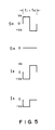
- FIG. 4 is a schematic plan view of a color display panel using an FLC cell 41 according to the present invention.
- S1, S2, S3, ... denote scanning electrodes; I1, I2, I3, ..., signal electrodes; R, a red pixel provided with a red color filter layer; G, a green pixel provided with a green color filter layer; and B, a vlue pixel provided with a green color filter layer.
- Figure 5 shows signal waveforms for driving such a color display panel.
- a scanning selection signal shown at S S are sequentially applied to the scanning electrodes S1, S2, ...
- the scanning selection signal may be sequentially applied to a first scanning electrode S1, ... and an N-th scanning electrode in that order; or may be first sequentially applied to odd-numbered (or even-numbered) scanning electrodes and then sequentially applied to even-numbered (or odd-numbered) scanning electrodes.
- a signal waveform shown at S N is one of a scanning non-selection signal applied to a non-selected scanning electrode.
- Signal waveforms shown at I S and I N are respectively those of information signals applied to signal electrodes I1, I2, ... I N , selectively.
- the signal shown at I S is one for providing a "black” state to a selected pixel on a selected scanning electrode
- I N is one for a "white” state.
- a driving method is described in British Laid-Open Patent Specification GB-A 2141279. More specifically, a voltage of -2V0 exceeding one threshold voltage of an FLC is uniformly applied to pixels on a scanning electrode selected in a phase t1 to provide a "white” state to the pixels based on the first stable state of the FLC.
- a voltage V0 of the information signal I S is applied, a voltage 2V0 exceeding the other threshold voltage of the FLC is applied, the pixel is brought to a "black" state based on a second stable state of the FLC.
- a voltage V0 below the threshold voltage is applied, so that the "white" state formed in phase t1 is retained without change.
- the liquid crystal device according to the present invention can also be applied to driving methods as disclosed in, e.g., GB-A 2156131 and Japanese Laid-Open Application No. 172029/1985.
- a liquid crystal device applied to the systems as described above is formed as a panel with a large area.
- a spacer member e.g., in an elongated shape having a substantially larger length than a diameter such as glass fiber, or a substantially spherical or spheroidal shape such as glass beads, alumina beads or plastic beads, may be disposed between a pair of substrates forming the device so as to retain a uniform cell gap over the entire extension of the device.
- spherical or spheroidal spacers may suitably be used.
- a liquid crystal device comprising a pair of substrates and a ferroelectric liquid crystal disposed between the substrates, at least one of the substrates having thereon a color filter layer and a protection layer for preventing direct contact between the color filter layer and the ferroelectric liquid crystal, and particulate spacers being disposed between the substrates.
- particulate spacers are used in combination with the protection layer covering the color filter layer in the cell, the elution or dissolution of the dye or pigment into the ferroelectric liquid crystal caused by breakage of the protection layer may be prevented, whereby the increase in voltage of a reverse polarity (- ⁇ V0) attributable to the lowering in resistance of the FLC may be prevented.
- FIG. 6 is a sectional view of an embodiment of the liquid crystal device according to this aspect of the present invention applicable to a display of a large area.
- the liquid crystal device includes a color filter layer 61 comprising a blue color filter layer 61(B), a green color filter layer 61(G), and a red color filter layer 61(R), each constituting one color pixel. Covering the color filter layer 61, there is disposed a protection layer 62 for preventing direct contact between the color filter layer 61 and an FLC 65.
- the protection layer 65 can also be provided with an insulating property and an alignment control characteristic.
- Reference numerals 63a and 63b denote substrates comprising, e.g., a glass plate or a plastic film, on which stripe-form transparent electrodes 34a and 34b constituting matrix electrodes of ITO, etc., are provided. Between the pair of substrates 63a and 63b, particulate or bead spacers of a spherical shape such as glass beads, silica beads, alumina beads or plastic beads are disposed so as to control the spacing therebetween.
- alumina beads and silica beads are especially preferred because, they can be obtained to have an average particle size of 1 - 5 ⁇ m with a narrow particle size distribution.
- Particulate spacers 69 used in the present invention may be disposed at a rate of 0.1 - 15 per mm2, preferably 0.5 - 10 per mm2. If more than 15 particles are disposed per mm2, particles 69 can be superposed to increase the tendency of a particle 69 breaking the protection layer 62. On the other hand, less than 0.5 particle per mm2 fails to control a uniform spacing between the substrates 63a and 63b.
- an extremely high accuracy of a cell gap is required so that the tolerance with respect to the uniformity of the cell gap is ⁇ 10 %, whereby 0.5 or more particulate 69 per mm2 is required.
- the particles 69 used in the present invention may be distributed by dispersing, e.g., alumina beads or silica beads in a volatile liquid such as fluorinated methane, fluorinated ethylene, isopropyl alcohol or methanol, and spraying the dispersion onto at least one of the two substrates.
- alumina beads or silica beads in a volatile liquid such as fluorinated methane, fluorinated ethylene, isopropyl alcohol or methanol
- spraying the dispersion onto at least one of the two substrates Alternatively, they can also be distributed by dipping a substrate in such a dispersion of alumina beads or silica beads.
- the color filter layer 61 and the protection layer 62 are similar to the color filter layer 31 and the protection layer 62 explained with reference to Figure 3. Equally, it is preferred that the material constituting the protection layer 62 and the dye or pigment in the color filter layer 61 are not mutually soluble. Further, the transparent electrodes 64b may be disposed on the protection layer instead of between the color filter layer 61 and the protection layer 62. In such a case, a uniaxially orientation-treated alignment control film may preferably be disposed to cover the transparent electrodes.
- the protection layer 62 is formed to have a pencil hardness of HB or harder. In such a case, even if the particulate spacers 69 are disposed at a rate of more than 15 particles per mm2, the breakage of the protection layer 62 can be avoided.
- pencil hardness refers to a hardness measured by means of a “pencil scratch tester for coating films” according to JIS K 5401.
- Examples of transparent insulating resins which may be used for providing a protection layer 62 having a pencil hardness of HB or harder may include rubber-type photoresists, thermosetting acrylic resin, polyimide, polyparaxylylene (e.g., Palylene (trade name), Union Carbide Corp.), polyethylene, polystyrene and polycarbonate.
- the protection layer may for example be formed by spinner coating.
- the protection layer 62 having such a hardness may also be formed with a transparent insulating inorganic compound such as SiO2, Al2O3, TiO2, ZrO2, MgF2 or SiO.
- the protection layer 62 When the protection layer 62 is formed to have a pencil hardness of HB or harder, the breakage of the protection layer due to particulate spacers can be avoided. As a result, a surface roughness or unevenness on the substrate surface causing alignment defects is avoided, so that in a liquid crystal layer sandwiched between the substrates having a good planarity, a liquid crystal phase region is gradually developed during a cooling stage from the isotropic phase to the liquid crystal phase thereby to form a liquid crystal phase of a uniform monodomain.
- DOBAMBC showing a ferroelectric liquid crystal phase is taken as an example of a liquid crystal
- the DOBAMBC is gradually cooled from its isotropic phase
- it is transformed into smectic A (SmA) phase at about 115°C.
- SmA smectic A
- a substrate is provided with a uniaxial orientation treatment such as rubbing or oblique vapor deposition of SiO2
- a monodomain wherein liquid crystal molecules are aligned with their molecular axes extending in parallel with the substrate and in one direction.
- DOBAMBC is transformed into chiral smectic C phase (SmC* phase) at a specific temperature between about 90 - 75°C depending on the liquid crystal layer thickness.
- the liquid crystal layer thickness is about 2 ⁇ or less, the helical structure of SmC* phase is unwound or released to provide a ferroelectric liquid crystal having at least a first stable state and a second stable state.
- the protection layer 62 used in the present invention when the protection layer 62 used in the present invention is caused to have a pencil hardness of HB or harder, the breakage of the protection layer 62 due to pressing by particulate spacers may be avoided, whereby the dissolution of the dye or pigment in the color filter into the FLC 65 is prevented, so that the problem arising from the decrease in resistance of the FLC is prevented from occurring.
- the color filter layer 61 is formed to have substantially the same thickness, so that even if a protection layer 62, transparent electrodes 64b, and an alignment control film 71 are successively formed thereon, the surface contacting the FLC 65 is kept substantially flat.
- steps or stepwise elevations possibly formed on the surface contacting the FLC 65 of the substrate 63b having the color filter may be suppressed to 1000 ⁇ or less, preferably 500 ⁇ or less. If the steps are formed to exceed 1000 ⁇ , particularly 1200 ⁇ , a liquid crystal device with no flattening layer results in zigzag or edge-like line defects.
- the thickness of the alignment control film 71 may be set to generally 10 ⁇ - 1 ⁇ m, preferably 100 ⁇ - 3000 ⁇ , while it depends on the thickness of the FLC layer.
- Figures 8A - 8F illustrate steps for forming color pixels of three colors R, G and B with reference to a specific embodiment.
- a positive-type resist (“OFPR 77” (trade name), mfd. by Tokyo Ohka K.K.) was applied by a spinner coater to form a 1.0 ⁇ -thick resist layer 82 ( Figure 8A).
- the resist layer 82 was exposed to light through a mask 83 with a prescribed pattern ( Figure 8B), followed by development with a developer liquid prescribed for OFPR 77 series to form a pattern of prescribed stripes for lifting-off (Figure 8C).
- the glass substrate 81 provided with a pattern 82a for lifting-off was placed at a prescribed position in a vacuum evaporator, in which was further disposed a molybdenum boat for an evaporation source containing nickel phthalocyanine as an evaporating blue colorant. Then, the nickel phthalocyanine was evaporated at 470°C to be deposited in a thickness of 5500 ⁇ on the face of the substrate 81 having the lifting-off pattern to form a colorant layer 84 ( Figure 8D).
- the substrate 81 having the lifting-off pattern 82a and the colorant layer was dipped in the developer liquid for OFPR 77 series under stirring for 5 minutes to remove the resist pattern 82a together with the portion of the colorant layer 84a deposited on the pattern from the substrate, thereby to form a blue stripe filter 84b.
- green and red stripe filters were respectively prepared by repeating the steps as described with reference to Figures 8A - 8E.
- Lead phthalocyanine was used as a green colorant for vapor deposition to form a 5500 ⁇ -thick green stripe filter 84g.
- Reference numerals 91a and 91b denote substrates (glass plates) on which a transparent electrode of, e.g., In2O3, SnO2, ITO (indium-tin-oxide), etc., is disposed, respectively.
- a liquid crystal of, e.g., an SmC*-phase in which liquid crystal molecular layers 92 are oriented perpendicular to surfaces of the glass plates is hermetically disposed therebetween.
- Full lines 93 show liquid crystal molecules.
- Each liquid crystal molecule 93 has a dipole moment (P ⁇ ) 94 in a direction perpendicular to the axis thereof.
- liquid crystal molecules 93 When a voltage higher than a certain threshold level is applied between electrodes formed on the substrates 91a and 91b, a helical structure of the liquid crystal molecules 93 is unwound or released to change the alignment direction of respective liquid crystal molecules 93 so that the dipole moments (P ⁇ ) 94 are all directed in the direction of the electric field.
- the liquid crystal molecules 93 have an elongated shape and show refractive anisotropy between the long axis and the short axis thereof.
- the liquid crystal cell when, for instance, polarizers arranged in a cross nicol relationship, i.e., with their polarizing directions crossing each other, are disposed on the upper and the lower surfaces of the glass plates, the liquid crystal cell thus arranged functions as a liquid crystal optical modulation device, of which optical characteristics vary depending upon the polarity of an applied voltage.
- the helical structure of the liquid crystal molecules is unwound to provide a non-helical structure even in the absence of an electric field whereby the dipole moment assumes either of the two states, i.e., Pa in an upper direction 104a or Pb in a lower direction 104b as shown in Figure 10.
- electric field Ea or Eb higher than a certain threshold level and different from each other in polarity as shown in Figure 10 is applied to a cell having the above-mentioned characteristics, the dipole moment is directed either in the upper direction 104a or in the lower direction 104b depending on the vector of the electric field Ea or Eb.
- the liquid crystal molecules are oriented in either of a first stable state 103a and a second stable state 103b.
- the response speed is quite fast.
- Second is that the orientation of the liquid crystal shows bistability.
- the second advantage will be further explained, e.g., with reference to Figure 10.
- the electric field Ea is applied to the liquid crystal molecules, they are oriented in the first stable state 103a. This state is stably retained even if the electric field is removed.
- the electric field Eb of which direction is opposite to that of the electric field Ea is applied thereto, the liquid crystal molecules are oriented to the second stable state 103b, whereby the directions of molecules are changed. This state is also stably retained even if the electric field is removed.
- the liquid crystal molecules are placed in the respective orientation states.
- the thickness of the cell is as thin as possible and generally 0.5 to 20 ⁇ , particularly 1 to 5 ⁇ .
- a liquid crystal-electrooptical device having a matrix electrode structure in which the ferroelectric liquid crystal of this kind is used is proposed, e.g., in the specification of U.S. Patent No. 4367924 by Clark and Lagerwall.
- chiral smectic liquid crystals are most preferred, among which liquid crystals showing chiral smectic C phase (SmC*), H phase (SmH*), I phase (SmI*), F phase (SmF*) or G phase (SmG*) are suitable.
- examples of the FLC usable in the present invention include p-decyloxybenzylidene-p′-amino-2-methylbutylcinnamate (DOBAMBC), p-hexyloxybenzylidene-p′-amino-2-chloropropylcinnamate (HOBACPC), p-decyloxybenzylidene-p′-amino-2-methylbutyl- ⁇ -cyanocinnamate (DOBAMBCC), p-tetradecyloxybenzylidene-p′-amino-2-methylbutyl- ⁇ -cyanocinnamate (TDOBAMBCC), p-octyloxybenzylidene-p′-amino-2-methylbutyl- ⁇ -chlorocinnamate (OOBAMBCC), p-octyloxybenzylidene-p′-amino-2-methylbutyl- ⁇ -methylcin
- FLC compounds may be used singly or in combination of two or more species, or may be mixed with another non-ferroelectric liquid crystal, such as nematic liquid crystal, cholesteric liquid crystal (chiral nematic liquid crystal) or smectic liquid crystal.
- the above mentioned FLC may be one having a helical structure as shown in Figure 9 or one having a non-helical structure as shown in Figure 10.
- a driving method wherein an FLC having a negative dielectric anisotropy is used and an AC bias is applied between two electrodes to provide a non-helical structure with bistability.
- a driving method wherein such an AC bias is applied to an FLC device having a liquid crystal layer thin enough to provide a non-helical structure by itself.
- a square glass plate provided with ITO stripe electrodes each having a width of 62.5 ⁇ m and at a pitch of 100 ⁇ m was provided and disposed with its side having the ITO electrodes directed downward in a vacuum evaporator, in which a copper phthalocyanine pigment (blue) was vapor-deposited in a thickness of 2000 ⁇ . Then, the vapor-deposited layer of copper phthalocyanine was patterned by a prescribed photolithographic process.
- a 5 wt.% solution of a polyamic acid, a polyimide precursor (dehydro-condensation product of pyromellitic dianhydride and 4,4′-diaminodiphenyl ether) in N-methylpyrrolidone was spinner-coated and heat-cured to form an 800 ⁇ -thick film.
- the surface of the polyimide film after the heat curing was rubbing-treated with velvet in parallel with the longitudinal direction of the stripe electrodes.
- the thus prepared electrode plate is referred to as the electrode plate A.
- an electrode plate B was prepared in quite the same manner as above except that the preparation of the copper phthalocyanine color filter layer was omitted and the rubbing direction was transverse to the longitudinal direction of the stripe electrodes.
- thermosetting epoxy adhesive was applied by screen printing, and the electrode plate A and the electrode plate B were superposed with each other so that their stripe electrode pattern crossed at right angles while retaining the spacing therebetween at 2 ⁇ m with polyimide spacers.
- liquid crystal composition A (showing SmC* phase at 20°C - 78°C) in isotropic phase was injected through the injection port, which was then sealed.
- the cell was then gradually cooled at a rate of 0.5°C/hr and maintained at 40°C, where the cell after being provided with a pair of polarizers arranged in cross nicols was observed through a microscope.
- a monodomain of SmC* phase assuming a non-helical structure with no alignment defects was observed to be formed.
- a liquid crytal cell for comparison was prepared in quite the same manner as in the above Example 1 except that a monolayer of a silane coupling agent was used instead of the polyimide protection layer, whereby a monodomain of SmC* phase was observed to be formed similarly as in Example 1.
- Example 1 The two types of liquid crystal cells prepared in Example 1 and Comparative Example 1 were allowed to stand for 96 hours under the conditions of a temperature of 80°C and a relative humidity of 60 %. Thereafter, the resistivities of the respective liquid crystal layers were measured. The results are shown in the following Table 1.
- resistivity values ( ⁇ cm) measured with respect to the above examples and also with respect to the other examples appearing hereinafter were obtained by applying rectangular pulses according to the dual frequency method by using a circuit as shown in Figure 11, and calculating R LC ( ⁇ cm) from the following formula.
- I1 4f1 ⁇ C LC ⁇ V + V/R LC
- I2 4f2 ⁇ C LC ⁇ V + V/R LC
- the respective liquid crystal display cells after standing for 96 hours were, after disposition of cross nicol polarizers, driven by applying a signal of 20 volts between the electrodes, whereby the liquid crystal cell according to Example 1 provided a display quality including a good contrast similar to that obtained before the standing, whereas the one according to Comparative Example 1 caused undesirable inversion phenomenon compared with that obtained before the standing.
- Liquid crystal cells were prepared in quite the same manner as in Example 1 except that lead phthalocyanine (Example 2) and Perylene Red (Example 3) were respectively used instead of copper phthalocyanine used in Example 1.
- the liquid crystal cells were subjected to the standing or durability test as described above, whereby the results similar to those in Example 1 were obtained.
- a liquid crystal cell was prepared in the same manner as in Example 1 except that a colored polyimide film prepared as described below was used as a color filter layer instead of the copper phthalocyanine vapor-deposited layer, whereby similar results as those obtained in Example 1 were obtained.
- the resultant paste was taken in a four-necked flask provided with a reflux cooler, 100 parts of water and 21 parts of N-diethylaminoethylamine were added thereto, and the mixture was stirred for 12 hours at room temperature and heated at 60°C for 1 hour. After the completion of the reaction, the product was subjected to filtration, washing with water and drying to obtain blue powder of a copper phthalocyanine derivative. The blue powder was subjected to elementary analysis, whereby the compound was found to be a copper phthalocyanine derivative to which about three of the following group had been introduced:
- the dispersion liquid was applied by a spinner coater to provide a 500 ⁇ -thick colored polyimide film after heat-curing.
- An FLC device was prepared in the same manner as in Example 1 except that the electrode plate was further provided with a 1 ⁇ m-thick layer of a negative resist resin ("ODUR", mfd. by Tokyo Ohka K.K.) as a second protection layer between the color filter layer and the polyimide layer, and the device was subjected to the durability test.
- ODUR negative resist resin
- Electrode plates A and B were prepared in the same manner as in Example 1.
- alumina beads having an average particle size of about 5 ⁇ m were dispersed in 400 cc of methanol, and the above electrode plate B was dipped in the resultant dispersion, pulled up and dried to provide the electrode plate B with aluminia beads dispersed thereon.
- thermosetting epoxy adhesive was applied by screen printing, and the electrode plate A and the electrode plate B prepared above were superposed with each other. Then, while applying an external pressure of 5 kg/cm2 uniformly from outside the electrode plate A, the adhesive was cured under the pressure.
- the above mentioned liquid crystal composition A was injected through the injection port, which was then sealed up.
- the cell was gradually cooled and maintained at 40°C, where the cell after being provided with a pair of polarizers arranged in cross nicols was observed through a microscope.
- a monodomain of SmC* phase assuming a non-helical structure with no alignment defects was observed to be formed.
- a liquid crystal cell for comparison was prepared in quite the same manner as in the above Example 6 except that glass fiber of about 5 ⁇ m diameter was used instead of the alumina beads, whereby a monodomain of SmC* phase was observed to be formed similarly as in Example 6.
- Example 6 The two types of liquid crystal cells prepared in Example 6 and Comparative Example 2 were allowed to stand for 96 hours under the conditions of a temperature of 80°C and a relative humidity of 60 %. Thereafter, the resistivities of the respective liquid crystal layers were measured. Then results are shown in the following Table 3.
- a liquid crystal cell for comparison was prepared in quite the same manner as in the above Example 6 except that alumina beads having an average particle size of about 1 ⁇ m were used instead of the alumina beads having an average particle size of about 5 ⁇ m, whereby a monodomain of SmC* phase was observed to be formed similarly as in Example 6.
- the liquid crystal cell was allowed to stand for 96 hours under the conditions of a temperature of 80°C and a relative humidity of 60 %. Thereafter, the resistivity of the respective liquid crystal layers was measured in the same manner, whereby the resistivity after the standing for 96 hours was 2.5 ⁇ 1010 ⁇ cm similarly as that of the initial stage.
- Liquid crystal cells were prepared in quite the same manner as in Example 7 except that lead phthalocyanine (Example 8) and Perylene Red (Example 9) were respectively used instead of copper phthalocyanine used in Example 7.
- the liquid crystal cells were subjected to the standing or durability test as described above, whereby the results similar to those in Example 7 were obtained.
- a liquid crystal cell was prepared in the same manner as in Example 7 except that a colored polyimide film as used in Example 1 was used as a color filter layer instead of the copper phthalocyanine vapor-deposited layer, whereby similar results as those obtained in Example 7 were obtained.
- the present invention provides a stable color display for a long period of use of a liquid crystal device for color display, particularly for a color television display panel.
- a protection layer as described above is omitted from a conventional dot matrix-type liquid crystal device using a TN-liquid crystal and provided with a color filter layer
- the TN-liquid crystal layer also causes a decrease in resistance.
- a display state different from that obtained corresponding to written information does not result at the time of falling-down of a writing pulse, whereby no consideration on the decrease in resistance is required.
- a polyetheramide-imide resin (“HL-1100” (trade name), mfd. by Hitachi Kasei K.K.) was applied by means of a spinner coater on a glass plate and heat-cured to form a 1 ⁇ m-thick film.
- the surface hardness of the film was measured to be a pencil hardness of 5H according to JIS K 5401.
- copper phthalocyanine pigment was vapor-deposited in a thickness of 2000 ⁇ on a square glass plate by means of a vacuum evaporator.
- the above mentioned polyetheramide-imide resin was formed in a thickness of 1 ⁇ m in the manner as described above.
- a 500 ⁇ -thick ITO film was formed by sputtering and patterned into stripe electrodes. Further thereon, a polyimide-forming solution ("PIQ" (trade name), mfd. by Hitachi Kasei K.K.) was applied by means of a spinner coater rotating at 3000 rpm and heated at 150°C for 30 minutes to form a 2000 ⁇ -thick polyimide film. Thereafter, the surface of the polyimide film was rubbing-treated in parallel with the longitudinal direction of the stripe electrodes to provide a first electrode plate.
- PIQ polyimide-forming solution
- a second electrode plate was prepared in the same manner as described above for preparation of the first electrode plate except that the copper phthalocyanine vapor-deposited layer was omitted and the rubbing direction was perpendicular to the longitudinal direction of the stripe electrodes.
- alumina beads having an average particle size of about 5 ⁇ m were dispersed in 400 cc of methanol, and the above mentioned second electrode plate was dipped in the resultant dispersion, pulled up and dried to disperse the alumina beads on the second electrode plate.
- thermosetting epoxy adhesive was applied by screen printing, and the first and second electrode plates were superposed with each other. Then, while applying a pressure of 5 kg/cm2 uniformly from outside the first electrode plate, the adhesive was cured under the pressure.
- the above mentioned liquid crystal composition A was injected through the injection port, which was then sealed up.
- the cell was gradually cooled and maintained at 40°C, where the cell after being provided with a pair of polarizers arranged in cross nicols was observed through a microscope.
- a monodomain of SmC* phase assuming a non-helical structure with no alignment defects was observed to be formed.
- a liquid crystal device was prepared in the same manner as in Example 11 except that polyacrylonitrile resin was used instead of the polyetheramide-imide.
- the surface hardness of the polyacrylonitrile film was measured to be a pencil hardness of HB according to the method used in Example 11.
- the liquid crystal device prepared above was observed through a cross nicol-polarizing microscope, whereby a device having no alignment defects was found to be formed without breakage of the protection film due to the bead spacers.
- a liquid crystal device was prepared in the same manner as in Example 11 except that polyvinyl alcohol resin was used instead of the polyetheramide-imide resin.
- the surface hardness of the polyvinyl alcohol film used herein was measured to be a pencil hardness of 2B according to the method in Example 11.
- the liquid crystal device prepared above was observed through a cross nicol-polarizing microscope, whereby defects were observed and noticeable alignment defects in the liquid crystal layer were also observed at the defects.
- the three liquid crystal cells were subjected to driving, whereby the liquid crystal cells prepared in Example 11 and 12 showed a stable driving characteristic, but the driving of the liquid crystal cell prepared in Comparative Example 3 was unstable.
Applications Claiming Priority (6)
| Application Number | Priority Date | Filing Date | Title |
|---|---|---|---|
| JP60285283A JPH0680450B2 (ja) | 1985-12-18 | 1985-12-18 | カイラルスメクチック液晶素子 |
| JP285283/85 | 1985-12-18 | ||
| JP61012338A JPH07117665B2 (ja) | 1986-01-22 | 1986-01-22 | カイラルスメクチック液晶素子 |
| JP12338/86 | 1986-01-22 | ||
| JP41556/86 | 1986-02-28 | ||
| JP61041556A JP2627063B2 (ja) | 1986-02-28 | 1986-02-28 | 液晶装置 |
Publications (3)
| Publication Number | Publication Date |
|---|---|
| EP0226218A2 true EP0226218A2 (de) | 1987-06-24 |
| EP0226218A3 EP0226218A3 (en) | 1989-01-25 |
| EP0226218B1 EP0226218B1 (de) | 1993-07-14 |
Family
ID=27279801
Family Applications (1)
| Application Number | Title | Priority Date | Filing Date |
|---|---|---|---|
| EP86117613A Expired - Lifetime EP0226218B1 (de) | 1985-12-18 | 1986-12-17 | Flüssigkristallvorrichtung |
Country Status (4)
| Country | Link |
|---|---|
| US (1) | US5078475A (de) |
| EP (1) | EP0226218B1 (de) |
| DE (1) | DE3688700T2 (de) |
| ES (1) | ES2043600T3 (de) |
Cited By (15)
| Publication number | Priority date | Publication date | Assignee | Title |
|---|---|---|---|---|
| EP0288304A2 (de) * | 1987-04-22 | 1988-10-26 | Sharp Kabushiki Kaisha | Flüssigkristall-Anzeigevorrichtung |
| US4786148A (en) * | 1986-12-10 | 1988-11-22 | Canon Kabushiki Kaisha | Color filter having different primary color pigment densities, inter alia |
| EP0296429A2 (de) * | 1987-06-25 | 1988-12-28 | International Business Machines Corporation | Flüssigkristall-Anzeigevorrichtung mit einer Farbfilterschicht |
| EP0299508A1 (de) * | 1987-07-17 | 1989-01-18 | Nippon Paint Co., Ltd. | Herstellung einer Farbanzeige |
| EP0311979A2 (de) * | 1987-10-15 | 1989-04-19 | Displaytech, Incorporated | Elektrooptische Schaltvorrichtungen mit ferroelektrischen Flüssigkristallen |
| EP0326112A2 (de) * | 1988-01-29 | 1989-08-02 | Toppan Printing Co., Ltd. | Elektrodenstruktur für Anzeigevorrichtungen und ihr Herstellungsverfahren |
| EP0356044A2 (de) * | 1988-08-19 | 1990-02-28 | Seiko Instruments Inc. | Flüssigkristall-Anzeigevorrichtung und ihr Herstellungsverfahren |
| US5042920A (en) * | 1988-11-10 | 1991-08-27 | Kabushiki Kaisha Toshiba | Liquid crystal display device and color filter for use with the liquid crystal display device with two resin layers over the color filter |
| EP0544285A1 (de) * | 1991-11-26 | 1993-06-02 | Eastman Kodak Company | Photosensitive, quervernetzbare Polyester-Ausgleichsschichten für Flüssigkristall-Displays |
| US5312703A (en) * | 1989-09-14 | 1994-05-17 | Basf Aktiengesellschaft | Reversible or irreversible production of an image |
| US5538824A (en) * | 1991-02-28 | 1996-07-23 | Basf Aktiengesellschaft | Reversible or irreversible production of an image |
| EP0740184A2 (de) * | 1995-04-28 | 1996-10-30 | Canon Kabushiki Kaisha | Flüssigkristallvorrichtung, Verfahren zu ihrer Herstellung, und Flüssigkristallgerät |
| WO1996035139A1 (en) * | 1995-05-05 | 1996-11-07 | Specialty Coating Systems, Inc. | Flat panel display with parylene barrier and protective films |
| US5610740A (en) * | 1991-04-16 | 1997-03-11 | Seiko Instruments Inc. | Color electrooptical device |
| US6203950B1 (en) | 1991-02-25 | 2001-03-20 | Shinto Chemitron Co. Ltd. | Method for manufacturing a color filter |
Families Citing this family (39)
| Publication number | Priority date | Publication date | Assignee | Title |
|---|---|---|---|---|
| US5572345A (en) * | 1986-03-11 | 1996-11-05 | Semiconductor Energy Laboratory Co., Ltd. | Liquid crystal device for preventing short circuiting therein |
| JPH0690375B2 (ja) * | 1986-04-17 | 1994-11-14 | キヤノン株式会社 | 液晶装置 |
| JPH03248125A (ja) * | 1990-02-26 | 1991-11-06 | Sharp Corp | 液晶表示素子 |
| JP2991258B2 (ja) * | 1990-11-16 | 1999-12-20 | キヤノン株式会社 | 強誘電性液晶素子および液晶表示装置 |
| JP2835787B2 (ja) * | 1991-03-22 | 1998-12-14 | キヤノン株式会社 | 強誘電性液晶素子 |
| JP2737032B2 (ja) * | 1991-03-28 | 1998-04-08 | キヤノン株式会社 | 液晶セル |
| JP2847331B2 (ja) * | 1991-04-23 | 1999-01-20 | キヤノン株式会社 | 液晶表示装置 |
| JP2952075B2 (ja) * | 1991-06-12 | 1999-09-20 | キヤノン株式会社 | 液晶素子の製造法 |
| JP2974520B2 (ja) * | 1991-10-25 | 1999-11-10 | キヤノン株式会社 | 電極基板及び液晶素子 |
| JP3082114B2 (ja) * | 1992-07-02 | 2000-08-28 | 富士通株式会社 | 液晶表示装置 |
| JP2814171B2 (ja) * | 1992-08-19 | 1998-10-22 | キヤノン株式会社 | 液晶パネルの製造方法 |
| US5552911A (en) * | 1992-10-19 | 1996-09-03 | Canon Kabushiki Kaisha | Color liquid crystal display device having varying cell thickness and varying pixel areas |
| JP3080492B2 (ja) * | 1992-11-30 | 2000-08-28 | シャープ株式会社 | カラー液晶表示装置 |
| US5587211A (en) * | 1994-04-18 | 1996-12-24 | Canon Kabushiki Kaisha | Liquid crystal device and liquid crystal apparatus including same |
| US5905558A (en) * | 1995-08-29 | 1999-05-18 | Canon Kabushiki Kaisha | Circuit plate, process for producing same and liquid crystal device including same |
| JP3299869B2 (ja) * | 1995-09-27 | 2002-07-08 | シャープ株式会社 | 液晶表示装置とその製造方法 |
| JP3305212B2 (ja) * | 1995-11-09 | 2002-07-22 | キヤノン株式会社 | 液晶素子用の基板、液晶素子、およびそれらの製造方法 |
| US5858482A (en) * | 1996-07-26 | 1999-01-12 | Canon Kabushiki Kaisha | Liquid crystal device and process for production thereof |
| TW439007B (en) * | 1996-09-11 | 2001-06-07 | Canon Kk | Process and apparatus for producing electrode plate and process for producing liquid crystal device including the plate |
| US6028978A (en) * | 1996-12-16 | 2000-02-22 | Ngk Insulators, Ltd. | Display device having a colored layer disposed between a displacement transmitting section and an optical waveguide plate |
| US5989451A (en) * | 1997-02-07 | 1999-11-23 | Queen's University At Kingston | Compounds and methods for doping liquid crystal hosts |
| JP3883641B2 (ja) * | 1997-03-27 | 2007-02-21 | 株式会社半導体エネルギー研究所 | コンタクト構造およびアクティブマトリクス型表示装置 |
| JPH10332925A (ja) * | 1997-06-02 | 1998-12-18 | Canon Inc | カラーフィルタ基板とその製造方法、該基板を用いた液晶素子 |
| JP3176565B2 (ja) * | 1997-07-14 | 2001-06-18 | 三菱電機株式会社 | 液晶表示装置 |
| US6054395A (en) * | 1997-10-24 | 2000-04-25 | Micron Technology, Inc. | Method of patterning a semiconductor device |
| WO1999024859A1 (fr) * | 1997-11-06 | 1999-05-20 | Ngk Insulators, Ltd. | Affichage et procede de fabrication de ce dernier |
| US6335779B1 (en) * | 1999-01-27 | 2002-01-01 | Mistubishi Denki Kaubshiki Kaisha | Liquid crystal display apparatus and method for producing TFT using therefor |
| US7547579B1 (en) * | 2000-04-06 | 2009-06-16 | Micron Technology, Inc. | Underfill process |
| US6674494B2 (en) * | 2000-12-28 | 2004-01-06 | Optrex Corporation | Liquid crystal optical element and test method for its boundary layer |
| CN1842745B (zh) * | 2003-08-28 | 2013-03-27 | 株式会社半导体能源研究所 | 薄膜晶体管、薄膜晶体管的制造方法、以及显示器件的制造方法 |
| US20050100690A1 (en) * | 2003-11-06 | 2005-05-12 | Optical Coating Laboratory Inc., A Jds Uniphase Company | Dyed polymer coating for display panel |
| WO2009050294A2 (en) * | 2007-10-19 | 2009-04-23 | Seereal Technologies S.A. | Light modulating device |
| JP2009276743A (ja) * | 2008-04-14 | 2009-11-26 | Seiko Epson Corp | 液晶表示装置、電子機器 |
| TWI473257B (zh) * | 2010-02-26 | 2015-02-11 | United Microelectronics Corp | 影像感測元件的製造方法及其重工方法 |
| US8084289B2 (en) * | 2010-02-26 | 2011-12-27 | United Microelectronics Corp. | Method of fabricating image sensor and reworking method thereof |
| US9632362B2 (en) * | 2014-07-03 | 2017-04-25 | Innolux Corporation | Liquid crystal display panel and liquid crystal display device containing the same |
| US9518872B2 (en) * | 2014-10-14 | 2016-12-13 | Kidde Technologies, Inc. | Thermal sensor |
| TWM524483U (zh) * | 2016-01-19 | 2016-06-21 | Nanobit Tech Co Ltd | 3d高分子分散液晶複合層結構 |
| CN113867063B (zh) * | 2021-10-28 | 2022-12-16 | 华南理工大学 | 一种铁电螺旋液晶材料及其实现二次谐波增强的方法 |
Citations (5)
| Publication number | Priority date | Publication date | Assignee | Title |
|---|---|---|---|---|
| US4367924A (en) | 1980-01-08 | 1983-01-11 | Clark Noel A | Chiral smectic C or H liquid crystal electro-optical device |
| GB2141279A (en) | 1983-04-19 | 1984-12-12 | Canon Kk | Electro-optical display devices |
| JPS60172029A (ja) | 1984-02-17 | 1985-09-05 | Canon Inc | 液晶装置 |
| GB2156131A (en) | 1984-01-23 | 1985-10-02 | Canon Kk | Display devices |
| US4767924A (en) | 1986-08-19 | 1988-08-30 | B.A.T. Cigarettenfabriken Gmbh | Apparatus for optical monitoring with a high pressure lamp connected to a fiber optic cable |
Family Cites Families (22)
| Publication number | Priority date | Publication date | Assignee | Title |
|---|---|---|---|---|
| US3912365A (en) * | 1971-07-26 | 1975-10-14 | Research Frontiers Inc | Method and apparatus for maintaining the separation of plates |
| JPS54151055A (en) * | 1978-05-18 | 1979-11-27 | Seiko Epson Corp | Liquid crystal optical device |
| JPS57613A (en) * | 1980-06-02 | 1982-01-05 | Asahi Glass Co Ltd | Liquid crystal display element |
| JPS5929225A (ja) * | 1982-08-11 | 1984-02-16 | Matsushita Electric Ind Co Ltd | 液晶表示パネルのカラ−フイルタ−製造方法 |
| JPS5961818A (ja) * | 1982-10-01 | 1984-04-09 | Seiko Epson Corp | 液晶表示装置 |
| FR2542893B1 (fr) * | 1983-03-18 | 1985-06-21 | Thomson Csf | Ecran de visualisation en couleurs a cristal liquide smectique |
| JPS59180525A (ja) * | 1983-03-31 | 1984-10-13 | Citizen Watch Co Ltd | カラ−液晶表示パネル |
| US4709991A (en) * | 1983-04-26 | 1987-12-01 | Seiko Epson Kabushiki Kaisha | Liquid crystal display with barrier layer to reduce permeability |
| JPS6017720A (ja) * | 1983-07-12 | 1985-01-29 | Canon Inc | 液晶装置 |
| JPS6084529A (ja) * | 1983-10-17 | 1985-05-13 | Nippon Denso Co Ltd | 液晶素子 |
| IL70116A (en) * | 1983-11-02 | 1987-02-27 | Stolov Michael | Liquid crystal device for displaying multicolor images |
| US4632514A (en) * | 1984-01-31 | 1986-12-30 | Matsushita Electric Industrial Co., Ltd. | Color liquid crystal display apparatus |
| JPS60184227A (ja) * | 1984-03-02 | 1985-09-19 | Hitachi Ltd | 液晶表示装置およびその製造方法 |
| JPH0617508B2 (ja) * | 1984-04-13 | 1994-03-09 | 新日本製鐵株式会社 | 電磁鋼板の耳割れ破断防止方法 |
| JPS60220316A (ja) * | 1984-04-16 | 1985-11-05 | Canon Inc | 液晶光学素子 |
| US4744637A (en) * | 1984-10-05 | 1988-05-17 | Canon Kabushiki Kaisha | Liquid crystal device with a protective layer of a particular coefficient of expansion |
| JPS61113030A (ja) * | 1984-11-07 | 1986-05-30 | Dainippon Printing Co Ltd | 多色液晶表示装置 |
| US4712878A (en) * | 1985-01-18 | 1987-12-15 | Canon Kabushiki Kaisha | Color image forming apparatus comprising ferroelectric smectic liquid crystal having at least two stable states |
| JPH0718995B2 (ja) * | 1985-02-19 | 1995-03-06 | キヤノン株式会社 | 液晶素子 |
| JPS61260222A (ja) * | 1985-05-15 | 1986-11-18 | Canon Inc | 液晶素子 |
| US4775225A (en) * | 1985-05-16 | 1988-10-04 | Canon Kabushiki Kaisha | Liquid crystal device having pillar spacers with small base periphery width in direction perpendicular to orientation treatment |
| JPH072720B2 (ja) * | 1986-09-11 | 1995-01-18 | チッソ株式会社 | シクロヘキシルフエニルピリダジン類 |
-
1986
- 1986-12-17 ES ES86117613T patent/ES2043600T3/es not_active Expired - Lifetime
- 1986-12-17 DE DE86117613T patent/DE3688700T2/de not_active Expired - Fee Related
- 1986-12-17 EP EP86117613A patent/EP0226218B1/de not_active Expired - Lifetime
-
1989
- 1989-03-27 US US07/328,706 patent/US5078475A/en not_active Expired - Fee Related
Patent Citations (5)
| Publication number | Priority date | Publication date | Assignee | Title |
|---|---|---|---|---|
| US4367924A (en) | 1980-01-08 | 1983-01-11 | Clark Noel A | Chiral smectic C or H liquid crystal electro-optical device |
| GB2141279A (en) | 1983-04-19 | 1984-12-12 | Canon Kk | Electro-optical display devices |
| GB2156131A (en) | 1984-01-23 | 1985-10-02 | Canon Kk | Display devices |
| JPS60172029A (ja) | 1984-02-17 | 1985-09-05 | Canon Inc | 液晶装置 |
| US4767924A (en) | 1986-08-19 | 1988-08-30 | B.A.T. Cigarettenfabriken Gmbh | Apparatus for optical monitoring with a high pressure lamp connected to a fiber optic cable |
Cited By (26)
| Publication number | Priority date | Publication date | Assignee | Title |
|---|---|---|---|---|
| US4786148A (en) * | 1986-12-10 | 1988-11-22 | Canon Kabushiki Kaisha | Color filter having different primary color pigment densities, inter alia |
| EP0288304B1 (de) * | 1987-04-22 | 1993-03-17 | Sharp Kabushiki Kaisha | Flüssigkristall-Anzeigevorrichtung |
| EP0288304A2 (de) * | 1987-04-22 | 1988-10-26 | Sharp Kabushiki Kaisha | Flüssigkristall-Anzeigevorrichtung |
| EP0296429A2 (de) * | 1987-06-25 | 1988-12-28 | International Business Machines Corporation | Flüssigkristall-Anzeigevorrichtung mit einer Farbfilterschicht |
| EP0296429A3 (de) * | 1987-06-25 | 1991-02-27 | International Business Machines Corporation | Flüssigkristall-Anzeigevorrichtung mit einer Farbfilterschicht |
| US4902592A (en) * | 1987-07-17 | 1990-02-20 | Nippon Paint Co., Ltd. | Production of color display |
| EP0299508A1 (de) * | 1987-07-17 | 1989-01-18 | Nippon Paint Co., Ltd. | Herstellung einer Farbanzeige |
| EP0311979A3 (de) * | 1987-10-15 | 1989-12-27 | Displaytech, Incorporated | Elektrooptische Schaltvorrichtungen mit ferroelektrischen Flüssigkristallen |
| EP0311979A2 (de) * | 1987-10-15 | 1989-04-19 | Displaytech, Incorporated | Elektrooptische Schaltvorrichtungen mit ferroelektrischen Flüssigkristallen |
| EP0326112A3 (en) * | 1988-01-29 | 1990-08-22 | Toppan Printing Co., Ltd. | Electrode plate for display device and method for preparation thereof |
| EP0326112A2 (de) * | 1988-01-29 | 1989-08-02 | Toppan Printing Co., Ltd. | Elektrodenstruktur für Anzeigevorrichtungen und ihr Herstellungsverfahren |
| US5045418A (en) * | 1988-01-29 | 1991-09-03 | Toppan Printing Co., Ltd. | Electrode plate for display device and method for preparation thereof |
| EP0356044A2 (de) * | 1988-08-19 | 1990-02-28 | Seiko Instruments Inc. | Flüssigkristall-Anzeigevorrichtung und ihr Herstellungsverfahren |
| EP0356044A3 (en) * | 1988-08-19 | 1990-06-20 | Seiko Instruments Inc. | Liquid crystal display device and method of producing the same |
| US5580436A (en) * | 1988-08-19 | 1996-12-03 | Seiko Instruments Inc. | Method of producing a multicolor liquid crystal display device |
| US5042920A (en) * | 1988-11-10 | 1991-08-27 | Kabushiki Kaisha Toshiba | Liquid crystal display device and color filter for use with the liquid crystal display device with two resin layers over the color filter |
| US5312703A (en) * | 1989-09-14 | 1994-05-17 | Basf Aktiengesellschaft | Reversible or irreversible production of an image |
| US6203950B1 (en) | 1991-02-25 | 2001-03-20 | Shinto Chemitron Co. Ltd. | Method for manufacturing a color filter |
| US5538824A (en) * | 1991-02-28 | 1996-07-23 | Basf Aktiengesellschaft | Reversible or irreversible production of an image |
| US5610740A (en) * | 1991-04-16 | 1997-03-11 | Seiko Instruments Inc. | Color electrooptical device |
| EP0544285A1 (de) * | 1991-11-26 | 1993-06-02 | Eastman Kodak Company | Photosensitive, quervernetzbare Polyester-Ausgleichsschichten für Flüssigkristall-Displays |
| EP0740184A2 (de) * | 1995-04-28 | 1996-10-30 | Canon Kabushiki Kaisha | Flüssigkristallvorrichtung, Verfahren zu ihrer Herstellung, und Flüssigkristallgerät |
| EP0740184A3 (de) * | 1995-04-28 | 1998-07-29 | Canon Kabushiki Kaisha | Flüssigkristallvorrichtung, Verfahren zu ihrer Herstellung, und Flüssigkristallgerät |
| US6144435A (en) * | 1995-04-28 | 2000-11-07 | Canon Kabushiki Kaisha | Liquid crystal device, process for producing same and liquid crystal apparatus |
| US6335777B1 (en) | 1995-04-28 | 2002-01-01 | Canon Kabushiki Kaisha | LCD having particular align direction with respect to a light-interrupting layer |
| WO1996035139A1 (en) * | 1995-05-05 | 1996-11-07 | Specialty Coating Systems, Inc. | Flat panel display with parylene barrier and protective films |
Also Published As
| Publication number | Publication date |
|---|---|
| EP0226218B1 (de) | 1993-07-14 |
| DE3688700D1 (de) | 1993-08-19 |
| US5078475A (en) | 1992-01-07 |
| ES2043600T3 (es) | 1994-01-01 |
| EP0226218A3 (en) | 1989-01-25 |
| DE3688700T2 (de) | 1993-11-11 |
Similar Documents
| Publication | Publication Date | Title |
|---|---|---|
| EP0226218B1 (de) | Flüssigkristallvorrichtung | |
| US5764327A (en) | Ferroelectric liquid crystal device with uneven surface under alignment film and process for production | |
| US4738515A (en) | Driving method for liquid crystal device | |
| US5548424A (en) | Liquid crystal device having two resins films formed from solutions of different viscosities | |
| US4763995A (en) | Spacers with alignment effect and substrates having a weak alignment effect | |
| US4712874A (en) | Ferroelectric liquid crystal device having color filters on row or column electrodes | |
| US4796979A (en) | Ferroelectric liquid crystal device having dual laminated alignment films | |
| US5412494A (en) | Liquid crystal device with metal oxide masking films with breaks between films under metal lead electrodes | |
| US4879144A (en) | Liquid crystal element | |
| AU656497B2 (en) | Liquid crystal device | |
| JP2991258B2 (ja) | 強誘電性液晶素子および液晶表示装置 | |
| EP0347913A1 (de) | Vorrichtung mit einem Flüssigkristall | |
| US5109294A (en) | Liquid crystal apparatus having a liquid crystal panel and a panel supporting means | |
| US5602660A (en) | Ferroelectric liquid crystal apparatus having negative dielectric anisotropy and colored film at non-pixel portions | |
| US5594571A (en) | Ferroelectric liquid crystal device and process for production thereof | |
| JP2654579B2 (ja) | 液晶装置 | |
| JPH05346506A (ja) | カラーフィルター、その製造方法、カラー液晶ディスプレーおよび液晶素子 | |
| JPH07117665B2 (ja) | カイラルスメクチック液晶素子 | |
| JP2627063B2 (ja) | 液晶装置 | |
| EP0424944B1 (de) | Ferroelektrische Flüssigkristallvorrichtung | |
| JPH0740098B2 (ja) | カイラルスメクチック液晶素子の製造方法 | |
| US5626925A (en) | Liquid crystal device | |
| JPS62144138A (ja) | 液晶素子 | |
| JP2533302B2 (ja) | 液晶素子 | |
| JPH0843797A (ja) | 液晶装置 |
Legal Events
| Date | Code | Title | Description |
|---|---|---|---|
| PUAI | Public reference made under article 153(3) epc to a published international application that has entered the european phase |
Free format text: ORIGINAL CODE: 0009012 |
|
| 17P | Request for examination filed |
Effective date: 19861219 |
|
| AK | Designated contracting states |
Kind code of ref document: A2 Designated state(s): DE ES FR GB IT NL SE |
|
| PUAL | Search report despatched |
Free format text: ORIGINAL CODE: 0009013 |
|
| AK | Designated contracting states |
Kind code of ref document: A3 Designated state(s): DE ES FR GB IT NL SE |
|
| 17Q | First examination report despatched |
Effective date: 19910710 |
|
| GRAA | (expected) grant |
Free format text: ORIGINAL CODE: 0009210 |
|
| AK | Designated contracting states |
Kind code of ref document: B1 Designated state(s): DE ES FR GB IT NL SE |
|
| REF | Corresponds to: |
Ref document number: 3688700 Country of ref document: DE Date of ref document: 19930819 |
|
| ET | Fr: translation filed | ||
| ITF | It: translation for a ep patent filed |
Owner name: SOCIETA' ITALIANA BREVETTI S.P.A. |
|
| REG | Reference to a national code |
Ref country code: ES Ref legal event code: FG2A Ref document number: 2043600 Country of ref document: ES Kind code of ref document: T3 |
|
| PLBE | No opposition filed within time limit |
Free format text: ORIGINAL CODE: 0009261 |
|
| STAA | Information on the status of an ep patent application or granted ep patent |
Free format text: STATUS: NO OPPOSITION FILED WITHIN TIME LIMIT |
|
| 26N | No opposition filed | ||
| ITTA | It: last paid annual fee | ||
| EAL | Se: european patent in force in sweden |
Ref document number: 86117613.9 |
|
| REG | Reference to a national code |
Ref country code: GB Ref legal event code: IF02 |
|
| PGFP | Annual fee paid to national office [announced via postgrant information from national office to epo] |
Ref country code: SE Payment date: 20021204 Year of fee payment: 17 |
|
| PGFP | Annual fee paid to national office [announced via postgrant information from national office to epo] |
Ref country code: FR Payment date: 20021210 Year of fee payment: 17 |
|
| PGFP | Annual fee paid to national office [announced via postgrant information from national office to epo] |
Ref country code: GB Payment date: 20021211 Year of fee payment: 17 |
|
| PGFP | Annual fee paid to national office [announced via postgrant information from national office to epo] |
Ref country code: DE Payment date: 20021219 Year of fee payment: 17 |
|
| PGFP | Annual fee paid to national office [announced via postgrant information from national office to epo] |
Ref country code: NL Payment date: 20021227 Year of fee payment: 17 |
|
| PGFP | Annual fee paid to national office [announced via postgrant information from national office to epo] |
Ref country code: ES Payment date: 20030121 Year of fee payment: 17 |
|
| PG25 | Lapsed in a contracting state [announced via postgrant information from national office to epo] |
Ref country code: GB Free format text: LAPSE BECAUSE OF NON-PAYMENT OF DUE FEES Effective date: 20031217 |
|
| PG25 | Lapsed in a contracting state [announced via postgrant information from national office to epo] |
Ref country code: SE Free format text: LAPSE BECAUSE OF NON-PAYMENT OF DUE FEES Effective date: 20031218 Ref country code: ES Free format text: LAPSE BECAUSE OF NON-PAYMENT OF DUE FEES Effective date: 20031218 |
|
| PG25 | Lapsed in a contracting state [announced via postgrant information from national office to epo] |
Ref country code: NL Free format text: LAPSE BECAUSE OF NON-PAYMENT OF DUE FEES Effective date: 20040701 Ref country code: DE Free format text: LAPSE BECAUSE OF NON-PAYMENT OF DUE FEES Effective date: 20040701 |
|
| EUG | Se: european patent has lapsed | ||
| GBPC | Gb: european patent ceased through non-payment of renewal fee |
Effective date: 20031217 |
|
| PG25 | Lapsed in a contracting state [announced via postgrant information from national office to epo] |
Ref country code: FR Free format text: LAPSE BECAUSE OF NON-PAYMENT OF DUE FEES Effective date: 20040831 |
|
| NLV4 | Nl: lapsed or anulled due to non-payment of the annual fee |
Effective date: 20040701 |
|
| REG | Reference to a national code |
Ref country code: FR Ref legal event code: ST |
|
| REG | Reference to a national code |
Ref country code: ES Ref legal event code: FD2A Effective date: 20031218 |
|
| PG25 | Lapsed in a contracting state [announced via postgrant information from national office to epo] |
Ref country code: IT Free format text: LAPSE BECAUSE OF NON-PAYMENT OF DUE FEES;WARNING: LAPSES OF ITALIAN PATENTS WITH EFFECTIVE DATE BEFORE 2007 MAY HAVE OCCURRED AT ANY TIME BEFORE 2007. THE CORRECT EFFECTIVE DATE MAY BE DIFFERENT FROM THE ONE RECORDED. Effective date: 20051217 |