EP0211565A2 - Mémoires RAM - Google Patents
Mémoires RAM Download PDFInfo
- Publication number
- EP0211565A2 EP0211565A2 EP86305663A EP86305663A EP0211565A2 EP 0211565 A2 EP0211565 A2 EP 0211565A2 EP 86305663 A EP86305663 A EP 86305663A EP 86305663 A EP86305663 A EP 86305663A EP 0211565 A2 EP0211565 A2 EP 0211565A2
- Authority
- EP
- European Patent Office
- Prior art keywords
- response
- cell
- control signal
- column
- addressing
- Prior art date
- Legal status (The legal status is an assumption and is not a legal conclusion. Google has not performed a legal analysis and makes no representation as to the accuracy of the status listed.)
- Withdrawn
Links
Images

Classifications
-
- G—PHYSICS
- G11—INFORMATION STORAGE
- G11C—STATIC STORES
- G11C7/00—Arrangements for writing information into, or reading information out from, a digital store
- G11C7/10—Input/output [I/O] data interface arrangements, e.g. I/O data control circuits, I/O data buffers
- G11C7/1015—Read-write modes for single port memories, i.e. having either a random port or a serial port
- G11C7/1018—Serial bit line access mode, e.g. using bit line address shift registers, bit line address counters, bit line burst counters
-
- G—PHYSICS
- G11—INFORMATION STORAGE
- G11C—STATIC STORES
- G11C8/00—Arrangements for selecting an address in a digital store
- G11C8/04—Arrangements for selecting an address in a digital store using a sequential addressing device, e.g. shift register, counter
Definitions
- the present invention relates to random access memories, and particularly memories which are operable in both a conventional and a sequential mode.
- a conventional memory comprises a plurality of memory cells.
- the cells are functionally arranged in columns and rows.
- a column decoder and a row decoder are provided for decoding the address of each one of the cells.
- data may be stored and retrieved from a predetermined sequence of cells in a memory, giving rise to the possible advantage that such cells can be addressed in a manner which reduces the time required to retrieve or enter data therefrom or thereto.
- an apparatus comprising a plurality of memory cells and a means for addressing and retrieving or entering data therefrom or thereto at a rate corresponding to a system clock rate.
- an apparatus comprising a memory which is selectively operable in either a conventional mode wherein individual cells are accessed using individual externally supplied addresses or a sequential mode wherein a sequence of cells is automatically accessed using clock driven shift registers.
- a first and a second set of memory cells a column decoder, a row decoder, a pair of column shift registers for addressing the column address lines, a pair of row shift registers for addressing the row address lines, a multiplexer having a first and a second input coupled to the data output lines of the first and second sets, respectively, a data register and means for shifting the shift registers and switching the multiplexer between its first and second inputs.
- the decoders of the memory are used for decoding externally supplied addresses for accessing individual memory cells.
- the decoders of the memory are used in a conventional manner for decoding the address of the first cell to be accessed in a predetermined sequence of cells and thereafter, the shift registers are used for addressing the remaining cells in the sequence. For example, assuming the first cell is located in a first one of the two sets of cells, the decoded first address is loaded into a corresponding one of the column shift registers and both of the row shift registers. Thereafter, and in response to a control signal SM, for example, the next cell in the sequence which is located in the second of the two sets of cells, is addressed and the multiplexer is set to read out to the data register the contents of the first cell.
- SM control signal
- the column shift register controlling the accessing of the first set of cells is shifted to address the next cell in the first set and the multiplexer is switched to read out the contents of the second cell in the second set to the data register.
- the shift register controlling the accessing of the second set of cells is shifted to address the next cell in the second set and the multiplexer is again switched to read out the contents of the third cell in the sequence in the first set of cells.
- the row shift register is also shifted to access the cells in another row of the cells in that set. In this manner, each column and row of cells in each set are addressed.
- control signal SM is present thereby providing a retrieval of the contents of a sequence of memory cells at a system clock rate.
- the system clock rate can be high enough to reduce the time required to access data from a sequence of cells in a memory; in other words, to access data from a memory at a rate which is much faster than is possible using conventional memory addressing methods and apparatus.
- a memory designated generally as 1 In the memory 1 there is provided a Y or column decoder 2, an X or row decoder 3, a first column shift register 4, a second column shift register 5, a first row shift register 6 and a second row shift register 7, a multiplexer input selection circuit 8, a multiplexer 9, a toggle comprising a flip-flop 10, a data register 11, a plurality of OR gates 12, 13 and 14, a pair of AND gates 15, 16, a pair of one-shots 17 and 18, a first set of memory cells designated generally as 19, a second set of memory cells designated generally as 20 and a plurality of pass gates 21.
- first and second sets of memory cells 19 and 20 are divided equally and conveniently designated by even and odd numbers, respectively.
- set 19 comprises even cells 0, 2, 4,...30 and set 20 comprise odd cells 1, 3, 5,...31.
- the decoder 2 there is provided a plurality of three address lines 25, also designated AY, and a plurality of eight output lines 26-33.
- Four of the output lines 26-29 are coupled to corresponding inputs of the shift register 4 and corresponding ones of the pass gates 21.
- the remaining four output lines 30-33 are coupled to corresponding inputs of the shift register 5 and an OR gate 34 in the multiplexer input selection circuit 8.
- the output of the OR gate 34 is coupled to a latch 35 in the selection circuit 8.
- a plurality of two address lines 40 also designated A X
- a plurality of four output lines 41-44 also designated X0, X1, X2 and X3, coupled to four rows of memory cells in the sets 19 and 20.
- the memory cells in row X0 comprise cells 0-7.
- the cells in row X1 comprise cells 8-15.
- the cells in row X2 comprise cells 16-23 and the cells in row X3 comprise cells 24-31.
- the lines 41-44 are also coupled to corresponding inputs/outputs of the row shift registers 6 and 7 designated XOL, X1L, X2L, X3L and XOR, X1R, X2R, X3R, respectively.
- the shift register 4 there is provided a plurality of four output lines 50-53 which are coupled to a plurality of four corresponding columns of cells in the first set 19 designated Y0, Y2, Y4 and Y6.
- the line 53 is also coupled to a shift pulse input of the shift register 6 by means of a line 54.
- the shift register 5 there is provided a plurality of four output lines 55-58 which are coupled to a plurality of four corresponding columns of the cells in the second set 20 designated Yl, Y3, Y5 and Y7.
- the output line 58 is also coupled to a shift pulse input of the shift register 7 by means of a line 59.
- the pass gates 21 there is provided a plurality of four field effect transistors 65-68.
- the transistors 65-68 are provided for coupling corresponding inputs of the shift registers 4 and 5 in response to a control signal SM, for example, on a line 69 coupled to the gates thereof.
- the control signal SM is also coupled to the clock input of the latch 35 in the multiplexer input selection circuit 8 by means of a line 70, to a control input of the shift registers 4 and 5 by means of a pair of lines 71, 72, a control input of the decoder 3 by means of a line 73, a control input of the shift registers 6 and 7 by means of a pair of lines 74, 75, a control input of the OR gate 14 by means of a line 76 and a control input of the register 11 by means of a line 77.
- the multiplexer 9 there is provided a first input L, a second input R and an output coupled to a data input of the register 11 by means of a line 80.
- the data output lines of the cells in the first set of memory cells 19 are coupled to the inputs of the OR gate 12.
- the output of the OR gate 12 is coupled to the first input L of the multiplexer 9 by means of a line 81 and to an input of the OR gate 14 by means of a line 82.
- the data output lines of the cells in the second set of cells 20 are coupled to the inputs of the OR gate 13.
- the output of the OR gate 13 is coupled to the second input R of the multiplexer 9 by means of a line 83 and to an input of the OR gate 14 by means of a line 84.
- the output of the flip-flop circuit 10 is coupled to a control input of the multiplexer 9 by means of a line 85 and to one input of the AND gates 15 and 16 by means of a line 86.
- a source of system clock pulses is coupled to a clock input of the flip-flop circuit 10 by means of a line 90, to a clock input of the register 11 by means of a line 91 and to another input of the AND gates 15 and 16 by means of a line 92.
- the output of the AND gate 15 is coupled to the input of the one-shot 17.
- the output of the one-shot 17 is coupled to a clock input of the shift register 4 by means of a line 95 for providing thereto a plurality of clock pulses CKL.
- the output of the AND gate 16 is coupled to the input of the one-shot 18.
- the output of the one-shot 18 is coupled to a clock input of the shift register 5 by means of a line 96 for providing thereto a plurality of clock pulses CK R .
- the clock pulses CKL and CKR correspond to alternate ones of the system clock pulses C K .
- the output of the latch circuit 35 in the multiplexer input selection circuit 8 is coupled to the control input of the multiplexer 9 by means of a line 97.
- the output of the register 11 is coupled to a data output line 98.
- the output of the OR circuit 14 is coupled to the data output line 98 by means of a line 99.
- the memory 1 can be operated in either a conventional mode or in a sequential mode.
- the data register 11 With the control signal SM at a high level, the data register 11 is disabled and the OR gate 14 is enabled to allow the contents of the selected memory cell in either set 19 or 20 to be transferred from the cell through gates 12 or 13 and gate 14 to the data output line 98, thereby bypassing the multiplexer 9 and data register 91.
- the memory 1 is operated in such a manner that each cell in a predetermined sequence of cells is accessed at the rate of the system clock CK.
- the address of cell 10 is applied to the inputs AY and AX of the decoders 2 and 3.
- the lilies 27 and 42 will be high.
- the control signal SM high, the outputs of the decoder 2 will be parallel-loaded into the shift register 4 causing the line 51 on the output of the shift register 4 to go high.
- the output lines 51. and 42 high cell 10 is selected.
- control signal SM is driven low.
- control signal SM goes low, the pass gates 21 are enabled, allowing the inputs to shift register 4 to be transferred to the inputs of shift register 5 such that the output line 56 of shift register 5 will also go high.
- line 56 and line 42 high memory cell 11 is also selected.
- the inputs to OR gate 34 in the multiplexer input selection 8 will be low, causing the output of the latch circuit 35 to be low for providing a switching signal L which sets the multiplexer 9 to couple its first input L to its output 80.
- gate 14 is disabled and register 11 is enabled.
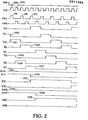
- the flip-flop circuit 10 is activated to switch the multiplexer 9 to couple the second input R to the output line 80 and a clock pulse CKL is generated on the line 95, causing the output Y2 of the shift register 4 to go low and the output Y4 of the shift register 4 to go high, as shown at 100 and 101 of Fig. 2.
- the contents of cell 11 are available at the input R of the multiplexer 9 and are transferred to the line 80 as soon as the multiplexer 9 is shifted from its left input L to its right input R .
- the flip-flop 10 switches the multiplexer 9 from its right input to its left input and a clock pulse CKR is provided on the line 96 for shifting the column shift register 5 causing the output Y3 to go low and the output Y5 to go high, as shown at 103 and 104 of Fig. 2, thereby deselecting cell 11 and selecting cell 13.
- control signal SM goes inactive (from a low to a high in this example), signaling the termination of the sequential mode and returning the memory 1 to its conventional mode.
- the initial setting of the multiplexer 9 to transfer the contents of a cell in set 19 or set 20 depends on whether the address applied to the column decoder 2 is even or odd. Accordingly, it is possible to initially set the multiplexer 9 by detecting the signal level of the least significant bit of the address applied to the inputs of the decoder 2 instead of detecting the signal levels on the output lines 30 - 33 thereof. If that is done, the circuit 8 may be eliminated. Further, while the invention as described comprises 32 memory cells, a particular embodiment of the present invention may comprise more or less than that number of memory cells. For the foregoing reasons, it is intended that the scope of the invention not be determined by reference to the embodiments described, but rather by reference to the claims hereinafter provided.
Landscapes
- Engineering & Computer Science (AREA)
- Microelectronics & Electronic Packaging (AREA)
- Static Random-Access Memory (AREA)
- Dram (AREA)
- Credit Cards Or The Like (AREA)
- Holo Graphy (AREA)
- Lubrication Of Internal Combustion Engines (AREA)
Applications Claiming Priority (2)
| Application Number | Priority Date | Filing Date | Title |
|---|---|---|---|
| US06/760,712 US4680738A (en) | 1985-07-30 | 1985-07-30 | Memory with sequential mode |
| US760712 | 1985-07-30 |
Publications (2)
| Publication Number | Publication Date |
|---|---|
| EP0211565A2 true EP0211565A2 (fr) | 1987-02-25 |
| EP0211565A3 EP0211565A3 (fr) | 1990-04-25 |
Family
ID=25059957
Family Applications (1)
| Application Number | Title | Priority Date | Filing Date |
|---|---|---|---|
| EP86305663A Withdrawn EP0211565A3 (fr) | 1985-07-30 | 1986-07-23 | Mémoires RAM |
Country Status (3)
| Country | Link |
|---|---|
| US (1) | US4680738A (fr) |
| EP (1) | EP0211565A3 (fr) |
| JP (1) | JPS6236793A (fr) |
Cited By (8)
| Publication number | Priority date | Publication date | Assignee | Title |
|---|---|---|---|---|
| EP0254886A2 (fr) * | 1986-06-30 | 1988-02-03 | Kabushiki Kaisha Toshiba | Dispositif de mémoire du type à accès séquentiel |
| FR2613570A1 (fr) * | 1987-03-30 | 1988-10-07 | Rca Licensing Corp | Correcteur d'inversion d'entrelacement pour un generateur de signaux video a image dans l'image |
| EP0315194A2 (fr) * | 1987-11-04 | 1989-05-10 | Nec Corporation | Micro-ordinateur capable d'accéder pour une courte durée à des adresses continues |
| EP0411633A2 (fr) * | 1989-08-02 | 1991-02-06 | Fujitsu Limited | Circuit de commande de conversion de balayage comprenant des mÀ©moires et un générateur d'adresses pour générer un signal d'adresse en forme de zigzag vers les mémoires |
| EP0481437A2 (fr) * | 1990-10-15 | 1992-04-22 | Kabushiki Kaisha Toshiba | Dispositif de mémoire à semi-conducteurs |
| US5798979A (en) * | 1992-03-19 | 1998-08-25 | Kabushiki Kaisha Toshiba | Clock-synchronous semiconductor memory device and access method thereof |
| US6249481B1 (en) | 1991-10-15 | 2001-06-19 | Kabushiki Kaisha Toshiba | Semiconductor memory device |
| US6310821B1 (en) | 1998-07-10 | 2001-10-30 | Kabushiki Kaisha Toshiba | Clock-synchronous semiconductor memory device and access method thereof |
Families Citing this family (21)
| Publication number | Priority date | Publication date | Assignee | Title |
|---|---|---|---|---|
| US4829471A (en) * | 1986-02-07 | 1989-05-09 | Advanced Micro Devices, Inc. | Data load sequencer for multiple data line serializer |
| US5237532A (en) * | 1986-06-30 | 1993-08-17 | Kabushiki Kaisha Toshiba | Serially-accessed type memory device for providing an interleaved data read operation |
| JPS63282997A (ja) * | 1987-05-15 | 1988-11-18 | Mitsubishi Electric Corp | ブロツクアクセスメモリ |
| NL8701392A (nl) * | 1987-06-16 | 1989-01-16 | Philips Nv | In verschillende modes schakelbare geheugeninrichting. |
| US6112287A (en) | 1993-03-01 | 2000-08-29 | Busless Computers Sarl | Shared memory multiprocessor system using a set of serial links as processors-memory switch |
| US5016216A (en) * | 1988-10-17 | 1991-05-14 | Waferscale Integration, Inc. | Decoder for a floating gate memory |
| US4985872A (en) * | 1989-06-23 | 1991-01-15 | Vlsi Technology, Inc. | Sequencing column select circuit for a random access memory |
| US4984214A (en) * | 1989-12-05 | 1991-01-08 | International Business Machines Corporation | Multiplexed serial register architecture for VRAM |
| IL96808A (en) | 1990-04-18 | 1996-03-31 | Rambus Inc | Introductory / Origin Circuit Agreed Using High-Performance Brokerage |
| US6324120B2 (en) | 1990-04-18 | 2001-11-27 | Rambus Inc. | Memory device having a variable data output length |
| US6751696B2 (en) | 1990-04-18 | 2004-06-15 | Rambus Inc. | Memory device having a programmable register |
| US5995443A (en) * | 1990-04-18 | 1999-11-30 | Rambus Inc. | Synchronous memory device |
| JP2900523B2 (ja) * | 1990-05-31 | 1999-06-02 | 日本電気株式会社 | 不揮発性半導体メモリ装置の書込回路 |
| US5285421A (en) * | 1990-07-25 | 1994-02-08 | Advanced Micro Devices | Scheme for eliminating page boundary limitation on initial access of a serial contiguous access memory |
| US5280594A (en) * | 1990-07-25 | 1994-01-18 | Advanced Micro Devices, Inc. | Architecture for high speed contiguous sequential access memories |
| US5247644A (en) * | 1991-02-06 | 1993-09-21 | Advanced Micro Devices, Inc. | Processing system with improved sequential memory accessing |
| JP3992757B2 (ja) * | 1991-04-23 | 2007-10-17 | テキサス インスツルメンツ インコーポレイテツド | マイクロプロセッサと同期するメモリ、及びデータプロセッサ、同期メモリ、周辺装置とシステムクロックを含むシステム |
| US5559990A (en) * | 1992-02-14 | 1996-09-24 | Advanced Micro Devices, Inc. | Memories with burst mode access |
| JPH05324463A (ja) * | 1992-05-18 | 1993-12-07 | Mitsubishi Electric Corp | メモリ装置及びそれを使用したデータ処理装置 |
| US6115321A (en) * | 1997-06-17 | 2000-09-05 | Texas Instruments Incorporated | Synchronous dynamic random access memory with four-bit data prefetch |
| US6240047B1 (en) | 1998-07-06 | 2001-05-29 | Texas Instruments Incorporated | Synchronous dynamic random access memory with four-bit data prefetch |
Citations (4)
| Publication number | Priority date | Publication date | Assignee | Title |
|---|---|---|---|---|
| US3930239A (en) * | 1973-07-11 | 1975-12-30 | Philips Corp | Integrated memory |
| EP0031950A2 (fr) * | 1979-12-27 | 1981-07-15 | Nec Corporation | Dispositif de mémoire |
| US4281401A (en) * | 1979-11-23 | 1981-07-28 | Texas Instruments Incorporated | Semiconductor read/write memory array having high speed serial shift register access |
| JPS58150184A (ja) * | 1982-03-02 | 1983-09-06 | Mitsubishi Electric Corp | 記憶装置 |
Family Cites Families (1)
| Publication number | Priority date | Publication date | Assignee | Title |
|---|---|---|---|---|
| US4321695A (en) * | 1979-11-23 | 1982-03-23 | Texas Instruments Incorporated | High speed serial access semiconductor memory with fault tolerant feature |
-
1985
- 1985-07-30 US US06/760,712 patent/US4680738A/en not_active Expired - Lifetime
-
1986
- 1986-07-23 EP EP86305663A patent/EP0211565A3/fr not_active Withdrawn
- 1986-07-29 JP JP61179774A patent/JPS6236793A/ja active Pending
Patent Citations (4)
| Publication number | Priority date | Publication date | Assignee | Title |
|---|---|---|---|---|
| US3930239A (en) * | 1973-07-11 | 1975-12-30 | Philips Corp | Integrated memory |
| US4281401A (en) * | 1979-11-23 | 1981-07-28 | Texas Instruments Incorporated | Semiconductor read/write memory array having high speed serial shift register access |
| EP0031950A2 (fr) * | 1979-12-27 | 1981-07-15 | Nec Corporation | Dispositif de mémoire |
| JPS58150184A (ja) * | 1982-03-02 | 1983-09-06 | Mitsubishi Electric Corp | 記憶装置 |
Non-Patent Citations (1)
| Title |
|---|
| PATENT ABSTRACTS OF JAPAN, vol. 7, no. 270 (P-240)[1415], 2nd December 1983; & JP-A-58 150 184 (MUTSIBISHI DENKI K.K.) * |
Cited By (34)
| Publication number | Priority date | Publication date | Assignee | Title |
|---|---|---|---|---|
| EP0254886A2 (fr) * | 1986-06-30 | 1988-02-03 | Kabushiki Kaisha Toshiba | Dispositif de mémoire du type à accès séquentiel |
| EP0254886B1 (fr) * | 1986-06-30 | 1993-06-16 | Kabushiki Kaisha Toshiba | Dispositif de mémoire du type à accès séquentiel |
| FR2613570A1 (fr) * | 1987-03-30 | 1988-10-07 | Rca Licensing Corp | Correcteur d'inversion d'entrelacement pour un generateur de signaux video a image dans l'image |
| EP0315194A2 (fr) * | 1987-11-04 | 1989-05-10 | Nec Corporation | Micro-ordinateur capable d'accéder pour une courte durée à des adresses continues |
| EP0315194A3 (fr) * | 1987-11-04 | 1991-02-06 | Nec Corporation | Micro-ordinateur capable d'accéder pour une courte durée à des adresses continues |
| US5313299A (en) * | 1989-08-02 | 1994-05-17 | Fujitsu Limited | Scan converter control circuit having memories and address generator for generating zigzag address signal supplied to the memories |
| EP0411633A2 (fr) * | 1989-08-02 | 1991-02-06 | Fujitsu Limited | Circuit de commande de conversion de balayage comprenant des mÀ©moires et un générateur d'adresses pour générer un signal d'adresse en forme de zigzag vers les mémoires |
| EP0411633A3 (en) * | 1989-08-02 | 1992-11-19 | Fujitsu Limited | Scan converter control circuit having memories and address generator for generating zigzag address signal supplied to the memories |
| US6373785B2 (en) | 1990-10-15 | 2002-04-16 | Kabushiki Kaisha Toshiba | Semiconductor memory device |
| US5875486A (en) * | 1990-10-15 | 1999-02-23 | Kabushiki Kaisha Toshiba | Semiconductor memory device with clock timing to activate memory cells for subsequent access |
| US5500829A (en) * | 1990-10-15 | 1996-03-19 | Kabushiki Kaisha Toshiba | Semiconductor memory device |
| US5587963A (en) * | 1990-10-15 | 1996-12-24 | Kabushiki Kaisha Toshiba | Semiconductor memory device |
| US5612925A (en) * | 1990-10-15 | 1997-03-18 | Kabushiki Kaisha Toshiba | Semiconductor memory device |
| US5737637A (en) * | 1990-10-15 | 1998-04-07 | Kabushiki Kaisha Toshiba | System for control of data I/O transfer based on cycle count in a semiconductor memory device |
| US5740122A (en) * | 1990-10-15 | 1998-04-14 | Kabushiki Kaisha Toshiba | Semiconductor memory device |
| EP0481437A3 (en) * | 1990-10-15 | 1993-07-21 | Kabushiki Kaisha Toshiba | Semiconductor memory device |
| US7158444B2 (en) | 1990-10-15 | 2007-01-02 | Kabushiki Kaisha Toshiba | Semiconductor memory device |
| US6535456B2 (en) | 1990-10-15 | 2003-03-18 | Kabushiki Kaisha Toshiba | Semiconductor memory device |
| US5926436A (en) * | 1990-10-15 | 1999-07-20 | Kabushiki Kaisha Toshiba | Semiconductor memory device |
| US7061827B2 (en) | 1990-10-15 | 2006-06-13 | Kabushiki Kaisha Toshiba | Semiconductor memory device |
| US5995442A (en) * | 1990-10-15 | 1999-11-30 | Kabushiki Kaisha Toshiba | Semiconductor memory device |
| EP0481437A2 (fr) * | 1990-10-15 | 1992-04-22 | Kabushiki Kaisha Toshiba | Dispositif de mémoire à semi-conducteurs |
| US6654314B2 (en) | 1990-10-15 | 2003-11-25 | Kabushiki Kaisha Toshiba | Semiconductor memory device |
| US6317382B2 (en) | 1990-10-15 | 2001-11-13 | Kabushiki Kaisha Toshiba | Semiconductor memory device |
| US6249481B1 (en) | 1991-10-15 | 2001-06-19 | Kabushiki Kaisha Toshiba | Semiconductor memory device |
| US5798979A (en) * | 1992-03-19 | 1998-08-25 | Kabushiki Kaisha Toshiba | Clock-synchronous semiconductor memory device and access method thereof |
| US6510101B2 (en) | 1992-03-19 | 2003-01-21 | Kabushiki Kaisha Toshiba | Clock-synchronous semiconductor memory device |
| US6639869B2 (en) | 1992-03-19 | 2003-10-28 | Kabushiki Kaisha Toshiba | Clock-synchronous semiconductor memory device |
| US6842397B2 (en) | 1992-03-19 | 2005-01-11 | Kabushiki Kaisha Toshiba | Clock-synchronous semiconductor memory device |
| US6973009B2 (en) | 1992-03-19 | 2005-12-06 | Kabushiki Kaisha Toshiba | Semiconductor memory device capable of switching between an asynchronous normal mode and a synchronous mode and method thereof |
| US5986968A (en) * | 1992-03-19 | 1999-11-16 | Kabushiki Kaisha Toshiba | Clock-synchronous semiconductor memory device and access method thereof |
| US7085193B2 (en) | 1992-03-19 | 2006-08-01 | Kabushiki Kaisha Toshiba | Clock-synchronous semiconductor memory device |
| US5818793A (en) * | 1992-03-19 | 1998-10-06 | Kabushiki Kaisha Toshiba | Clock-synchronous semiconductor memory device |
| US6310821B1 (en) | 1998-07-10 | 2001-10-30 | Kabushiki Kaisha Toshiba | Clock-synchronous semiconductor memory device and access method thereof |
Also Published As
| Publication number | Publication date |
|---|---|
| US4680738A (en) | 1987-07-14 |
| EP0211565A3 (fr) | 1990-04-25 |
| JPS6236793A (ja) | 1987-02-17 |
Similar Documents
| Publication | Publication Date | Title |
|---|---|---|
| US4680738A (en) | Memory with sequential mode | |
| US6816433B2 (en) | Synchronous dynamic random access memory for burst read/write operations | |
| EP0135940A2 (fr) | Circuit de mémoire à double porte | |
| US4740922A (en) | Semiconductor memory device having a read-modify-write configuration | |
| EP0263924A2 (fr) | Structure de réarrangement de bits sur une puce | |
| KR930014577A (ko) | 반도체 기억장치 | |
| EP0174845B1 (fr) | Dispositif de mémoire semi-conductrice | |
| EP0677189A1 (fr) | Architecture des circuits de commutation de sortie d'une memoire tampon d'image | |
| KR930024012A (ko) | 반도체 기억장치 | |
| JPS58196671A (ja) | 半導体記憶素子 | |
| JP3319637B2 (ja) | 半導体記憶装置及びその制御方法 | |
| EP0048810B1 (fr) | Réseau de mémoire à boucles récirculantes utilisant un tampon de registre à décalage | |
| JP3247639B2 (ja) | 半導体メモリ、半導体メモリのデータ読み出し方法及び書き込み方法 | |
| JPH05274862A (ja) | 半導体メモリ装置 | |
| IE53486B1 (en) | Memory | |
| EP0381940A1 (fr) | Circuit de banques de registres | |
| EP0465160B1 (fr) | Mémoire multiporte | |
| EP0285125A2 (fr) | Mémoire à semi-conducteurs avec un circuit d'entrée/de sortie parallèle | |
| JPS59180870A (ja) | 半導体記憶装置 | |
| JPH05210981A (ja) | 半導体記憶装置 | |
| JPS5930295A (ja) | 半導体メモリのアクセス方式 | |
| JPS6365516A (ja) | 走査方式 | |
| JPH0757455A (ja) | 半導体メモリ | |
| JPS6314395A (ja) | 記憶回路 | |
| JPH04117696A (ja) | 半導体メモリ装置 |
Legal Events
| Date | Code | Title | Description |
|---|---|---|---|
| PUAI | Public reference made under article 153(3) epc to a published international application that has entered the european phase |
Free format text: ORIGINAL CODE: 0009012 |
|
| AK | Designated contracting states |
Kind code of ref document: A2 Designated state(s): AT BE CH DE FR GB IT LI LU NL SE |
|
| PUAL | Search report despatched |
Free format text: ORIGINAL CODE: 0009013 |
|
| AK | Designated contracting states |
Kind code of ref document: A3 Designated state(s): AT BE CH DE FR GB IT LI LU NL SE |
|
| 17P | Request for examination filed |
Effective date: 19901004 |
|
| 17Q | First examination report despatched |
Effective date: 19910611 |
|
| STAA | Information on the status of an ep patent application or granted ep patent |
Free format text: STATUS: THE APPLICATION IS DEEMED TO BE WITHDRAWN |
|
| 18D | Application deemed to be withdrawn |
Effective date: 19920923 |
|
| RIN1 | Information on inventor provided before grant (corrected) |
Inventor name: TAM, ALOYSIUS T. |