EP0208087A2 - Elément de plastique avec voies conductrices - Google Patents
Elément de plastique avec voies conductrices Download PDFInfo
- Publication number
- EP0208087A2 EP0208087A2 EP86106454A EP86106454A EP0208087A2 EP 0208087 A2 EP0208087 A2 EP 0208087A2 EP 86106454 A EP86106454 A EP 86106454A EP 86106454 A EP86106454 A EP 86106454A EP 0208087 A2 EP0208087 A2 EP 0208087A2
- Authority
- EP
- European Patent Office
- Prior art keywords
- plastic
- conductive
- part according
- recesses
- openings
- Prior art date
- Legal status (The legal status is an assumption and is not a legal conclusion. Google has not performed a legal analysis and makes no representation as to the accuracy of the status listed.)
- Granted
Links
- 229920003023 plastic Polymers 0.000 title claims description 50
- 239000004033 plastic Substances 0.000 title claims description 49
- 238000004519 manufacturing process Methods 0.000 claims description 4
- 238000000034 method Methods 0.000 claims description 4
- 239000004020 conductor Substances 0.000 claims description 3
- 238000001746 injection moulding Methods 0.000 claims description 3
- 239000011241 protective layer Substances 0.000 claims description 3
- 239000011810 insulating material Substances 0.000 claims description 2
- 229920001169 thermoplastic Polymers 0.000 claims description 2
- 239000004416 thermosoftening plastic Substances 0.000 claims description 2
- 239000002991 molded plastic Substances 0.000 abstract 2
- 239000010410 layer Substances 0.000 description 5
- 229920002379 silicone rubber Polymers 0.000 description 4
- 238000005476 soldering Methods 0.000 description 4
- 239000000853 adhesive Substances 0.000 description 2
- 230000001070 adhesive effect Effects 0.000 description 2
- HSFWRNGVRCDJHI-UHFFFAOYSA-N alpha-acetylene Natural products C#C HSFWRNGVRCDJHI-UHFFFAOYSA-N 0.000 description 2
- 230000007797 corrosion Effects 0.000 description 2
- 238000005260 corrosion Methods 0.000 description 2
- 230000000694 effects Effects 0.000 description 2
- 238000002347 injection Methods 0.000 description 2
- 239000007924 injection Substances 0.000 description 2
- 229920001197 polyacetylene Polymers 0.000 description 2
- 230000002787 reinforcement Effects 0.000 description 2
- 239000004944 Liquid Silicone Rubber Substances 0.000 description 1
- -1 Polyethylene Polymers 0.000 description 1
- 239000004698 Polyethylene Substances 0.000 description 1
- 238000010586 diagram Methods 0.000 description 1
- 238000005553 drilling Methods 0.000 description 1
- 238000000605 extraction Methods 0.000 description 1
- 238000003780 insertion Methods 0.000 description 1
- 230000037431 insertion Effects 0.000 description 1
- 239000012212 insulator Substances 0.000 description 1
- 230000014759 maintenance of location Effects 0.000 description 1
- 229920001200 poly(ethylene-vinyl acetate) Polymers 0.000 description 1
- 239000004417 polycarbonate Substances 0.000 description 1
- 229920000515 polycarbonate Polymers 0.000 description 1
- 229920000573 polyethylene Polymers 0.000 description 1
- 229910000679 solder Inorganic materials 0.000 description 1
- 238000005507 spraying Methods 0.000 description 1
- 239000012808 vapor phase Substances 0.000 description 1
- XLYOFNOQVPJJNP-UHFFFAOYSA-N water Substances O XLYOFNOQVPJJNP-UHFFFAOYSA-N 0.000 description 1
Images
Classifications
-
- H—ELECTRICITY
- H05—ELECTRIC TECHNIQUES NOT OTHERWISE PROVIDED FOR
- H05K—PRINTED CIRCUITS; CASINGS OR CONSTRUCTIONAL DETAILS OF ELECTRIC APPARATUS; MANUFACTURE OF ASSEMBLAGES OF ELECTRICAL COMPONENTS
- H05K3/00—Apparatus or processes for manufacturing printed circuits
-
- H—ELECTRICITY
- H05—ELECTRIC TECHNIQUES NOT OTHERWISE PROVIDED FOR
- H05K—PRINTED CIRCUITS; CASINGS OR CONSTRUCTIONAL DETAILS OF ELECTRIC APPARATUS; MANUFACTURE OF ASSEMBLAGES OF ELECTRICAL COMPONENTS
- H05K3/00—Apparatus or processes for manufacturing printed circuits
- H05K3/10—Apparatus or processes for manufacturing printed circuits in which conductive material is applied to the insulating support in such a manner as to form the desired conductive pattern
- H05K3/101—Apparatus or processes for manufacturing printed circuits in which conductive material is applied to the insulating support in such a manner as to form the desired conductive pattern by casting or moulding of conductive material
-
- H—ELECTRICITY
- H01—ELECTRIC ELEMENTS
- H01B—CABLES; CONDUCTORS; INSULATORS; SELECTION OF MATERIALS FOR THEIR CONDUCTIVE, INSULATING OR DIELECTRIC PROPERTIES
- H01B1/00—Conductors or conductive bodies characterised by the conductive materials; Selection of materials as conductors
- H01B1/06—Conductors or conductive bodies characterised by the conductive materials; Selection of materials as conductors mainly consisting of other non-metallic substances
- H01B1/12—Conductors or conductive bodies characterised by the conductive materials; Selection of materials as conductors mainly consisting of other non-metallic substances organic substances
-
- B—PERFORMING OPERATIONS; TRANSPORTING
- B29—WORKING OF PLASTICS; WORKING OF SUBSTANCES IN A PLASTIC STATE IN GENERAL
- B29K—INDEXING SCHEME ASSOCIATED WITH SUBCLASSES B29B, B29C OR B29D, RELATING TO MOULDING MATERIALS OR TO MATERIALS FOR MOULDS, REINFORCEMENTS, FILLERS OR PREFORMED PARTS, e.g. INSERTS
- B29K2083/00—Use of polymers having silicon, with or without sulfur, nitrogen, oxygen, or carbon only, in the main chain, as moulding material
- B29K2083/005—LSR, i.e. liquid silicone rubbers, or derivatives thereof
-
- H—ELECTRICITY
- H05—ELECTRIC TECHNIQUES NOT OTHERWISE PROVIDED FOR
- H05K—PRINTED CIRCUITS; CASINGS OR CONSTRUCTIONAL DETAILS OF ELECTRIC APPARATUS; MANUFACTURE OF ASSEMBLAGES OF ELECTRICAL COMPONENTS
- H05K1/00—Printed circuits
- H05K1/02—Details
- H05K1/09—Use of materials for the conductive, e.g. metallic pattern
- H05K1/092—Dispersed materials, e.g. conductive pastes or inks
- H05K1/095—Dispersed materials, e.g. conductive pastes or inks for polymer thick films, i.e. having a permanent organic polymeric binder
-
- H—ELECTRICITY
- H05—ELECTRIC TECHNIQUES NOT OTHERWISE PROVIDED FOR
- H05K—PRINTED CIRCUITS; CASINGS OR CONSTRUCTIONAL DETAILS OF ELECTRIC APPARATUS; MANUFACTURE OF ASSEMBLAGES OF ELECTRICAL COMPONENTS
- H05K2201/00—Indexing scheme relating to printed circuits covered by H05K1/00
- H05K2201/09—Shape and layout
- H05K2201/09009—Substrate related
- H05K2201/09036—Recesses or grooves in insulating substrate
-
- H—ELECTRICITY
- H05—ELECTRIC TECHNIQUES NOT OTHERWISE PROVIDED FOR
- H05K—PRINTED CIRCUITS; CASINGS OR CONSTRUCTIONAL DETAILS OF ELECTRIC APPARATUS; MANUFACTURE OF ASSEMBLAGES OF ELECTRICAL COMPONENTS
- H05K2201/00—Indexing scheme relating to printed circuits covered by H05K1/00
- H05K2201/09—Shape and layout
- H05K2201/09009—Substrate related
- H05K2201/09118—Moulded substrate
-
- H—ELECTRICITY
- H05—ELECTRIC TECHNIQUES NOT OTHERWISE PROVIDED FOR
- H05K—PRINTED CIRCUITS; CASINGS OR CONSTRUCTIONAL DETAILS OF ELECTRIC APPARATUS; MANUFACTURE OF ASSEMBLAGES OF ELECTRICAL COMPONENTS
- H05K2203/00—Indexing scheme relating to apparatus or processes for manufacturing printed circuits covered by H05K3/00
- H05K2203/01—Tools for processing; Objects used during processing
- H05K2203/0104—Tools for processing; Objects used during processing for patterning or coating
- H05K2203/0113—Female die used for patterning or transferring, e.g. temporary substrate having recessed pattern
-
- H—ELECTRICITY
- H05—ELECTRIC TECHNIQUES NOT OTHERWISE PROVIDED FOR
- H05K—PRINTED CIRCUITS; CASINGS OR CONSTRUCTIONAL DETAILS OF ELECTRIC APPARATUS; MANUFACTURE OF ASSEMBLAGES OF ELECTRICAL COMPONENTS
- H05K3/00—Apparatus or processes for manufacturing printed circuits
- H05K3/10—Apparatus or processes for manufacturing printed circuits in which conductive material is applied to the insulating support in such a manner as to form the desired conductive pattern
- H05K3/107—Apparatus or processes for manufacturing printed circuits in which conductive material is applied to the insulating support in such a manner as to form the desired conductive pattern by filling grooves in the support with conductive material
-
- Y—GENERAL TAGGING OF NEW TECHNOLOGICAL DEVELOPMENTS; GENERAL TAGGING OF CROSS-SECTIONAL TECHNOLOGIES SPANNING OVER SEVERAL SECTIONS OF THE IPC; TECHNICAL SUBJECTS COVERED BY FORMER USPC CROSS-REFERENCE ART COLLECTIONS [XRACs] AND DIGESTS
- Y10—TECHNICAL SUBJECTS COVERED BY FORMER USPC
- Y10S—TECHNICAL SUBJECTS COVERED BY FORMER USPC CROSS-REFERENCE ART COLLECTIONS [XRACs] AND DIGESTS
- Y10S428/00—Stock material or miscellaneous articles
- Y10S428/901—Printed circuit
-
- Y—GENERAL TAGGING OF NEW TECHNOLOGICAL DEVELOPMENTS; GENERAL TAGGING OF CROSS-SECTIONAL TECHNOLOGIES SPANNING OVER SEVERAL SECTIONS OF THE IPC; TECHNICAL SUBJECTS COVERED BY FORMER USPC CROSS-REFERENCE ART COLLECTIONS [XRACs] AND DIGESTS
- Y10—TECHNICAL SUBJECTS COVERED BY FORMER USPC
- Y10T—TECHNICAL SUBJECTS COVERED BY FORMER US CLASSIFICATION
- Y10T428/00—Stock material or miscellaneous articles
- Y10T428/24—Structurally defined web or sheet [e.g., overall dimension, etc.]
- Y10T428/24802—Discontinuous or differential coating, impregnation or bond [e.g., artwork, printing, retouched photograph, etc.]
- Y10T428/24851—Intermediate layer is discontinuous or differential
-
- Y—GENERAL TAGGING OF NEW TECHNOLOGICAL DEVELOPMENTS; GENERAL TAGGING OF CROSS-SECTIONAL TECHNOLOGIES SPANNING OVER SEVERAL SECTIONS OF THE IPC; TECHNICAL SUBJECTS COVERED BY FORMER USPC CROSS-REFERENCE ART COLLECTIONS [XRACs] AND DIGESTS
- Y10—TECHNICAL SUBJECTS COVERED BY FORMER USPC
- Y10T—TECHNICAL SUBJECTS COVERED BY FORMER US CLASSIFICATION
- Y10T428/00—Stock material or miscellaneous articles
- Y10T428/31504—Composite [nonstructural laminate]
- Y10T428/31507—Of polycarbonate
Definitions
- the invention relates to a plastic part with electrical Stromwe g s, in particular printed circuit boards consisting of insulating and conductive materials, and a method for its production.
- Printed circuit boards made of Pertinax are known, in which electronic components are inserted with their wire ends through holes on one side, which are at least partially connected to one another on the other side with a line system made of thin metallic layers. The contact between the wire end and the line system is established by soldering when passing over a hot solder bath or using the vapor phase soldering process.
- circuit boards The disadvantage of these circuit boards is that the production of electroplated conductor tracks, the drilling of the receptacles for the components and the subsequent soldering is very expensive.
- the invention has for its object to find an economically producible plastic part with current paths, which can be equipped with reliable electrical contacts with other electrical components without the use of heat and tools, the current paths should only be indirectly accessible if necessary.
- a molded part made of insulating plastic has recesses and / or openings, in the area of which a conductive plastic is at least partially arranged as a current path.
- the molded part which can be designed as a plate or as a spatial body, serves as a support and insulator for the electrical system made of conductive plastic.
- This system consists of current paths, which lie primarily in the recesses running parallel to the surface on one or both sides, and optionally reinforcements, which are primarily arranged in the openings and depressions extending transversely to the surface.
- Components can be fitted on one or both sides, whereby a transparent plastic makes checking much easier.
- the components can be pressed directly into the reinforcements of the conductive plastic with their contact pins, whereby a secure mounting of the components and a perfect electrical contact can also be achieved over a long service life.
- the risk of corrosion due to air entry or cracks is low due to the use of elastic plastic, especially for the conductive system.
- adhesive components known as lead less components, which are distinguished by an electrically conductive adhesive connection.
- the conductivity of the conductive plastic is greater than 0.01 S / cm.
- Liquid silicone rubbers (LSR) 10 Q cm The following are suitable as conductive plastics: Liquid silicone rubbers (LSR) 10 Q cm.
- At least one of the plastics consists of injection molded thermoplastic.
- the mostly elongated recesses have a depth of 0.2-4 mm, in particular 0.8-2 mm.
- a certain cross-section is necessary to avoid high voltage losses; on the other hand, the board should not become too thick. Therefore, a depth of the recesses of 0.8-2 mm has been found to be particularly advantageous, a width of 0.5-4 mm generally being sufficient.
- the conductive plastic can completely or partially fill the recesses. Also are Current paths are conceivable in which the conductive plastic protrudes in order to obtain a larger line cross section.
- holes are provided as openings which are only partially filled with conductive plastic.
- the insertion of the contact pins can be facilitated and, if necessary, an improved retention against extraction, for example as a result of the barb effect.
- At least the conductive plastic is covered by an insulating protective layer.
- a protected against corrosion and short plastic part By spraying a third layer a protected against corrosion and short plastic part can forth wherein the outer contact pins may be forced through the insulating protective layer are e-g represents.
- plastic parts are particularly advantageous, for example, in the case of lights in vehicles which come into contact with moisture.
- a shield can also be produced by further conductive layers.
- Method for producing a plastic part with electrical current paths solved in that one of the components is injected from a conductive plastic in the form of at least one current path.
- the conductive plastic makes it possible for mass products to produce a printed circuit board, for example, only by applying it to the surface of the insulating plastic, the contacts being glued on in an electrically conductive manner or, if the thickness is large enough, pressed in.
- the conductive plastic is at least partially injected as a current path into recesses or openings in a molded part made of insulating plastic and produced by injection molding.
- the process is very economical, since several components that come from different injection molding machines can be injected one after the other into the next mold to form a uniform molded part.
- a complicated plastic part with electrical Stromwe g en and, if necessary shielding layers against water and stray field can be generated in one operation.
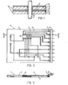
- FIG. 1 shows a cross section through a plurality of printed circuit boards 1 made of plastic, in which a molded part 2 made of insulating plastic is provided with recesses 3, into which introductory plastic is injected as current path 4. A layer 5 of insulating plastic was sprayed thereon, which carries a further molded part 2 with current path 4. A contact pin is inserted through a through hole as opening 6.
- a circuit board 1 is shown, in which a molded part 2 is provided below and above with recesses 3 which receive the current paths 4 made of conductive plastic.
- a molded part 2 is provided below and above with recesses 3 which receive the current paths 4 made of conductive plastic.
- pins 7 of a plug connector 8 are arranged in the openings.
- the molded part is injection molded from polycarbonate (Makroion® Type 2800) and has a wall thickness of 2 mm.
Landscapes
- Engineering & Computer Science (AREA)
- Manufacturing & Machinery (AREA)
- Microelectronics & Electronic Packaging (AREA)
- Physics & Mathematics (AREA)
- Spectroscopy & Molecular Physics (AREA)
- Injection Moulding Of Plastics Or The Like (AREA)
- Structure Of Printed Boards (AREA)
- Manufacturing Of Printed Wiring (AREA)
- Parts Printed On Printed Circuit Boards (AREA)
- Production Of Multi-Layered Print Wiring Board (AREA)
Applications Claiming Priority (2)
| Application Number | Priority Date | Filing Date | Title |
|---|---|---|---|
| DE19853518975 DE3518975A1 (de) | 1985-05-25 | 1985-05-25 | Kunststoffteil |
| DE3518975 | 1985-05-25 |
Publications (3)
| Publication Number | Publication Date |
|---|---|
| EP0208087A2 true EP0208087A2 (fr) | 1987-01-14 |
| EP0208087A3 EP0208087A3 (en) | 1987-05-27 |
| EP0208087B1 EP0208087B1 (fr) | 1990-06-27 |
Family
ID=6271723
Family Applications (1)
| Application Number | Title | Priority Date | Filing Date |
|---|---|---|---|
| EP86106454A Expired - Lifetime EP0208087B1 (fr) | 1985-05-25 | 1986-05-13 | Elément de plastique avec voies conductrices |
Country Status (6)
| Country | Link |
|---|---|
| US (1) | US4748068A (fr) |
| EP (1) | EP0208087B1 (fr) |
| JP (1) | JPS61276288A (fr) |
| KR (1) | KR930011601B1 (fr) |
| DE (2) | DE3518975A1 (fr) |
| ES (1) | ES8704305A1 (fr) |
Cited By (3)
| Publication number | Priority date | Publication date | Assignee | Title |
|---|---|---|---|---|
| DE19836968A1 (de) * | 1998-08-14 | 2000-02-24 | Huf Huelsbeck & Fuerst Gmbh | Elektrischer Zündanlaßschalter für Motorfahrzeuge |
| WO2012034994A1 (fr) * | 2010-09-13 | 2012-03-22 | Trw Automotive Electronics & Components Gmbh | Boîtier de commutateur pour commutateur capacitif |
| DE19955538B4 (de) * | 1999-11-18 | 2014-06-05 | Morpho Cards Gmbh | Leiterbahnträgerschicht zur Einlaminierung in eine Chipkarte, Verfahren zur Herstellung einer Leiterbahnträgerschicht Spritzgusswerkzeug zur Durchführung des Verfahrens zur Herstellung einer Leiterbahnträgerschicht |
Families Citing this family (14)
| Publication number | Priority date | Publication date | Assignee | Title |
|---|---|---|---|---|
| EP0226904A3 (fr) * | 1985-12-27 | 1989-05-24 | Hans Widmaier Fabrik für Apparate der Fernmelde- und Feinwerktechnik | Circuit imprimé, en particulier pour claviers et procédé de fabrication d'un tel circuit imprimé |
| EP0418313A4 (en) * | 1988-05-11 | 1992-01-15 | Ariel Electronics, Inc. | Circuit writer |
| US5099090A (en) * | 1988-05-11 | 1992-03-24 | Ariel Electronics, Inc. | Circuit writer |
| US5156772A (en) * | 1988-05-11 | 1992-10-20 | Ariel Electronics, Inc. | Circuit writer materials |
| US4898759A (en) * | 1988-07-27 | 1990-02-06 | Nidec Corporation | Molded printed circuit board for use with a brushless electric motor |
| DE4104853A1 (de) * | 1991-02-16 | 1992-08-20 | Standard Elektrik Lorenz Ag | Vorrichtung zur herstellung von loesbaren elektrischen verbindungen |
| EP0549791B1 (fr) * | 1991-04-01 | 1997-07-16 | Aktsionernoe obschestvo otkrytogo tipa VNIIETO | Carte de circuits imprimes multicouche et procede de fabrication |
| US5185654A (en) * | 1991-11-27 | 1993-02-09 | Motorola, Inc. | Electrostatic RF absorbant circuit carrier assembly and method for making the same |
| DE19704921C2 (de) * | 1997-02-10 | 1999-06-02 | Inotech Kunststofftechnik Gmbh | Elektronisches Bauteil |
| DE19707177A1 (de) * | 1997-02-22 | 1998-09-03 | Inotech Kunststofftechnik Gmbh | Induktivität |
| EP1245361A1 (fr) * | 2001-03-26 | 2002-10-02 | Abb Research Ltd. | Procédé de moulage par injection de pièces ayant des éléments électroconducteurs et composant électrique avec une telle pièce |
| DE102005050407A1 (de) * | 2005-10-19 | 2007-04-26 | Wilo Ag | Wickelkopfkappe mit Motorverschaltung |
| US20080191001A1 (en) * | 2007-02-08 | 2008-08-14 | Kapoor Chandaria | Packaging having protective materials incorporated therein |
| US9065213B2 (en) * | 2013-07-03 | 2015-06-23 | Tyco Electronics Corporation | Electrical connector for transmitting data signals |
Citations (5)
| Publication number | Priority date | Publication date | Assignee | Title |
|---|---|---|---|---|
| US3561110A (en) * | 1967-08-31 | 1971-02-09 | Ibm | Method of making connections and conductive paths |
| FR2402379A1 (fr) * | 1977-08-31 | 1979-03-30 | Cayrol Pierre Henri | Perfectionnements apportes aux circuits imprimes |
| GB1565207A (en) * | 1975-09-05 | 1980-04-16 | Sinclair Radionics | Printed circuits |
| GB2033667A (en) * | 1978-11-06 | 1980-05-21 | Powers C D | Improvements in circuit boards |
| EP0037988A1 (fr) * | 1980-04-11 | 1981-10-21 | Braun Aktiengesellschaft | Méthode pour appliquer des bandes électriquement conductrices sur un support en matériau isolant |
Family Cites Families (5)
| Publication number | Priority date | Publication date | Assignee | Title |
|---|---|---|---|---|
| US4295183A (en) * | 1979-06-29 | 1981-10-13 | International Business Machines Corporation | Thin film metal package for LSI chips |
| DE3021896A1 (de) * | 1980-06-06 | 1982-03-25 | Schering Ag, 1000 Berlin Und 4619 Bergkamen | Verfahren zur herstellung von gedruckten schaltungen |
| US4403107A (en) * | 1980-12-15 | 1983-09-06 | Amp Incorporated | Stamped circuit board |
| US4604799A (en) * | 1982-09-03 | 1986-08-12 | John Fluke Mfg. Co., Inc. | Method of making molded circuit board |
| US4614837A (en) * | 1985-04-03 | 1986-09-30 | Allied Corporation | Method for placing electrically conductive paths on a substrate |
-
1985
- 1985-05-25 DE DE19853518975 patent/DE3518975A1/de not_active Withdrawn
-
1986
- 1986-05-13 EP EP86106454A patent/EP0208087B1/fr not_active Expired - Lifetime
- 1986-05-13 DE DE8686106454T patent/DE3672351D1/de not_active Expired - Lifetime
- 1986-05-15 US US06/863,349 patent/US4748068A/en not_active Expired - Lifetime
- 1986-05-21 JP JP61114955A patent/JPS61276288A/ja active Pending
- 1986-05-23 ES ES555279A patent/ES8704305A1/es not_active Expired
- 1986-05-24 KR KR1019860004079A patent/KR930011601B1/ko not_active IP Right Cessation
Patent Citations (5)
| Publication number | Priority date | Publication date | Assignee | Title |
|---|---|---|---|---|
| US3561110A (en) * | 1967-08-31 | 1971-02-09 | Ibm | Method of making connections and conductive paths |
| GB1565207A (en) * | 1975-09-05 | 1980-04-16 | Sinclair Radionics | Printed circuits |
| FR2402379A1 (fr) * | 1977-08-31 | 1979-03-30 | Cayrol Pierre Henri | Perfectionnements apportes aux circuits imprimes |
| GB2033667A (en) * | 1978-11-06 | 1980-05-21 | Powers C D | Improvements in circuit boards |
| EP0037988A1 (fr) * | 1980-04-11 | 1981-10-21 | Braun Aktiengesellschaft | Méthode pour appliquer des bandes électriquement conductrices sur un support en matériau isolant |
Non-Patent Citations (2)
| Title |
|---|
| IBM TECHNICAL DISCLOSURE BULLETIN, Band 27, Nr. 5, Oktober 1984, Seiten 2937-2738, New York, US; E.W. MACE: "Subsurface circuity on polymeric substrates" * |
| IBM TECHNICAL DISCLOSURE BULLETIN, Band 27, Nr. 5, Oktober 1984, Seiten 2937-2938, New York, US; E.W. MACE: "Subsurface circuitry on polymeric substrates" * |
Cited By (5)
| Publication number | Priority date | Publication date | Assignee | Title |
|---|---|---|---|---|
| DE19836968A1 (de) * | 1998-08-14 | 2000-02-24 | Huf Huelsbeck & Fuerst Gmbh | Elektrischer Zündanlaßschalter für Motorfahrzeuge |
| DE19836968C2 (de) * | 1998-08-14 | 2002-05-08 | Huf Huelsbeck & Fuerst Gmbh | Elektrischer Zündanlaßschalter für Motorfahrzeuge |
| DE19955538B4 (de) * | 1999-11-18 | 2014-06-05 | Morpho Cards Gmbh | Leiterbahnträgerschicht zur Einlaminierung in eine Chipkarte, Verfahren zur Herstellung einer Leiterbahnträgerschicht Spritzgusswerkzeug zur Durchführung des Verfahrens zur Herstellung einer Leiterbahnträgerschicht |
| WO2012034994A1 (fr) * | 2010-09-13 | 2012-03-22 | Trw Automotive Electronics & Components Gmbh | Boîtier de commutateur pour commutateur capacitif |
| US9722603B2 (en) | 2010-09-13 | 2017-08-01 | Trw Automotive Electronics & Components Gmbh | Switch housing for capacitive switches |
Also Published As
| Publication number | Publication date |
|---|---|
| ES555279A0 (es) | 1987-03-16 |
| KR870008495A (ko) | 1987-09-26 |
| KR930011601B1 (ko) | 1993-12-13 |
| JPS61276288A (ja) | 1986-12-06 |
| EP0208087B1 (fr) | 1990-06-27 |
| DE3518975A1 (de) | 1986-11-27 |
| DE3672351D1 (de) | 1990-08-02 |
| ES8704305A1 (es) | 1987-03-16 |
| EP0208087A3 (en) | 1987-05-27 |
| US4748068A (en) | 1988-05-31 |
Similar Documents
| Publication | Publication Date | Title |
|---|---|---|
| EP0208087B1 (fr) | Elément de plastique avec voies conductrices | |
| DE69219007T2 (de) | Aktiver elektrischer Verbinder | |
| DE4021871C2 (de) | Hochintegriertes elektronisches Bauteil | |
| DE2455619A1 (de) | Steckverbinder-anordnung | |
| DE3908481A1 (de) | Elektrische abzweigdose sowie ein verfahren zur herstellung derselben | |
| DE2752438A1 (de) | Anordnung fuer das packen von monolithisch integrierten halbleiterschaltungen | |
| DE69216452T2 (de) | Halbleiteranordnung mit elektromagnetischer Abschirmung | |
| DE3007822A1 (de) | Magnetblasenvorrichtung | |
| DE60017695T2 (de) | Elektrischer Verbinderanschlusskasten | |
| DE69201274T2 (de) | Integrierschaltungsgerät mit verbesserten Pfosten für oberflächenmontiertes Gehäuse. | |
| DE4436523B4 (de) | Verfahren zur Herstellung eines elektronischen Gerätes und Drehzahlsensor mit einer elektronischen Schaltung | |
| EP1424882A1 (fr) | Câble conducteur plat | |
| DE69509110T2 (de) | Leitfähige tinte mit metallischen perlen von abweichenden schmelzpunkten | |
| DE3731413C2 (fr) | ||
| DE3829117A1 (de) | Metallkern-leiterplatte | |
| DE68923361T2 (de) | Modulares Verbindersystem mit oberflächenmontierten Verbindern hoher Kontaktelementdichte. | |
| DE4319876A1 (de) | Verfahren zum Befestigen einer Hybrid-Schaltung auf einer Leiterplatte | |
| DE69609921T2 (de) | Herstellungsverfahren einer halbleiteranordnung geeignet zur oberflächenmontage | |
| DE102010027149A1 (de) | Verbiegbare Metallkernleiterplatte | |
| DE2758826A1 (de) | Logikkarte zur verbindung integrierter schaltkreisbausteine | |
| DE68919953T2 (de) | Elektrische Komponente. | |
| DE102010041121A1 (de) | Schaltungsträger sowie Verfahren zur Herstellung eines Schaltungsträgers | |
| DE102022000860A1 (de) | Verbinder und Platteneinheit | |
| DE2257888A1 (de) | Abschlussleiste fuer steckbare bauelemente | |
| DE60218936T2 (de) | Harzgegossene Platte |
Legal Events
| Date | Code | Title | Description |
|---|---|---|---|
| PUAI | Public reference made under article 153(3) epc to a published international application that has entered the european phase |
Free format text: ORIGINAL CODE: 0009012 |
|
| 17P | Request for examination filed |
Effective date: 19860513 |
|
| AK | Designated contracting states |
Kind code of ref document: A2 Designated state(s): DE FR GB IT NL |
|
| PUAL | Search report despatched |
Free format text: ORIGINAL CODE: 0009013 |
|
| AK | Designated contracting states |
Kind code of ref document: A3 Designated state(s): DE FR GB IT NL |
|
| 17Q | First examination report despatched |
Effective date: 19890222 |
|
| GRAA | (expected) grant |
Free format text: ORIGINAL CODE: 0009210 |
|
| AK | Designated contracting states |
Kind code of ref document: B1 Designated state(s): DE FR GB IT NL |
|
| ITF | It: translation for a ep patent filed | ||
| ET | Fr: translation filed | ||
| REF | Corresponds to: |
Ref document number: 3672351 Country of ref document: DE Date of ref document: 19900802 |
|
| GBT | Gb: translation of ep patent filed (gb section 77(6)(a)/1977) | ||
| PLBE | No opposition filed within time limit |
Free format text: ORIGINAL CODE: 0009261 |
|
| STAA | Information on the status of an ep patent application or granted ep patent |
Free format text: STATUS: NO OPPOSITION FILED WITHIN TIME LIMIT |
|
| ITTA | It: last paid annual fee | ||
| 26N | No opposition filed | ||
| PGFP | Annual fee paid to national office [announced via postgrant information from national office to epo] |
Ref country code: DE Payment date: 20000413 Year of fee payment: 15 |
|
| PGFP | Annual fee paid to national office [announced via postgrant information from national office to epo] |
Ref country code: FR Payment date: 20000428 Year of fee payment: 15 |
|
| PGFP | Annual fee paid to national office [announced via postgrant information from national office to epo] |
Ref country code: GB Payment date: 20000510 Year of fee payment: 15 |
|
| PGFP | Annual fee paid to national office [announced via postgrant information from national office to epo] |
Ref country code: NL Payment date: 20000531 Year of fee payment: 15 |
|
| PG25 | Lapsed in a contracting state [announced via postgrant information from national office to epo] |
Ref country code: GB Free format text: LAPSE BECAUSE OF NON-PAYMENT OF DUE FEES Effective date: 20010513 |
|
| PG25 | Lapsed in a contracting state [announced via postgrant information from national office to epo] |
Ref country code: NL Free format text: LAPSE BECAUSE OF NON-PAYMENT OF DUE FEES Effective date: 20011201 |
|
| GBPC | Gb: european patent ceased through non-payment of renewal fee |
Effective date: 20010513 |
|
| PG25 | Lapsed in a contracting state [announced via postgrant information from national office to epo] |
Ref country code: FR Free format text: LAPSE BECAUSE OF NON-PAYMENT OF DUE FEES Effective date: 20020131 |
|
| NLV4 | Nl: lapsed or anulled due to non-payment of the annual fee |
Effective date: 20011201 |
|
| PG25 | Lapsed in a contracting state [announced via postgrant information from national office to epo] |
Ref country code: DE Free format text: LAPSE BECAUSE OF NON-PAYMENT OF DUE FEES Effective date: 20020301 |
|
| PG25 | Lapsed in a contracting state [announced via postgrant information from national office to epo] |
Ref country code: IT Free format text: LAPSE BECAUSE OF NON-PAYMENT OF DUE FEES;WARNING: LAPSES OF ITALIAN PATENTS WITH EFFECTIVE DATE BEFORE 2007 MAY HAVE OCCURRED AT ANY TIME BEFORE 2007. THE CORRECT EFFECTIVE DATE MAY BE DIFFERENT FROM THE ONE RECORDED. Effective date: 20050513 |