EP0207767B1 - Gerät und Verfahren mit gepulstem Plasma - Google Patents
Gerät und Verfahren mit gepulstem Plasma Download PDFInfo
- Publication number
- EP0207767B1 EP0207767B1 EP86305036A EP86305036A EP0207767B1 EP 0207767 B1 EP0207767 B1 EP 0207767B1 EP 86305036 A EP86305036 A EP 86305036A EP 86305036 A EP86305036 A EP 86305036A EP 0207767 B1 EP0207767 B1 EP 0207767B1
- Authority
- EP
- European Patent Office
- Prior art keywords
- plasma
- gas
- chamber
- pulse
- generator
- Prior art date
- Legal status (The legal status is an assumption and is not a legal conclusion. Google has not performed a legal analysis and makes no representation as to the accuracy of the status listed.)
- Expired
Links
Images


Classifications
-
- H—ELECTRICITY
- H01—ELECTRIC ELEMENTS
- H01J—ELECTRIC DISCHARGE TUBES OR DISCHARGE LAMPS
- H01J37/00—Discharge tubes with provision for introducing objects or material to be exposed to the discharge, e.g. for the purpose of examination or processing thereof
- H01J37/32—Gas-filled discharge tubes
- H01J37/32431—Constructional details of the reactor
- H01J37/3244—Gas supply means
-
- C—CHEMISTRY; METALLURGY
- C23—COATING METALLIC MATERIAL; COATING MATERIAL WITH METALLIC MATERIAL; CHEMICAL SURFACE TREATMENT; DIFFUSION TREATMENT OF METALLIC MATERIAL; COATING BY VACUUM EVAPORATION, BY SPUTTERING, BY ION IMPLANTATION OR BY CHEMICAL VAPOUR DEPOSITION, IN GENERAL; INHIBITING CORROSION OF METALLIC MATERIAL OR INCRUSTATION IN GENERAL
- C23C—COATING METALLIC MATERIAL; COATING MATERIAL WITH METALLIC MATERIAL; SURFACE TREATMENT OF METALLIC MATERIAL BY DIFFUSION INTO THE SURFACE, BY CHEMICAL CONVERSION OR SUBSTITUTION; COATING BY VACUUM EVAPORATION, BY SPUTTERING, BY ION IMPLANTATION OR BY CHEMICAL VAPOUR DEPOSITION, IN GENERAL
- C23C16/00—Chemical coating by decomposition of gaseous compounds, without leaving reaction products of surface material in the coating, i.e. chemical vapour deposition [CVD] processes
- C23C16/44—Chemical coating by decomposition of gaseous compounds, without leaving reaction products of surface material in the coating, i.e. chemical vapour deposition [CVD] processes characterised by the method of coating
- C23C16/50—Chemical coating by decomposition of gaseous compounds, without leaving reaction products of surface material in the coating, i.e. chemical vapour deposition [CVD] processes characterised by the method of coating using electric discharges
- C23C16/515—Chemical coating by decomposition of gaseous compounds, without leaving reaction products of surface material in the coating, i.e. chemical vapour deposition [CVD] processes characterised by the method of coating using electric discharges using pulsed discharges
Definitions
- This invention relates to apparatus and processes for pulsed plasma treatment of a substrate surface.
- Plasma processing and in particular low temperature glow discharge plasma processing, is potentially a very useful process for the surface processing of substrate materials.
- the object of the present invention is to minimise or to overcome these disadvantages.
- an apparatus for pulsed plasma processing of a substrate surface including a reactor chamber, a radio frequency pulsed generator coupled to the chamber and whereby, in use, a substantially fully dissociated plasma is generated in the chamber by each generator pulse, means for evacuating the chamber, means for controlling the supply of a plurality of gases to the chamber, and means for traversing the plasma across the substrate surface whereby, at a given instant, only part of the substrate surface is exposed to or in contact with the plasma.
- the gas supply means is adapted to admit gas to the chamber in a pulsed manner, and gas pulse corresponding to a generator pulse whereby to achieve fresh gas conditions at the commencement of each generator pulse, and that the evacuating means is adapted to remove gas from the chamber at a rate corresponding to a substantially complete gas exchange within the chamber from each successive generator pulse.
- a process for pulse plasma treatment of a substrate surface including exposing the substrate surface in a reactor chamber under reduced pressure to pulsed radio frequency energy of sufficient intensity to generate a substantially fully dissociated plasma within the chamber, and traversing said plasma across the substrate surface whereby, at a given instant, only part of the surface is exposed to or in contact with the plasma, characterised in that gases are selectively admitted to the chamber in a pulsed manner, each gas pulse corresponding to a generator pulse whereby to achieve fresh gas conditions at the commencement of each generator pulse, and that the chamber is evacuated at a rate corresponding to a substantially complete gas exchange within the chamber for each successive generator pulse.
- radio frequency as employed herein is understood to include microwave frequencies.
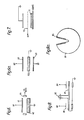
- Fig. l is a schematic diagram of an apparatus for pulsed plasma processing
- Fig. 2 is a schematic diagram of a pulse radio frequency generator
- Fig. 2a shows a modified radio frequency generator
- Fig. 3 shows the HT supply circuitry of the generation of Fig. l;
- Fig. 3a shows a protection circuit for use with the power supply of Fig. 3;
- Figs. 4a and 4b illustrate features of the gas handling system of the apparatus of Fig. l;
- Fig. 5 shows a typical gas supply sequence
- Figs. 6, 6a and 7 illustrate forms of plasma reactor
- Figs. 8 and 8a show a modified plasma reactor
- Fig. 9 shows a further plasma reactor arrangement.
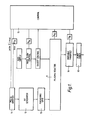
- the apparatus includes a plasma reactor ll within which a pulsed radio frequency plasma is maintained by a generator l2 and an associated impedance matching unit l3.
- the generator is driven via a pulse amplifier l4 from a central control l5, e.g. a microprocessor.
- the control l5 also controls a gas supply to the reactor ll and the rate at which the reactor is evacuated via a variable throttle l6 and a vacuum pump l7.
- the gas supply i.e. a plurality of gases or gas mixtures, is fed to the reactor via a set of mass flow controllers l8 and ON/OFF controllers l9. Coupling of the micropressor l5 to the system controls may be effected via A/D and D/A converters.
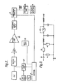
- FIG. 2 shows the preferred features of a pulsed r.f. generator.
- a pulse amplifier 2l applies a strong negative bias (e.g. -l80V) to the grid of the buffer stage valve Vl of the generator during the pulse intervals.
- a radio frequency generator includes an oscillator, a power output valve and a buffer stage therebetween.
- a signal from the microprocessor l5, or a pulse generator, reduces this bias typically to -30V during the pulse thus turning the generator ON for the duration of the pulse.
- a second input 22 to the grid may therefore be provided through which the negative bias may be varied to maintain a weak plasma in this interpulse period.
- a processor controlled bias amplifier 23 for automatic peak power control.
- this facility enables the operator to determine the appropriate impedance matching condition before full power is applied.
- a typical treatment process is started at low peak power levels using an inert gas (e.g. helium) until the automatic impedance matching unit 24 fed from the directional coupler 25 e.g. via a cable link has found its matching values. This is indicated by a minimum reflected to forward power ratio by the directional coupler circuit 25 and communicated to the processor l5.
- the peak power level may then be increased to its operating value and the inert gas changed to the operating gas.
- FIG. 2a An alternative pulsing arrangement is used in Figure 2a where the pulse generator signal is used to switch the oscillator for signal of the R.F. generator. This arrangement allows fast switching circuitry and zero voltage switching methods to be used.
- the High Tension (HT) supply circuitry of the generator is shown in Fig. 3. This circuit protects the power supply 3l against the sudden power surges at the beginning of the pulse.
- the capacitor bank C B provides the pulse energy and is charged during the OFF or interpulse period through resistor Rl.
- Rl resistor
- a l3 MHz r.f. generator nominal 25 kW
- a HT capacitor bank of 6 microfarads and a charging resistor element of 60 ohm (l kw) have been found sufficient to supply peak power up to 50 kW (l to l0% reflected power) without detectable RFI.
- Pulse widths between l0 microseconds and l0 milliseconds and pulse repetition rates between 2 and 200 Hz have been tested at 50 kW peak power without RFI problems.
- the sensing signal may be derived from either the reflected power or from the R.F. line voltage to the matching unit.
- the frequency of the generator may be between 0.l and 500 MHz, and preferably between 0.5 and 60 MHz for ease of coupling and size of coupling components.
- microwaves may be used, dependent on size and shape of the samples to be treated.
- the main requirement of the generator is its ability to deliver sufficient peak power to achieve full chemical dissociation of the reactant gases in the reactor. Measurements have shown that this requires at least l00 W/cm3 for less stable gases (e.g. silane), and at least 300 W/cm3 for stable gases such as nitrogen. For the calculation of the power requirements it is important to take into account only the volume the intense plasma occupies, and not that of the whole reactor.
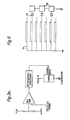
- Figures 4a and 4b show the arrangement of the gas handling components which allow rapid and controlled gas exchange manipulations.
- the arrangement differs from conventional processing techniques where a gas flow is set and the system pressure is adjusted through a throttle valve which controls the pumping speed.
- the pumping speed is closely related to the pulse repetition rate in order to achieve one gas exchange for each plasma pulse. Therefore, the gas flow rates are adjusted in order to achieve the desired partial and absolute pressures.
- These relationships are controlled through the central control unit l5 (Fig. l) in conjunction with A/D and D/A converters.
- the minimum size of the pumping stack required at a given working pressure is determined by the reactor volume times the maximum pulse repetition rate demanded by the process.
- FIG. 4 provides a facility for changing the reactant gas from one gas to another with each plasma pulse (or succession of pulses).
- Figure 4a shows a preferred gas manifold arrangement, the features of which are:
- the diameter of the common line 3l is typically between l2 and 50 mm, depending on its length.
- the inert gas at the end enables flushing of the common line at the end of each pulse.
- Other gas inlet configurations may of course be employed.
- a gas pulse facility may be provided in accordance with Fig. 4b consisting of a vessel 34 which, in operation, is charged by the mass flow controller 35 to a predetermined pressure and, at the appropriate time, discharged into the reactor chamber through the valve 32.
- the amount of gas stored in the vessel 34 should be that which fills the reactor to the required operating pressure, which pressure may change from pulse to pulse, and which is then maintained by the mass flow controller 35 during the remainder of the plasma pulse. Vessel 34 thus also acts as a buffer to prevent the mass flow controller trying to follow the pulsings.
- the volume of vessel 34 is adjusted to achieve as high a pressure for the amount of gas required as is compatible with the vapour pressure of the reactant gas which may be a liquid at elevated pressures.
- the volume may be adjusted through a piston 36 or other means.
- the gas inlet into the reactor is designed to ensure good flow randomisation without increasing the flow resistance. This may be achieved by a multitude of small angle forward deflectors. For example, in a reactor of circular cross section the gas stream may be injected tangentially to make use of the circular reactor wall for randomising the gas exchange.
- gas inlet lines are arranged in spider fashion symmetrically around the common line 3l which then acts as a mixing chamber.
- a gas handling system according to Fig. 4a was set up for the deposition of Si-N coatings in a cylindrical silica reactor of 3.5 litres total volume by sequentially admitting silane and nitrogen gas to a pressure of l6 and l0.6 Pascal (l20 mtorr and 80 mtorr) respectively.
- the pulse separation was 92 ms. Therefore the pumping speed was adjusted to l37 m3/hr. to give one gas exchange per pulse.
- the gas flows to give the desired operating pressure were 240 standard cc/min for silane and 900 standard cc/min for nitrogen. These were turned ON and OFF in anti-phase every 92 ms by means of the ON/OFF valves 32.
- the pulse vessel 34 was set to a volume of about 5 cm3 .
- the mass flow meters maintained the respective flows to charge the vessel for silane to a pressure of about 7 333 Pascal (55 torr) and that for nitrogen to about ll 333 Pascal (85 torr).
- the high valve and pipe conductance as a result of the high starting pressure allows these gases to be discharged rapidly at the beginning of the respective ON periods, thus establishing the new flow situation at each pulse very much faster than what would have been possible by the pumping speed alone.
- an argon supply connected to the inert gas line was set to a flow of 600 standard cc/min to charge vessel 34 to a pressure of about l7 332 Pascal (l30 torr). This gas was discharged for about 4 ms just before each of the other gases was turned ON. The associated pressure wave flushed and diluted all reactor parts from the previous gas, particularly in the manifold 3l.
- Figure 5 illustrates the gas pulse sequences in relation to the electrical power pulse sequences.
- Radio frequency power may be coupled to the reaction chamber by capacitive or inductive coupling or by direct coupling to electrodes disposed within the chamber.
- capacitive or inductive coupling or by direct coupling to electrodes disposed within the chamber.
- Electrodeless types include inductively coupled; capacitively coupled; and microwave cavity coupled reactors.
- Electron bombardment of the substrate when placed on the grounded electrode produces less dense, more highly stressed films.
- Typical potentials measured on the R.F. electrode during the pulse are about 2000V but this can be reduced when handling substrates (e.g. gate oxides) that are damaged by high energy ion bombardment.
- the potential may be increased by using a high voltage direct current power supply and capacitor, Bias can also be applied to the (normally grounded) counter electrode to generate a positive or negative counter bias potential.
- insulating films e.g. SiO x , SiN x
- the use of a direct current or counter bias control is inappropriate and a R.F. method must be used instead.
- the discharge initiates from the exposed electrode area and does not have time to spread uniformly over the substrate. This leads to variation of thickness and quantity of film over the substrate. This can be reduced by placing a metal ring around the electrode area and biasing it negative either using a direct current generator or a R.F. generator. The ring repels electrons towards the centre of the electrode and speeds up the formation of the discharge.
- the intense plasma regime produced during the high power pulse be in contact with, or immediately adjacent, the sample surface. This is essential in order to avoid interference from polyatomic and polymeric species which are always present in significant amounts in weaker plasma regimes.
- the intense plasma is contained in a region about lcm in thickness.
- the intense plasma region may be directed towards the sample surface by means of suitably shaped reactor walls or inserts. This technique is more fully described in EP-A-0l849l7, state of the art according to Article 54(3)EPC.
- Fig. 6 shows the driven electrode 6l in close proximity (typically l0 to 20 mm) to the flat sample surface 62.
- Fig. 6a shows a similar arrangement for two-sided treatment wherein the sample 62a is supported between the electrodes 63. Magnetic fields may be used for enhanced electron trapping near the electrodes and around the reactor walls.
- the sample 7l is placed in a plasma free zone immediately under the intense plasma next to the driven grid electrode 72.
- the ion energy can be varied.
- Metal samples may be connected directly to the driven electrode. Such an arrangement is particularly advantageous for wire structures which become completely surrounded by the intense plasma.
- wire mesh structures may be coated uniformly with a wear resistant and antistick TiN layer.
- the largest area that may be treated in a single electrode operation depends on the available generator power. Typically, for a 200 kW generator this area may be up to about 600 cm2.
- the simplest form of scaling up the process is to add a cassette to cassette loading facility and to process individual areas or samples sequentially in a single pump down. This may, however, become uneconomic both in process time and generator utilization if low duty cycles have to be used, for example, in order to maintain a low sample temperature. In this case a scanning or 'raster' process allows increased pulse rates to be used.
- Two types of scanning may be distinguished, one where the treated area and the high intensity plasma regime are mechanically moved with respect to each other, and another where scanning is provided by switching the r.f. power between a plurality of electrodes.
- Fig. 8 shows a parallel plate reactor modified for pulsed operation.
- a conductive or insulating plasma shield 8l on a rotatable shaft 82 is mounted close to the drive electrode 83, preferably in the plasma dark space.
- a sector-shape opening in the shield is lined with magnets 85 which provide a magnetic field across the opening. With r.f. power applied the magnetic field acts as an electron trap and effects striking and intensifying a local high intensity plasma in the slot.
- Figure 8 shows an increasing cross-section towards the periphery of the shield which serves to compensate for the increased width of the opening.
- magnets with an increasing field strength towards the periphery may be used in order to achieve a uniform radial plasma density.
- the shield (and with it the plasma) is rotated at a rate equal to that pulse repetition rate which would be used for a stationary plasma, and the pumping speed is matched to provide one gas exchange per revolution of the shield.
- the plasma is pulsed at a rate in accordance with the number of sectors of the intense plasma which would fill the complete circle, that is such that each part of the area passed by the slot has seen one plasma pulse in each revolution of the shield.
- a parallel plate reactor of l00 cm diameter had an electrode and sample area described by 85 cm outer diameter and 35 cm inner diameter.
- a shield of the same dimensions was mounted on a drive shaft through the lid of the reactor vessel.
- the shield had a sector shaped opening lined with magnets which, in operation, produced a plasma sector of about 5° subtended angle and about 25 cm long.
- the theoretical pulse repetition rate was 72 per revolution, in practice it varies between 70 and 80 per revolution to obtain a uniform coating thickness.
- a 40 kW peak power at l3.54 MHz was used which provided up to more than 500 W/cm3 in the plasma sector.
- the gas exchange rate for the reactor was about 5 per second, using a pump stack of nominally 3000 m3/hr pumping speed. A pulse repetition rate of 360 Hz (about every 3 ms) was used and the drive speed for the shield was 300 rpm. Pulse triggering was controlled by a feedback circuit between the drive shaft and the pulse generator.
- the samples can be rotated across a stationary intense plasma produced by a sector-shaped electrode.
- a magnetic field may be used to assist confinement of the plasma.
- the spacing between the electrode and the sample surfaces must not exceed 20 mm, and preferably is between 5 and l5 mm.
- the electrode requires good water cooling since the average power is very high.
- Rotating drums may be treated using a single electrode, or using a second drum if the drums are electrically conductive. Magnetic confinement may again be used. Reactor dimensioning and operating conditions are essentially the same as those previously described with one gas exchange for each drum revolution.
- Drum electrodes may also be used for coating tapes in a reel to reel fashion. In this case two types of operation are possible:
- the pulsed r.f. power may be scanned along a sequence of electrodes.
- the principle is shown in Fig. 9.
- Each electrode 9l is connected, through suitable matching components 92, to an electronic power switch 93 which is operated by an appropriate signal from the microprocessor control unit (Fig. l).
- the electrodes are turned ON and OFF in succession with each r.f. power pulse thereby moving the plasma regime across the area covered by the electrodes.
- the electronic power switches are operated only between pulses, that is they function only as circuit breakers and are not required to actually switch r.f. power.
- the apparatus described herein can be used in a wide variety of applications. In particular it may be used for deposition of a layered or homogeneous structure using a pulsed gas sequence synchronised with the RF pulses.
- a pulsed gas sequence synchronised with the RF pulses.
- an alternating gas sequence of silane and nitrogen may be used to provide a silicon nitride film.
- one gas may be used to deposit a solid material whilst the other reacts with the deposited material.
- the solid depositing gas pressure is adjusted typically to give a film thickness of 0.3 to l monolayer per pulse.
- the pressure of the reacting gas should be significantly greater as the surface reaction may be slow.
- the solid depositing gas may be a hydride, halide, carbonyl or an organo compound of a solid element.
- the reactant gas may comprise e.g. nitrogen, oxygen or carbon dioxide.
- two solid depositing gases may be alternated to provide a multilayer structure, the gas pressures being adjusted to provide one monolayer per radio frequency pulse.
- the process can also be used for the deposition of dielectric refractory films e.g. of Si3N4, TiO2, Al2O3, BN, SiO2, B4C.
- dielectric refractory films e.g. of Si3N4, TiO2, Al2O3, BN, SiO2, B4C.
- Other refractory films include SiC, WC, TiC, TiN and BP.
- Stable TiN x films were prepared at room temperature using the pulsed gas/pulsed plasma technique using titanium tetrachloride as a precursor.
- Conventional continuous plasma films are unstable due to the large amount of chlorine present.
- the films were deposited by discharging at a pressure of 0,l333 mbar (0.l torr) mixtures of TiCl4 (30 sec/m) and N2 (500 sec/m) in one pulse and using a second pulse of N2 to abstract chlorine from the growing film.
- the pulse width was kept long (300 microseconds) so as to fully dissociate the N2 molecules so the resultant atoms could abstract chlorine from the films. It is also important to ensure that the resulting products are pumped away before allowing a fresh film layer to be formed from a Ticl4/N2 discharge.
- TiO x films cannot be formed from CO2 or O2 and TiCl4 directly using the technique of Example I due to oxygen atoms being inefficient at removing chlorine from the films.
- pulse sequence at a power of 0,l333 mbar (0.l torr):
- the amount of nitrogen inclusion can be further reduced by further pulses of CO2.
- Aluminium carbide was formed by discharging trimethyl aluminium (20 scc/m) in argon (300 scc/m) at a pressure of 0,l333 mbar (0.l torr). Aluminium oxide was produced by depositing a layer of aluminium carbide as above and oxidizing the film in a second pulse of CO2 (500 scc/m).
- Dielectric multilayer optical filters of both the reflection and transmission type were deposited.
- up to 4l layers of ⁇ /4 optical thickness of alternating SiN x (270-l200 ⁇ , n ⁇ or l.8-2.0) and SiO x (350-l400 ⁇ , n ⁇ l.4-l.5) were deposited onto glasses and plastic substrates, to form reflection filters with wavelengths in the IR, optical and UV regions of the spectrum.
- the individual SiO x layers were deposited from silane and carbon dioxide with the flow of SiN4 interrupted for every other RF pulse to obtain high optical transmission SiO x .
- the RF power was 40kW at l3.56 MHz and the pulse width was l00 microseconds with a prf of 30Hz.
- the SiN layers were deposited under similar conditions but with N2 replacing CO2, with both gases (GiH4 and N2) flaming continuously, and with a 200 microsecond pulse width (since N2 has a lower dissociation rate than CO2).
- the technique can also be used for etching.
- the bias voltage on the ground electrode was varied in the region 0 to -500 VDC to obtain an enhanced plasma which increased the etch rate of SiO whilst decreasing the resist degradation on a patterned Si wafer.
- the apparatus can be used in the deposition of transparent conductive films, e.g. for the electrodes of liquid crystal displays, and in the epitaxial deposition of elemental or compound semiconductors.
- the deposited films may be doped with one or more further materials.
- the deposited films may be used in optical applications, e.g. interference filters, anti-reflection coatings, beam splitters, polarisers and colour correction filters. Further applications include the formation of superlattices and low dimensional solids.
- Etchants such as chlorocarbonyl or chlorine/carbonmonoxide mixtures, may be used in this way e.g. for the etching of platinum, palladium or gold.
- liquid reactants e.g. TiCl4 or BCl
- an atomiser This facilitates dispersion of the reactant in the chamber and increases the rate at which such reactants are admitted.
- an ultrasonic atomiser is used for this purpose.
- the technique can be used for sputtering material from an electrode surface on to a substrate.
Claims (12)
- Vorrichtung zur Bearbeitung einer Substratoberfläche mit einem impulsförmigen Plasma, wobei die Vorrichtung eine Reaktionskammer, einen impulsgesteuerten Hochfrequenzgenerator, der mit der Kammer gekoppelt ist, wodurch im Betrieb durch jeden Generatorimpuls in der Kammer ein im wesentlichen vollständig dissoziiertes Plasma erzeugt wird, Einrichtungen zur Evakuierung der Kammer, Einrichtungen zur Steuerung der Zuführung einer Vielzahl von Gasen an die Kammer und Einrichtungen zum Bewegen des Plasmas über die Substratoberfläche hinweg einschließt, wodurch zu einem vorgegebenen Zeitpunkt lediglich ein Teil der Substratoberfläche dem Plasma ausgesetzt ist oder mit diesem in Berührung steht, dadurch gekennzeichnet, daß die Gaszuführungseinrichtung so ausgebildet ist, daß sie Gas in die Kammer in impulsförmiger Weise eintreten läßt, wobei jeder Gasimpuls einem Generatorimpuls entspricht, wodurch frische Gasbedingungen zu Beginn jedes Generatorimpulses erzielt werden, und daß die Evakuierungseinrichtungen so ausgebildet sind, daß Gas aus der Kammer mit einer Rate entfernt wird, die einem im wesentlichen vollständigen Gasaustausch in der Kammer für jeden der aufeinanderfolgenden Generatorimpulse entspricht.
- Vorrichtung nach Anspruch 1, dadurch gekennzeichnet, daß die Gaszuführungseinrichtung so ausgebildet ist, daß der Kammer ein unterschiedliches Gas für jeden aufeinanderfolgenden Plasmaimpuls zugeführt wird.
- Vorrichtung nach Anspruch 1 oder 2, dadurch gekennzeichnet, daß die Hochfrequenzimpulse aufeinanderfolgend einer Vielzahl von Elektroden zugeführt werden.
- Vorrichtung nach Anspruch 2, dadurch gekennzeichnet, daß die Gaszuführungseinrichtung so ausgebildet ist, daß sie der Kammer Impulse eines Reaktionsgases abwechselnd mit Impulsen eines inaktiven Gases zuführt.
- Verfahren zur Behandlung einer Substratoberfläche mit impulsförmigem Plasma, wobei das Verfahren das Beaufschlagen der Substratoberfläche in einer Reaktionskammer unter verringertem Druck mit impulsförmiger Hochfrequenzenergie mit ausreichender Intensität zur Erzeugung eines im wesentlichen vollständig dissoziierten Plasmas in der Kammer und des Hinwegbewegens des Plasmas über die Substratoberfläche einschließt, wodurch zu einem vorgegebenen Zeitpunkt lediglich ein Teil der Oberfläche dem Plasma ausgesetzt ist oder mit diesem in Berührung steht, dadurch gekennzeichnet, daß Gase selektiv der Kammer in impulsförmiger Weise zugeführt werden, wobei jeder Gasimpuls einem Generatorimpuls entspricht, wodurch frische Gasbedingungen zu Beginn jedes Generatorimpulses erzielt werden, und daß die Kammer mit einer Rate evakuiert wird, die einem im wesentlichen vollständigen Gasaustausch in der Kammer für jeden der aufeinanderfolgenden Generatorimpulse entspricht.
- Verfahren nach Anspruch 5, dadurch gekennzeichnet, daß eine Spitzen-Leistungsdichte von 100 bis 1000 Watt/cm³ dem Plasma zugeführt wird.
- Verfahren nach Anspruch 6, dadurch gekennzeichnet, daß eine mittlere Leistungsdichte von 0,5 bis 10 Watt/cm³ dem Plasma zugeführt wird.
- Verfahren nach Anspruch 5, 6 oder 7, dadurch gekennzeichnet, daß die Substratoberfläche so behandelt wird, daß auf ihr eine geschichtete Struktur abgeschieden wird.
- Verfahren nach einem der Ansprüche 5 bis 8, dadurch gekennzeichnet, daß eine harte Grenzfläche zwischen den Schichten geschaffen wird.
- Verfahren nach einem der Ansprüche 5 bis 9, dadurch gekennzeichnet, daß die Zusammensetzung des Plasmas bei jedem der aufeinanderfolgenden Generatorimpulse geändert wird.
- Verfahren nach einem der Ansprüche 5 bis 10, dadurch gekennzeichnet, daß das Substrat auf einer Elektrode befestigt wird, dem die Hochfrequenzimpulse zugeführt werden.
- Verfahren nach Anspruch 11, dadurch gekennzeichnet, daß die Elektrode einer Gleich-Vorspannung ausgesetzt wird.
Applications Claiming Priority (2)
| Application Number | Priority Date | Filing Date | Title |
|---|---|---|---|
| GB8516537 | 1985-06-29 | ||
| GB858516537A GB8516537D0 (en) | 1985-06-29 | 1985-06-29 | Pulsed plasma apparatus |
Publications (3)
| Publication Number | Publication Date |
|---|---|
| EP0207767A2 EP0207767A2 (de) | 1987-01-07 |
| EP0207767A3 EP0207767A3 (en) | 1989-02-08 |
| EP0207767B1 true EP0207767B1 (de) | 1991-03-13 |
Family
ID=10581562
Family Applications (1)
| Application Number | Title | Priority Date | Filing Date |
|---|---|---|---|
| EP86305036A Expired EP0207767B1 (de) | 1985-06-29 | 1986-06-27 | Gerät und Verfahren mit gepulstem Plasma |
Country Status (5)
| Country | Link |
|---|---|
| US (1) | US4935661A (de) |
| EP (1) | EP0207767B1 (de) |
| JP (1) | JPS6250472A (de) |
| DE (1) | DE3678048D1 (de) |
| GB (2) | GB8516537D0 (de) |
Families Citing this family (119)
| Publication number | Priority date | Publication date | Assignee | Title |
|---|---|---|---|---|
| DE3800712A1 (de) * | 1988-01-13 | 1989-07-27 | Philips Patentverwaltung | Verfahren zur plasmaaktivierten reaktiven abscheidung von elektrisch leitendem mehrkomponentenmaterial aus einer gasphase |
| DE3841730C2 (de) * | 1988-12-10 | 1997-06-19 | Widia Gmbh | Verfahren zum Beschichten eines metallischen Grundkörpers mit einem nichtleitenden Beschichtungsmaterial |
| US5227202A (en) * | 1989-09-22 | 1993-07-13 | Balzers Aktiengesellschaft | Method for chemical coating on opposite surfaces of workpieces |
| DE3931713C1 (de) * | 1989-09-22 | 1991-03-14 | Balzers Ag, Balzers, Li | |
| DE3933900A1 (de) * | 1989-10-11 | 1991-04-18 | Philips Patentverwaltung | Verfahren zur plasmaaktivierten reaktiven abscheidung von elektrisch leitendem mehrkomponentenmaterial aus einer gasphase |
| US5170098A (en) * | 1989-10-18 | 1992-12-08 | Matsushita Electric Industrial Co., Ltd. | Plasma processing method and apparatus for use in carrying out the same |
| JP2970916B2 (ja) * | 1989-10-19 | 1999-11-02 | 科学技術振興事業団 | ディジタルcvd方法 |
| JP2687966B2 (ja) | 1990-08-20 | 1997-12-08 | 富士通株式会社 | 半導体装置の製造方法 |
| US5273609A (en) * | 1990-09-12 | 1993-12-28 | Texas Instruments Incorporated | Method and apparatus for time-division plasma chopping in a multi-channel plasma processing equipment |
| KR930011413B1 (ko) * | 1990-09-25 | 1993-12-06 | 가부시키가이샤 한도오따이 에네루기 겐큐쇼 | 펄스형 전자파를 사용한 플라즈마 cvd 법 |
| US5305178A (en) * | 1991-08-12 | 1994-04-19 | The United States Of America As Represented By The Secretary Of The Army | Capacitor with increased electrical breakdown strength and method of forming the same |
| DE4127504A1 (de) * | 1991-08-20 | 1993-02-25 | Leybold Ag | Einrichtung zur unterdrueckung von lichtboegen |
| US5302882A (en) * | 1991-09-09 | 1994-04-12 | Sematech, Inc. | Low pass filter for plasma discharge |
| DE59209786D1 (de) * | 1991-09-20 | 2000-02-03 | Balzers Hochvakuum | Verfahren zur Schutzbeschichtung von Substraten sowie Beschichtungsanlage |
| DE4137606C1 (de) * | 1991-11-15 | 1992-07-30 | Schott Glaswerke, 6500 Mainz, De | |
| JPH05148654A (ja) * | 1991-11-28 | 1993-06-15 | Shinko Seiki Co Ltd | パルスプラズマcvdによる成膜方法及びその装置 |
| US5175472A (en) * | 1991-12-30 | 1992-12-29 | Comdel, Inc. | Power monitor of RF plasma |
| US5523955A (en) * | 1992-03-19 | 1996-06-04 | Advanced Energy Industries, Inc. | System for characterizing AC properties of a processing plasma |
| US5325019A (en) * | 1992-08-21 | 1994-06-28 | Sematech, Inc. | Control of plasma process by use of harmonic frequency components of voltage and current |
| US5334423A (en) * | 1993-01-28 | 1994-08-02 | United Solar Systems Corp. | Microwave energized process for the preparation of high quality semiconductor material |
| US5344792A (en) * | 1993-03-04 | 1994-09-06 | Micron Technology, Inc. | Pulsed plasma enhanced CVD of metal silicide conductive films such as TiSi2 |
| FR2708624A1 (fr) * | 1993-07-30 | 1995-02-10 | Neuville Stephane | Procédé de dépôt d'un revêtement protecteur à base de pseudo carbone diamant amorphe ou de carbure de silicium modifié. |
| WO1995026427A1 (de) * | 1994-03-29 | 1995-10-05 | Schott Glaswerke | Pcvd-verfahren und vorrichtung zur beschichtung von gewölbten substraten |
| JPH0892765A (ja) * | 1994-09-22 | 1996-04-09 | Tokyo Electron Ltd | エッチング方法 |
| US5983828A (en) * | 1995-10-13 | 1999-11-16 | Mattson Technology, Inc. | Apparatus and method for pulsed plasma processing of a semiconductor substrate |
| US6794301B2 (en) | 1995-10-13 | 2004-09-21 | Mattson Technology, Inc. | Pulsed plasma processing of semiconductor substrates |
| US6253704B1 (en) * | 1995-10-13 | 2001-07-03 | Mattson Technology, Inc. | Apparatus and method for pulsed plasma processing of a semiconductor substrate |
| US6030902A (en) | 1996-02-16 | 2000-02-29 | Micron Technology Inc | Apparatus and method for improving uniformity in batch processing of semiconductor wafers |
| KR0183844B1 (ko) * | 1996-04-30 | 1999-05-15 | 김광호 | 알에프 발생 장치 및 이를 이용한 펄스 플라즈마 형성 방법 |
| US6342277B1 (en) * | 1996-08-16 | 2002-01-29 | Licensee For Microelectronics: Asm America, Inc. | Sequential chemical vapor deposition |
| US5849628A (en) | 1996-12-09 | 1998-12-15 | Micron Technology, Inc. | Method of producing rough polysilicon by the use of pulsed plasma chemical vapor deposition and products produced by same |
| US6379576B2 (en) | 1997-11-17 | 2002-04-30 | Mattson Technology, Inc. | Systems and methods for variable mode plasma enhanced processing of semiconductor wafers |
| US6294466B1 (en) | 1998-05-01 | 2001-09-25 | Applied Materials, Inc. | HDP-CVD apparatus and process for depositing titanium films for semiconductor devices |
| US6185839B1 (en) * | 1998-05-28 | 2001-02-13 | Applied Materials, Inc. | Semiconductor process chamber having improved gas distributor |
| US5985375A (en) * | 1998-09-03 | 1999-11-16 | Micron Technology, Inc. | Method for pulsed-plasma enhanced vapor deposition |
| US6263829B1 (en) | 1999-01-22 | 2001-07-24 | Applied Materials, Inc. | Process chamber having improved gas distributor and method of manufacture |
| DE19911046B4 (de) * | 1999-03-12 | 2006-10-26 | Robert Bosch Gmbh | Plasmaverfahren |
| KR100273473B1 (ko) * | 1999-04-06 | 2000-11-15 | 이경수 | 박막 형성 방법 |
| EP1125321B1 (de) * | 1999-06-19 | 2007-08-15 | ASM Genitech Korea Ltd. | Chemischer abscheidereaktor und dessen verwendung für die abscheidung eines dünnen films |
| DE19933842A1 (de) * | 1999-07-20 | 2001-02-01 | Bosch Gmbh Robert | Vorrichtung und Verfahren zum Ätzen eines Substrates mittels eines induktiv gekoppelten Plasmas |
| DE60041341D1 (de) | 1999-08-17 | 2009-02-26 | Tokyo Electron Ltd | Gepulstes plasmabehandlungsverfahren und vorrichtung |
| US6511539B1 (en) | 1999-09-08 | 2003-01-28 | Asm America, Inc. | Apparatus and method for growth of a thin film |
| JP4592867B2 (ja) * | 2000-03-27 | 2010-12-08 | 株式会社半導体エネルギー研究所 | 平行平板形プラズマcvd装置及びドライクリーニングの方法 |
| US6451390B1 (en) | 2000-04-06 | 2002-09-17 | Applied Materials, Inc. | Deposition of TEOS oxide using pulsed RF plasma |
| EP2293322A1 (de) * | 2000-06-08 | 2011-03-09 | Genitech, Inc. | Verfahren zur Abscheidung einer Metallnitridschicht |
| DE10029905A1 (de) * | 2000-06-17 | 2002-01-03 | Schott Auer Gmbh | Reflektor, insbesondere zur Anwendung bei einem Kraftfahrzeug |
| US6784108B1 (en) * | 2000-08-31 | 2004-08-31 | Micron Technology, Inc. | Gas pulsing for etch profile control |
| EP1421606A4 (de) * | 2001-08-06 | 2008-03-05 | Genitech Co Ltd | Geräte für die plasmaverstärkte atomische schichtablagerung (peald) und verfahren zur bildung eines dünnen leitfähigen films damit dafür |
| US6676760B2 (en) | 2001-08-16 | 2004-01-13 | Appiled Materials, Inc. | Process chamber having multiple gas distributors and method |
| JP4763235B2 (ja) * | 2001-08-29 | 2011-08-31 | 東京エレクトロン株式会社 | プラズマ処理のための装置並びに方法 |
| US9708707B2 (en) * | 2001-09-10 | 2017-07-18 | Asm International N.V. | Nanolayer deposition using bias power treatment |
| WO2003025243A2 (en) * | 2001-09-14 | 2003-03-27 | Asm International N.V. | Metal nitride deposition by ald using gettering reactant |
| KR100760291B1 (ko) * | 2001-11-08 | 2007-09-19 | 에이에스엠지니텍코리아 주식회사 | 박막 형성 방법 |
| JP4177259B2 (ja) * | 2001-11-27 | 2008-11-05 | 東京エレクトロン株式会社 | プラズマ処理装置 |
| TWI278532B (en) * | 2002-06-23 | 2007-04-11 | Asml Us Inc | Method for energy-assisted atomic layer deposition and removal |
| KR100480914B1 (ko) * | 2002-08-05 | 2005-04-07 | 주식회사 하이닉스반도체 | 반도체소자의 캐패시터 제조방법 |
| US6924235B2 (en) * | 2002-08-16 | 2005-08-02 | Unaxis Usa Inc. | Sidewall smoothing in high aspect ratio/deep etching using a discrete gas switching method |
| US7511443B2 (en) * | 2002-09-26 | 2009-03-31 | Barrett Technology, Inc. | Ultra-compact, high-performance motor controller and method of using same |
| US7713592B2 (en) | 2003-02-04 | 2010-05-11 | Tegal Corporation | Nanolayer deposition process |
| US9121098B2 (en) | 2003-02-04 | 2015-09-01 | Asm International N.V. | NanoLayer Deposition process for composite films |
| US6829056B1 (en) | 2003-08-21 | 2004-12-07 | Michael Barnes | Monitoring dimensions of features at different locations in the processing of substrates |
| JP4483231B2 (ja) * | 2003-08-27 | 2010-06-16 | ソニー株式会社 | 磁気メモリ装置の製造方法 |
| US7405143B2 (en) * | 2004-03-25 | 2008-07-29 | Asm International N.V. | Method for fabricating a seed layer |
| US20050241762A1 (en) * | 2004-04-30 | 2005-11-03 | Applied Materials, Inc. | Alternating asymmetrical plasma generation in a process chamber |
| US20060045822A1 (en) | 2004-09-01 | 2006-03-02 | Board Of Regents, The University Of Texas System | Plasma polymerization for encapsulating particles |
| US7966969B2 (en) * | 2004-09-22 | 2011-06-28 | Asm International N.V. | Deposition of TiN films in a batch reactor |
| EP1805886B8 (de) * | 2004-09-30 | 2019-03-13 | Barrett Technology, LLC | Ultrakompakter, hochleistungsfähiger motorregler und verfahren zu seiner benutzung |
| US7427571B2 (en) * | 2004-10-15 | 2008-09-23 | Asm International, N.V. | Reactor design for reduced particulate generation |
| US7674726B2 (en) | 2004-10-15 | 2010-03-09 | Asm International N.V. | Parts for deposition reactors |
| CN100595973C (zh) * | 2005-03-30 | 2010-03-24 | 松下电器产业株式会社 | 传输线对和传输线组 |
| US8099059B2 (en) * | 2005-04-29 | 2012-01-17 | Koninklijke Philips Electronics N.V. | Method and circuit arrangement for operating multi-channel transmit/recieve antenna devices |
| US8993055B2 (en) | 2005-10-27 | 2015-03-31 | Asm International N.V. | Enhanced thin film deposition |
| US7553516B2 (en) * | 2005-12-16 | 2009-06-30 | Asm International N.V. | System and method of reducing particle contamination of semiconductor substrates |
| CN101460659B (zh) * | 2006-06-02 | 2011-12-07 | 应用材料股份有限公司 | 利用压差测量的气流控制 |
| US7691757B2 (en) | 2006-06-22 | 2010-04-06 | Asm International N.V. | Deposition of complex nitride films |
| US8268409B2 (en) * | 2006-10-25 | 2012-09-18 | Asm America, Inc. | Plasma-enhanced deposition of metal carbide films |
| US7611751B2 (en) | 2006-11-01 | 2009-11-03 | Asm America, Inc. | Vapor deposition of metal carbide films |
| EP1936656A1 (de) * | 2006-12-21 | 2008-06-25 | Nederlandse Organisatie voor Toegepast-Natuuurwetenschappelijk Onderzoek TNO | Plasmagenerator und Reinigungsverfahren für ein Objekt |
| US7595270B2 (en) * | 2007-01-26 | 2009-09-29 | Asm America, Inc. | Passivated stoichiometric metal nitride films |
| US7598170B2 (en) * | 2007-01-26 | 2009-10-06 | Asm America, Inc. | Plasma-enhanced ALD of tantalum nitride films |
| US7737042B2 (en) | 2007-02-22 | 2010-06-15 | Applied Materials, Inc. | Pulsed-plasma system for etching semiconductor structures |
| US7718538B2 (en) * | 2007-02-21 | 2010-05-18 | Applied Materials, Inc. | Pulsed-plasma system with pulsed sample bias for etching semiconductor substrates |
| US7771606B2 (en) * | 2007-02-22 | 2010-08-10 | Applied Materials, Inc. | Pulsed-plasma system with pulsed reaction gas replenish for etching semiconductors structures |
| US7713874B2 (en) * | 2007-05-02 | 2010-05-11 | Asm America, Inc. | Periodic plasma annealing in an ALD-type process |
| US7629256B2 (en) * | 2007-05-14 | 2009-12-08 | Asm International N.V. | In situ silicon and titanium nitride deposition |
| AT504487B1 (de) * | 2007-06-13 | 2008-06-15 | Ulrich Dipl Ing Dr Traxlmayr | Vorrichtung zur erzeugung von plasma oder radikalen mittels mikrowellen |
| US7453191B1 (en) * | 2007-07-06 | 2008-11-18 | Uion Co., Ltd. | Induction concentration remote atmospheric pressure plasma generating apparatus |
| US20090035946A1 (en) * | 2007-07-31 | 2009-02-05 | Asm International N.V. | In situ deposition of different metal-containing films using cyclopentadienyl metal precursors |
| KR20090018290A (ko) * | 2007-08-17 | 2009-02-20 | 에이에스엠지니텍코리아 주식회사 | 증착 장치 |
| KR20100126337A (ko) * | 2008-01-30 | 2010-12-01 | 어플라이드 머티어리얼스, 인코포레이티드 | 표면파 런칭 플라즈마 방전 소스들의 사전-이온화를 위한 시스템 및 방법 |
| US8088451B2 (en) | 2008-03-13 | 2012-01-03 | Board Of Regents, The University Of Texas System | Covalently functionalized particles for synthesis of new composite materials |
| WO2009129332A2 (en) | 2008-04-16 | 2009-10-22 | Asm America, Inc. | Atomic layer deposition of metal carbide films using aluminum hydrocarbon compounds |
| US8383525B2 (en) * | 2008-04-25 | 2013-02-26 | Asm America, Inc. | Plasma-enhanced deposition process for forming a metal oxide thin film and related structures |
| US7666474B2 (en) | 2008-05-07 | 2010-02-23 | Asm America, Inc. | Plasma-enhanced pulsed deposition of metal carbide films |
| KR101436564B1 (ko) * | 2008-05-07 | 2014-09-02 | 한국에이에스엠지니텍 주식회사 | 비정질 실리콘 박막 형성 방법 |
| US7833906B2 (en) | 2008-12-11 | 2010-11-16 | Asm International N.V. | Titanium silicon nitride deposition |
| US8659335B2 (en) | 2009-06-25 | 2014-02-25 | Mks Instruments, Inc. | Method and system for controlling radio frequency power |
| WO2011146077A1 (en) * | 2010-05-21 | 2011-11-24 | Board Of Regents, The University Of Texas System | Encapsulated particles for amorphous stability enhancement |
| DE202010015818U1 (de) * | 2010-08-27 | 2011-02-17 | Hq-Dielectrics Gmbh | Vorrichtung zum Behandeln eines Substrats mittels eines Plasmas |
| US8808561B2 (en) * | 2011-11-15 | 2014-08-19 | Lam Research Coporation | Inert-dominant pulsing in plasma processing systems |
| US8883028B2 (en) | 2011-12-28 | 2014-11-11 | Lam Research Corporation | Mixed mode pulsing etching in plasma processing systems |
| US9412602B2 (en) | 2013-03-13 | 2016-08-09 | Asm Ip Holding B.V. | Deposition of smooth metal nitride films |
| US8841182B1 (en) | 2013-03-14 | 2014-09-23 | Asm Ip Holding B.V. | Silane and borane treatments for titanium carbide films |
| US8846550B1 (en) | 2013-03-14 | 2014-09-30 | Asm Ip Holding B.V. | Silane or borane treatment of metal thin films |
| US10148155B2 (en) | 2013-12-04 | 2018-12-04 | Barrett Technology, Llc | Method and apparatus for connecting an ultracompact, high-performance motor controller to an ultracompact, high-performance brushless DC motor |
| US9394609B2 (en) | 2014-02-13 | 2016-07-19 | Asm Ip Holding B.V. | Atomic layer deposition of aluminum fluoride thin films |
| DE102014105219A1 (de) | 2014-04-11 | 2015-10-15 | Plasma Electronic Gmbh | Analysebehältnis sowie Analysesystem |
| US10643925B2 (en) | 2014-04-17 | 2020-05-05 | Asm Ip Holding B.V. | Fluorine-containing conductive films |
| US10002936B2 (en) | 2014-10-23 | 2018-06-19 | Asm Ip Holding B.V. | Titanium aluminum and tantalum aluminum thin films |
| US9941425B2 (en) | 2015-10-16 | 2018-04-10 | Asm Ip Holdings B.V. | Photoactive devices and materials |
| US9786491B2 (en) | 2015-11-12 | 2017-10-10 | Asm Ip Holding B.V. | Formation of SiOCN thin films |
| US9786492B2 (en) | 2015-11-12 | 2017-10-10 | Asm Ip Holding B.V. | Formation of SiOCN thin films |
| WO2017161641A1 (zh) * | 2016-03-23 | 2017-09-28 | 北京北方微电子基地设备工艺研究中心有限责任公司 | 阻抗匹配系统、阻抗匹配方法及半导体加工设备 |
| KR102378021B1 (ko) | 2016-05-06 | 2022-03-23 | 에이에스엠 아이피 홀딩 비.브이. | SiOC 박막의 형성 |
| US10186420B2 (en) | 2016-11-29 | 2019-01-22 | Asm Ip Holding B.V. | Formation of silicon-containing thin films |
| US10847529B2 (en) | 2017-04-13 | 2020-11-24 | Asm Ip Holding B.V. | Substrate processing method and device manufactured by the same |
| US10504901B2 (en) | 2017-04-26 | 2019-12-10 | Asm Ip Holding B.V. | Substrate processing method and device manufactured using the same |
| CN114875388A (zh) | 2017-05-05 | 2022-08-09 | Asm Ip 控股有限公司 | 用于受控形成含氧薄膜的等离子体增强沉积方法 |
| US10991573B2 (en) | 2017-12-04 | 2021-04-27 | Asm Ip Holding B.V. | Uniform deposition of SiOC on dielectric and metal surfaces |
Family Cites Families (11)
| Publication number | Priority date | Publication date | Assignee | Title |
|---|---|---|---|---|
| US2883580A (en) * | 1956-07-13 | 1959-04-21 | Wallace D Kilpatrick | Pulsed ion source |
| US3988566A (en) * | 1972-06-05 | 1976-10-26 | Metco Inc. | Automatic plasma flame spraying process and apparatus |
| US4362632A (en) * | 1974-08-02 | 1982-12-07 | Lfe Corporation | Gas discharge apparatus |
| DE3103177A1 (de) * | 1981-01-30 | 1982-08-26 | Siemens AG, 1000 Berlin und 8000 München | Verfahren zum herstellen von polysiliziumstrukturen bis in den 1 (my)m-bereich auf integrierte halbleiterschaltungen enthaltenden substraten durch plasmaaetzen |
| US4353777A (en) * | 1981-04-20 | 1982-10-12 | Lfe Corporation | Selective plasma polysilicon etching |
| GB2105729B (en) * | 1981-09-15 | 1985-06-12 | Itt Ind Ltd | Surface processing of a substrate material |
| JPS5898138A (ja) * | 1981-12-07 | 1983-06-10 | Hitachi Metals Ltd | 減圧cvd装置 |
| JPS59175125A (ja) * | 1983-03-24 | 1984-10-03 | Toshiba Corp | ドライエツチング装置 |
| DE3577730D1 (de) * | 1984-03-03 | 1990-06-21 | Stc Plc | Beschichtungsverfahren. |
| US4645977A (en) * | 1984-08-31 | 1987-02-24 | Matsushita Electric Industrial Co., Ltd. | Plasma CVD apparatus and method for forming a diamond like carbon film |
| GB8431422D0 (en) * | 1984-12-13 | 1985-01-23 | Standard Telephones Cables Ltd | Plasma reactor vessel |
-
1985
- 1985-06-29 GB GB858516537A patent/GB8516537D0/en active Pending
-
1986
- 1986-06-26 US US06/879,039 patent/US4935661A/en not_active Expired - Lifetime
- 1986-06-27 JP JP61152599A patent/JPS6250472A/ja active Granted
- 1986-06-27 EP EP86305036A patent/EP0207767B1/de not_active Expired
- 1986-06-27 GB GB8615825A patent/GB2178062B/en not_active Expired - Fee Related
- 1986-06-27 DE DE8686305036T patent/DE3678048D1/de not_active Expired - Fee Related
Also Published As
| Publication number | Publication date |
|---|---|
| EP0207767A2 (de) | 1987-01-07 |
| GB2178062B (en) | 1990-01-17 |
| GB2178062A (en) | 1987-02-04 |
| GB8516537D0 (en) | 1985-07-31 |
| EP0207767A3 (en) | 1989-02-08 |
| US4935661A (en) | 1990-06-19 |
| JPH0524231B2 (de) | 1993-04-07 |
| GB8615825D0 (en) | 1986-08-06 |
| JPS6250472A (ja) | 1987-03-05 |
| DE3678048D1 (de) | 1991-04-18 |
Similar Documents
| Publication | Publication Date | Title |
|---|---|---|
| EP0207767B1 (de) | Gerät und Verfahren mit gepulstem Plasma | |
| US5304407A (en) | Method for depositing a film | |
| US6238527B1 (en) | Thin film forming apparatus and method of forming thin film of compound by using the same | |
| US5578130A (en) | Apparatus and method for depositing a film | |
| US4824690A (en) | Pulsed plasma process for treating a substrate | |
| JP4273932B2 (ja) | 表面波励起プラズマcvd装置 | |
| US8337713B2 (en) | Methods for RF pulsing of a narrow gap capacitively coupled reactor | |
| US6417111B2 (en) | Plasma processing apparatus | |
| EP1640474B1 (de) | Vorrichtung zur ausbildung von dünnem film | |
| JP3706027B2 (ja) | プラズマ処理方法 | |
| JPH10223607A (ja) | プラズマ処理装置 | |
| GB2208656A (en) | Pulsed plasma apparatus | |
| JPH06196410A (ja) | プラズマ処理装置 | |
| KR102498944B1 (ko) | 유기 재료들의 자가 제한 에칭을 수행하기 위한 프로세스 | |
| JP3966932B2 (ja) | アッシング装置 | |
| JPH09263937A (ja) | 薄膜形成方法 | |
| JPH10335308A (ja) | プラズマ処理方法 | |
| KR20030046189A (ko) | 플라즈마 발생장치 | |
| JP2003086576A (ja) | 基板処理装置 | |
| JPH0536641A (ja) | 半導体製造装置 | |
| JPH0834186B2 (ja) | マイクロ波プラズマ膜堆積装置 | |
| JPH03155620A (ja) | プラズマ処理装置 | |
| JPH04192326A (ja) | プラズマ反応装置 | |
| JPH08104983A (ja) | 基板上に材料をスパッタする方法 | |
| JPH0283921A (ja) | プラズマ処理装置 |
Legal Events
| Date | Code | Title | Description |
|---|---|---|---|
| PUAI | Public reference made under article 153(3) epc to a published international application that has entered the european phase |
Free format text: ORIGINAL CODE: 0009012 |
|
| AK | Designated contracting states |
Kind code of ref document: A2 Designated state(s): BE DE FR IT NL |
|
| PUAL | Search report despatched |
Free format text: ORIGINAL CODE: 0009013 |
|
| AK | Designated contracting states |
Kind code of ref document: A3 Designated state(s): BE DE FR IT NL |
|
| 17P | Request for examination filed |
Effective date: 19890106 |
|
| 17Q | First examination report despatched |
Effective date: 19890609 |
|
| RAP1 | Party data changed (applicant data changed or rights of an application transferred) |
Owner name: STC PLC |
|
| GRAA | (expected) grant |
Free format text: ORIGINAL CODE: 0009210 |
|
| AK | Designated contracting states |
Kind code of ref document: B1 Designated state(s): BE DE FR IT NL |
|
| PG25 | Lapsed in a contracting state [announced via postgrant information from national office to epo] |
Ref country code: IT Free format text: LAPSE BECAUSE OF FAILURE TO SUBMIT A TRANSLATION OF THE DESCRIPTION OR TO PAY THE FEE WITHIN THE PRE;WARNING: LAPSES OF ITALIAN PATENTS WITH EFFECTIVE DATE BEFORE 2007 MAY HAVE OCCURRED AT ANY TIME BEFORE 2007. THE CORRECT EFFECTIVE DATE MAY BE DIFFERENT FROM THE ONE RECORDED.SCRIBED TIME-LIMIT Effective date: 19910313 Ref country code: BE Effective date: 19910313 |
|
| ET | Fr: translation filed | ||
| REF | Corresponds to: |
Ref document number: 3678048 Country of ref document: DE Date of ref document: 19910418 |
|
| PLBE | No opposition filed within time limit |
Free format text: ORIGINAL CODE: 0009261 |
|
| STAA | Information on the status of an ep patent application or granted ep patent |
Free format text: STATUS: NO OPPOSITION FILED WITHIN TIME LIMIT |
|
| 26N | No opposition filed | ||
| NLT1 | Nl: modifications of names registered in virtue of documents presented to the patent office pursuant to art. 16 a, paragraph 1 |
Owner name: STC LIMITED TE LONDEN, GROOT-BRITTANNIE. |
|
| NLT1 | Nl: modifications of names registered in virtue of documents presented to the patent office pursuant to art. 16 a, paragraph 1 |
Owner name: NORTHERN TELECOM EUROPE LIMITED TE LONDON, GROOT-B |
|
| REG | Reference to a national code |
Ref country code: FR Ref legal event code: TP |
|
| NLT1 | Nl: modifications of names registered in virtue of documents presented to the patent office pursuant to art. 16 a, paragraph 1 |
Owner name: STC LIMITED TE MAIDENHEAD, GROOT-BRITTANNIE. |
|
| NLS | Nl: assignments of ep-patents |
Owner name: NORTHERN TELECOM LIMITED IN MONTREAL, CANADA |
|
| NLT1 | Nl: modifications of names registered in virtue of documents presented to the patent office pursuant to art. 16 a, paragraph 1 |
Owner name: NORTEL NETWORKS LIMITED;NORTHERN TELECOM LIMITED |
|
| PGFP | Annual fee paid to national office [announced via postgrant information from national office to epo] |
Ref country code: FR Payment date: 20030523 Year of fee payment: 18 |
|
| PGFP | Annual fee paid to national office [announced via postgrant information from national office to epo] |
Ref country code: NL Payment date: 20030528 Year of fee payment: 18 |
|
| PGFP | Annual fee paid to national office [announced via postgrant information from national office to epo] |
Ref country code: DE Payment date: 20030630 Year of fee payment: 18 |
|
| REG | Reference to a national code |
Ref country code: FR Ref legal event code: CD |
|
| PG25 | Lapsed in a contracting state [announced via postgrant information from national office to epo] |
Ref country code: DE Free format text: LAPSE BECAUSE OF NON-PAYMENT OF DUE FEES Effective date: 20050101 Ref country code: NL Free format text: LAPSE BECAUSE OF NON-PAYMENT OF DUE FEES Effective date: 20050101 |
|
| PG25 | Lapsed in a contracting state [announced via postgrant information from national office to epo] |
Ref country code: FR Free format text: LAPSE BECAUSE OF NON-PAYMENT OF DUE FEES Effective date: 20050228 |
|
| NLV4 | Nl: lapsed or anulled due to non-payment of the annual fee |
Effective date: 20050101 |
|
| REG | Reference to a national code |
Ref country code: FR Ref legal event code: ST |