EP0200014B2 - Procédé de réalisation de contacts inarrachables pour des fils isolés par du vernis - Google Patents
Procédé de réalisation de contacts inarrachables pour des fils isolés par du vernis Download PDFInfo
- Publication number
- EP0200014B2 EP0200014B2 EP86104429A EP86104429A EP0200014B2 EP 0200014 B2 EP0200014 B2 EP 0200014B2 EP 86104429 A EP86104429 A EP 86104429A EP 86104429 A EP86104429 A EP 86104429A EP 0200014 B2 EP0200014 B2 EP 0200014B2
- Authority
- EP
- European Patent Office
- Prior art keywords
- wire
- break
- welding
- wires
- varnish
- Prior art date
- Legal status (The legal status is an assumption and is not a legal conclusion. Google has not performed a legal analysis and makes no representation as to the accuracy of the status listed.)
- Expired - Lifetime
Links
- 238000000034 method Methods 0.000 title claims description 11
- 238000003466 welding Methods 0.000 claims description 22
- 239000000853 adhesive Substances 0.000 claims description 13
- 230000001070 adhesive effect Effects 0.000 claims description 13
- 238000004804 winding Methods 0.000 claims description 6
- 239000000919 ceramic Substances 0.000 claims description 3
- 229920003023 plastic Polymers 0.000 claims description 3
- 239000004033 plastic Substances 0.000 claims description 3
- 230000009974 thixotropic effect Effects 0.000 claims description 2
- 238000002604 ultrasonography Methods 0.000 description 7
- 238000004519 manufacturing process Methods 0.000 description 6
- 238000005476 soldering Methods 0.000 description 6
- 238000009413 insulation Methods 0.000 description 4
- 239000010410 layer Substances 0.000 description 4
- 230000000694 effects Effects 0.000 description 3
- 239000004922 lacquer Substances 0.000 description 2
- 229910000859 α-Fe Inorganic materials 0.000 description 2
- 208000000260 Warts Diseases 0.000 description 1
- 238000000576 coating method Methods 0.000 description 1
- 230000006698 induction Effects 0.000 description 1
- 239000011810 insulating material Substances 0.000 description 1
- 239000000463 material Substances 0.000 description 1
- 238000005259 measurement Methods 0.000 description 1
- 230000036278 prepulse Effects 0.000 description 1
- 238000003825 pressing Methods 0.000 description 1
- 230000005855 radiation Effects 0.000 description 1
- 238000010008 shearing Methods 0.000 description 1
- 239000002356 single layer Substances 0.000 description 1
- 201000010153 skin papilloma Diseases 0.000 description 1
- 229910000679 solder Inorganic materials 0.000 description 1
- 239000000126 substance Substances 0.000 description 1
- 239000000758 substrate Substances 0.000 description 1
Images
Classifications
-
- H—ELECTRICITY
- H01—ELECTRIC ELEMENTS
- H01F—MAGNETS; INDUCTANCES; TRANSFORMERS; SELECTION OF MATERIALS FOR THEIR MAGNETIC PROPERTIES
- H01F41/00—Apparatus or processes specially adapted for manufacturing or assembling magnets, inductances or transformers; Apparatus or processes specially adapted for manufacturing materials characterised by their magnetic properties
- H01F41/02—Apparatus or processes specially adapted for manufacturing or assembling magnets, inductances or transformers; Apparatus or processes specially adapted for manufacturing materials characterised by their magnetic properties for manufacturing cores, coils, or magnets
- H01F41/04—Apparatus or processes specially adapted for manufacturing or assembling magnets, inductances or transformers; Apparatus or processes specially adapted for manufacturing materials characterised by their magnetic properties for manufacturing cores, coils, or magnets for manufacturing coils
- H01F41/10—Connecting leads to windings
-
- H—ELECTRICITY
- H01—ELECTRIC ELEMENTS
- H01R—ELECTRICALLY-CONDUCTIVE CONNECTIONS; STRUCTURAL ASSOCIATIONS OF A PLURALITY OF MUTUALLY-INSULATED ELECTRICAL CONNECTING ELEMENTS; COUPLING DEVICES; CURRENT COLLECTORS
- H01R4/00—Electrically-conductive connections between two or more conductive members in direct contact, i.e. touching one another; Means for effecting or maintaining such contact; Electrically-conductive connections having two or more spaced connecting locations for conductors and using contact members penetrating insulation
- H01R4/02—Soldered or welded connections
- H01R4/026—Soldered or welded connections comprising means for eliminating an insulative layer prior to soldering or welding
-
- H—ELECTRICITY
- H01—ELECTRIC ELEMENTS
- H01R—ELECTRICALLY-CONDUCTIVE CONNECTIONS; STRUCTURAL ASSOCIATIONS OF A PLURALITY OF MUTUALLY-INSULATED ELECTRICAL CONNECTING ELEMENTS; COUPLING DEVICES; CURRENT COLLECTORS
- H01R43/00—Apparatus or processes specially adapted for manufacturing, assembling, maintaining, or repairing of line connectors or current collectors or for joining electric conductors
- H01R43/02—Apparatus or processes specially adapted for manufacturing, assembling, maintaining, or repairing of line connectors or current collectors or for joining electric conductors for soldered or welded connections
- H01R43/0207—Ultrasonic-, H.F.-, cold- or impact welding
Definitions
- the invention relates to a contacting method of enamelled wire with a diameter of less than 100 microns on vertically aligned parts of plate-shaped terminal lugs in wire-wound ceramic, plastic or ferrite cores, which are designed as choke chips.
- the induction coils used are becoming smaller and smaller as the miniaturization progresses. This means that the winding wires used have an ever smaller diameter, which makes contacting the coil connections more difficult.
- the enamel-insulated coil connections can have a diameter in the range from 30 to 100 ⁇ m (0.03 - 0.1 mm).
- such a miniaturized HF choke in chip design is proposed, in which one or more layers of coated, insulated wire must be contacted on plate-shaped contact elements.
- lacquer-insulated coil connections have been contacted by manual, mechanized or even fully automated soldering. Temperatures of approx. 500 ° C are necessary especially for soldering such high temperature resistant enamelled wires. The heat radiation can damage the materials in the immediate soldering area.
- Ultrasonic welding can advantageously be used for contacting, the lacquer insulation layer being equally broken up and the welding effect being achieved due to the mechanical effect of the ultrasound.
- problems arise with diameters of enamelled wires less than 0.4 mm, since the wire weakens at the connection point due to the deformation. Since the mechanical requirements cannot generally be maintained, an additional cover plate has to be welded on to improve the mechanical strength. The latter is described specifically for laser welding in DE-OS 33 07 773. In the manufacture of RF choke coils, which are either manufactured with connecting wire or more recently with connecting lugs as so-called RF choke chips, this would mean an additional effort, since the cover plates have to be fed in before welding.
- a so-called socket strip for electrical connectors of ribbon cables is known, in which the ends of the wires of the ribbon cable are connected to the respective contact springs by ultrasonic welding.
- the individual wires of the ribbon cable should be able to be brought to the contact springs without being stripped and welded through the insulation.
- the insulated cable end is placed in a trough-shaped bed and the insulating material is squeezed away by the rubbing process caused by ultrasound.
- DE-A-27 57 038 specifies the ultrasonic soldering of such lines, in which the wire end is provided beforehand with a metallic solder.
- the object of the invention is to create a contacting method suitable for microinductivities.
- the object is achieved in a method of the type mentioned with the features a) to c) of the claim. This method makes it possible to contact microinductivities in an integrated manufacturing process.
- the advantages of ultrasonic welding of enamelled wires such as reliable contacting and the low temperature load, are used and the previous disadvantage of low strength is also compensated for by the application of the adhesive.
- Such adhesives are easy to handle and can be applied as drops to the weld. After curing, the adhesive is mechanically strong and in particular also resistant to changes in temperature. The volume of the drop of adhesive can be selected so that the entire deformation site is enclosed. As a result, the strength of the contact is greater than the wire strength
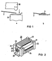
- 1 means a metallic base, for example a contact element, on which a paint-insulated wire 2 is to be contacted.
- Ultrasound welding can advantageously be used for this purpose, for which an ultrasound sonotrode with 10 and associated ultrasound anvil with 11 are indicated.
- the insulation layers are broken up by the mechanical effect and the metallic parts are contacted by friction welding with simultaneous deformation.
- a one-component adhesive is used as the adhesive. It is important for the intended use that the adhesive substance is thixotropic, i.e. dimensionally stable, is and hardens quickly. In automated production, a drop of the adhesive can then be applied to the welding point directly after welding, which hardens after passing through UV light after a few seconds, so that a shape 4 results which surrounds the deformed area of the wire 1.
- an RF choke is designated 20.
- Such chokes usually consist of a core 21, which can be made of ceramic, plastic or ferrite, with a single-layer or multi-layer winding 24 made of enamelled, insulated round wire.
- a core 21 which can be made of ceramic, plastic or ferrite, with a single-layer or multi-layer winding 24 made of enamelled, insulated round wire.
- the core 21 has end faces 22 with recesses 23, into which connection tabs 25 with a platelet surface are introduced on the front and rear sides.
- the connecting lugs 25 are bent at their free part so that they can be plugged onto printed circuit boards or the like.
- connection lug 25 must be contacted with the winding wire 24:
- the winding wire 24 is placed diagonally around the connection lug 25 and the end 26 of the winding wire 24 is welded on using ultrasound in the manner described above.
- a drop of the specified adhesive is then applied to the surface of the connecting lug 25.
- An approximately wart-shaped area 27 is formed, which covers the entire deformation area of the ultrasonic welding. After the adhesive has hardened, a mechanically stable connection is achieved.
- weld is also protected against climatic and corrosive influences.
Landscapes
- Engineering & Computer Science (AREA)
- Power Engineering (AREA)
- Manufacturing & Machinery (AREA)
- Manufacturing Cores, Coils, And Magnets (AREA)
- Manufacturing Of Electrical Connectors (AREA)
- Coils Or Transformers For Communication (AREA)
- Connections Effected By Soldering, Adhesion, Or Permanent Deformation (AREA)
Claims (1)
Applications Claiming Priority (2)
| Application Number | Priority Date | Filing Date | Title |
|---|---|---|---|
| DE19853513435 DE3513435A1 (de) | 1985-04-15 | 1985-04-15 | Verfahren zum abreisssicheren kontaktieren lackisolierter draehte, insbesondere zur anwendung bei elektronischen bauteilen |
| DE3513435 | 1985-04-15 |
Publications (3)
| Publication Number | Publication Date |
|---|---|
| EP0200014A1 EP0200014A1 (fr) | 1986-11-05 |
| EP0200014B1 EP0200014B1 (fr) | 1990-03-14 |
| EP0200014B2 true EP0200014B2 (fr) | 1994-08-24 |
Family
ID=6268048
Family Applications (1)
| Application Number | Title | Priority Date | Filing Date |
|---|---|---|---|
| EP86104429A Expired - Lifetime EP0200014B2 (fr) | 1985-04-15 | 1986-04-01 | Procédé de réalisation de contacts inarrachables pour des fils isolés par du vernis |
Country Status (3)
| Country | Link |
|---|---|
| EP (1) | EP0200014B2 (fr) |
| JP (1) | JPH0815126B2 (fr) |
| DE (2) | DE3513435A1 (fr) |
Families Citing this family (5)
| Publication number | Priority date | Publication date | Assignee | Title |
|---|---|---|---|---|
| DE3835818C3 (de) * | 1988-10-21 | 1996-02-08 | Stapla Ultraschalltechnik Gmbh | Verfahren und Vorrichtung zum Verbinden von Ankerwicklungsdrähten mit den Lamellen eines Hakenkollektors |
| DE4039527C1 (fr) * | 1990-12-11 | 1992-06-25 | Siemens Matsushita Components Gmbh & Co. Kg, 8000 Muenchen, De | |
| DE4313608A1 (de) * | 1993-04-26 | 1994-10-27 | Siemens Ag | Verfahren und Vorrichtung zum Kontaktieren von Wickelgütern an Anschlußelementen |
| DE4432740A1 (de) | 1994-09-14 | 1996-03-21 | Siemens Matsushita Components | Chip-Induktivität |
| JP3464444B2 (ja) * | 2000-10-30 | 2003-11-10 | 三菱電機株式会社 | 電磁機器 |
Family Cites Families (11)
| Publication number | Priority date | Publication date | Assignee | Title |
|---|---|---|---|---|
| US3271717A (en) * | 1961-06-05 | 1966-09-06 | Vincent C Gilbert | Electrical coil construction employing pressure sensitive adhesive |
| DE1903006A1 (de) * | 1969-01-22 | 1970-08-06 | Siemens Ag | Anschluss von Wickelspulen |
| US3590207A (en) * | 1969-06-16 | 1971-06-29 | Gen Electric | Method of joining wires of different diameters |
| JPS5287687A (en) * | 1976-01-16 | 1977-07-21 | Hitachi Ltd | Method for connecting enameled wire to terminal |
| DE2641508C2 (de) * | 1976-09-15 | 1978-09-21 | Siemens Ag, 1000 Berlin Und 8000 Muenchen | Vorrichtung zum Verbinden von unverdichteten, hochflexiblen, blanken oder isolierten Litzen aus Kupfer mit metallischen Trägern |
| DE2728914A1 (de) * | 1977-06-27 | 1979-01-04 | Hans Dipl Ing Rilling | Buchsenleiste fuer elektrische steckverbinder von flachbandkabeln |
| JPS5475061A (en) * | 1977-11-26 | 1979-06-15 | Citizen Watch Co Ltd | Structure of protective portion of coil terminal and its preparation |
| DE2757038A1 (de) * | 1977-12-21 | 1979-07-05 | Hans Dipl Ing Rilling | Buchsenleiste fuer elektrische steckverbinder von flachbandkabeln |
| JPS571213A (en) * | 1980-06-03 | 1982-01-06 | Omron Tateisi Electronics Co | Treating method for terminal of coil |
| NL188772C (nl) * | 1981-07-09 | 1992-09-16 | Tdk Corp | Inductantie. |
| JPS59198711A (ja) * | 1983-04-25 | 1984-11-10 | Tamura Seisakusho Co Ltd | コイルの端子固定方法 |
-
1985
- 1985-04-15 DE DE19853513435 patent/DE3513435A1/de not_active Withdrawn
-
1986
- 1986-04-01 DE DE8686104429T patent/DE3669624D1/de not_active Expired - Lifetime
- 1986-04-01 EP EP86104429A patent/EP0200014B2/fr not_active Expired - Lifetime
- 1986-04-11 JP JP61084028A patent/JPH0815126B2/ja not_active Expired - Fee Related
Also Published As
| Publication number | Publication date |
|---|---|
| DE3669624D1 (de) | 1990-04-19 |
| EP0200014A1 (fr) | 1986-11-05 |
| DE3513435A1 (de) | 1986-10-16 |
| JPH0815126B2 (ja) | 1996-02-14 |
| JPS61240617A (ja) | 1986-10-25 |
| EP0200014B1 (fr) | 1990-03-14 |
Similar Documents
| Publication | Publication Date | Title |
|---|---|---|
| DE69026188T2 (de) | Elektrischer Verbinder | |
| EP2130210B1 (fr) | Fusible thermique | |
| DE10139111B4 (de) | Verfahren für das Verbinden eines leitfähigen Klebers und einer Elektrode sowie einer verbundenen Struktur | |
| DE3329886C2 (de) | Verfahren zum Herstellen von Trocken-Elektrolyt-Kondensatoren | |
| DE2345149A1 (de) | Elektronisches hybrid-bauteil mit halbleiter-chips | |
| EP0301533A2 (fr) | Fusible électrique et méthode de sa fabrication | |
| DE1640471B2 (de) | Verfahren zum verbinden eines duennen drahtes mit einer anschlussklemme | |
| EP0200014B2 (fr) | Procédé de réalisation de contacts inarrachables pour des fils isolés par du vernis | |
| DE10009215C1 (de) | Steckverbinder sowie Verfahren zur Herstellung eines Steckverbinders | |
| DE19927947A1 (de) | Verfahren zum Herstellen eines Drahteinlageinduktors und durch dasselbe hergestellter Drahteinlageinduktor | |
| US4712723A (en) | Method for bonding an insulated wire element on a contact | |
| DE19645034C2 (de) | Ebene elektrische Schaltung und Verfahren zur Herstellung derselben | |
| WO1994014214A1 (fr) | Procede et dispositif pour enfoncer des elements metalliques dans des pieces de support | |
| DE3017364A1 (de) | Verfahren und vorrichtung zum verbinden eines leiters mit einem flachstecker | |
| DE19531970A1 (de) | Verfahren zur Herstellung einer Verbindung zwischen zumindest zwei elektrischen Leitern, von denen einer auf einem Trägersubstrat angeordnet ist | |
| DE3731969C2 (fr) | ||
| DE102006025661B4 (de) | Kontaktklemme zum Anschließen eines Litzenleiters an einen relativ dünnen Anschlussstift | |
| EP0702378B1 (fr) | Inductance de puce | |
| DE8600878U1 (de) | Elektrische Schaltungsplatte aus einem isolierenden Schichtstoff-Papiermaterial | |
| DE102005010350A1 (de) | LED-Herstellungsverfahren | |
| EP1236563B1 (fr) | Connexion électrique par soudage ultrasonique | |
| DE19618104A1 (de) | Verfahren zur Herstellung einer elektrisch leitenden Verbindung zwischen einem ummantelten Kupferdraht und einem elektrischen Leiter | |
| EP3631912A1 (fr) | Procédé de contact pour conducteurs isolés au vernis | |
| EP0651912A1 (fr) | Boitier miniaturise pour composants electroniques | |
| DE2031285A1 (de) | Verfahren 7um Herstellen einer An zahl plattchenformiger elektronischer Bauelemente mit Kunststoffgehäuse. Annr Matsuo Electric Co., Ltd , Osaka (Japan) |
Legal Events
| Date | Code | Title | Description |
|---|---|---|---|
| PUAI | Public reference made under article 153(3) epc to a published international application that has entered the european phase |
Free format text: ORIGINAL CODE: 0009012 |
|
| AK | Designated contracting states |
Kind code of ref document: A1 Designated state(s): DE FR GB IT SE |
|
| PUAB | Information related to the publication of an a document modified or deleted |
Free format text: ORIGINAL CODE: 0009199EPPU |
|
| PUAF | Information related to the publication of a search report (a3 document) modified or deleted |
Free format text: ORIGINAL CODE: 0009199SEPU |
|
| R17D | Deferred search report published (corrected) |
Effective date: 19861210 |
|
| RA1 | Application published (corrected) |
Date of ref document: 19861210 Kind code of ref document: A1 |
|
| 17P | Request for examination filed |
Effective date: 19870127 |
|
| 17Q | First examination report despatched |
Effective date: 19880822 |
|
| GRAA | (expected) grant |
Free format text: ORIGINAL CODE: 0009210 |
|
| AK | Designated contracting states |
Kind code of ref document: B1 Designated state(s): DE FR GB IT SE |
|
| GBT | Gb: translation of ep patent filed (gb section 77(6)(a)/1977) | ||
| REF | Corresponds to: |
Ref document number: 3669624 Country of ref document: DE Date of ref document: 19900419 |
|
| ET | Fr: translation filed | ||
| ITF | It: translation for a ep patent filed | ||
| PLBI | Opposition filed |
Free format text: ORIGINAL CODE: 0009260 |
|
| 26 | Opposition filed |
Opponent name: ROBERT BOSCH GMBH Effective date: 19901212 |
|
| ITTA | It: last paid annual fee | ||
| PGFP | Annual fee paid to national office [announced via postgrant information from national office to epo] |
Ref country code: FR Payment date: 19920428 Year of fee payment: 7 |
|
| PGFP | Annual fee paid to national office [announced via postgrant information from national office to epo] |
Ref country code: SE Payment date: 19920429 Year of fee payment: 7 |
|
| PGFP | Annual fee paid to national office [announced via postgrant information from national office to epo] |
Ref country code: GB Payment date: 19930319 Year of fee payment: 8 |
|
| PG25 | Lapsed in a contracting state [announced via postgrant information from national office to epo] |
Ref country code: SE Effective date: 19930402 |
|
| PG25 | Lapsed in a contracting state [announced via postgrant information from national office to epo] |
Ref country code: FR Effective date: 19931229 |
|
| REG | Reference to a national code |
Ref country code: FR Ref legal event code: ST |
|
| PG25 | Lapsed in a contracting state [announced via postgrant information from national office to epo] |
Ref country code: GB Effective date: 19940401 |
|
| PUAA | Information related to the publication of a b2 document modified |
Free format text: ORIGINAL CODE: 0009299PMAP |
|
| PUAH | Patent maintained in amended form |
Free format text: ORIGINAL CODE: 0009272 |
|
| STAA | Information on the status of an ep patent application or granted ep patent |
Free format text: STATUS: PATENT MAINTAINED AS AMENDED |
|
| 27A | Patent maintained in amended form |
Effective date: 19940824 |
|
| AK | Designated contracting states |
Kind code of ref document: B2 Designated state(s): SE |
|
| R27A | Patent maintained in amended form (corrected) |
Effective date: 19940824 |
|
| GBPC | Gb: european patent ceased through non-payment of renewal fee |
Effective date: 19940401 |
|
| EN3 | Fr: translation not filed ** decision concerning opposition | ||
| EUG | Se: european patent has lapsed |
Ref document number: 86104429.5 Effective date: 19931110 |
|
| APAC | Appeal dossier modified |
Free format text: ORIGINAL CODE: EPIDOS NOAPO |
|
| APAC | Appeal dossier modified |
Free format text: ORIGINAL CODE: EPIDOS NOAPO |
|
| PG25 | Lapsed in a contracting state [announced via postgrant information from national office to epo] |
Ref country code: IT Free format text: LAPSE BECAUSE OF NON-PAYMENT OF DUE FEES;WARNING: LAPSES OF ITALIAN PATENTS WITH EFFECTIVE DATE BEFORE 2007 MAY HAVE OCCURRED AT ANY TIME BEFORE 2007. THE CORRECT EFFECTIVE DATE MAY BE DIFFERENT FROM THE ONE RECORDED. Effective date: 20050401 |
|
| PGFP | Annual fee paid to national office [announced via postgrant information from national office to epo] |
Ref country code: DE Payment date: 20050531 Year of fee payment: 20 |
|
| APAH | Appeal reference modified |
Free format text: ORIGINAL CODE: EPIDOSCREFNO |