EP0193328A2 - Pulsgeneratoren zum Starten eines Lesevorganges - Google Patents
Pulsgeneratoren zum Starten eines Lesevorganges Download PDFInfo
- Publication number
- EP0193328A2 EP0193328A2 EP86301083A EP86301083A EP0193328A2 EP 0193328 A2 EP0193328 A2 EP 0193328A2 EP 86301083 A EP86301083 A EP 86301083A EP 86301083 A EP86301083 A EP 86301083A EP 0193328 A2 EP0193328 A2 EP 0193328A2
- Authority
- EP
- European Patent Office
- Prior art keywords
- signal
- phase
- read
- subcarrier
- synchronising
- Prior art date
- Legal status (The legal status is an assumption and is not a legal conclusion. Google has not performed a legal analysis and makes no representation as to the accuracy of the status listed.)
- Granted
Links
Images


Classifications
-
- H—ELECTRICITY
- H04—ELECTRIC COMMUNICATION TECHNIQUE
- H04N—PICTORIAL COMMUNICATION, e.g. TELEVISION
- H04N9/00—Details of colour television systems
- H04N9/44—Colour synchronisation
- H04N9/475—Colour synchronisation for mutually locking different synchronisation sources
-
- H—ELECTRICITY
- H04—ELECTRIC COMMUNICATION TECHNIQUE
- H04N—PICTORIAL COMMUNICATION, e.g. TELEVISION
- H04N9/00—Details of colour television systems
- H04N9/79—Processing of colour television signals in connection with recording
- H04N9/87—Regeneration of colour television signals
- H04N9/89—Time-base error compensation
- H04N9/896—Time-base error compensation using a digital memory with independent write-in and read-out clock generators
Definitions
- Read start pulse generators in accordance with the invention may, for example, be employed in image signal processing systems, for example in time base correctors of video tape recorders.
- An image signal processing system such as a video tape recorder, usually incorporates a time base corrector that causes a reproduced video signal to be written once in a memory, after analog to digital (A/D) conversion, and then read from the memory in synchronism with a stable reference pulse signal before digital to analog(D/A)conversion.
- the video signal is outputted together with a synchronising signal, a burst signal and a blank pulse signal all included in the reference pulse signal.
- the time base corrector includes a write clock generator and a read clock generator.
- the write clock generator generates a write start pulse signal to designate each head address of each. scanning line in the memory and a write clock signal to increment the address sequentially in writing the video signal; and the read clock generator generates a read start pulse signal to designate each head address of each scanning line in the memory and a read clock signal to increment the address sequentially in reading the video signal.
- an automatic phase controller usually is incorporated in each of the read clock generator and the write clock generator.
- a previously proposed read clock generator of a time base corrector is provided with various adjusting devices such as a horizontal synchronisation phase adjusting device, a colour subcarrier phase adjusting device, and a hue adjusting device, in addition to the horizontal synchronisation colour subcarrier phase adjusting device, if the foregoing adjusting devices are operated after the horizontal synchronisation colour subcarrier phase adjusting device has been operated, a problem arises in that the horizontal synchronisation colour subcarrier phase adjusting device needs to be adjusted again. That is, it is impossible to operate the other adjusting devices independently, thus giving rise to a complicated time base corrector adjusting operation.
- the invention also provides a read start pulse generator of an automatic subcarrier synchronising phase controller type for receiving a reference horizontal synchronising signal and a reference burst signal both separated from a reference pulse signal, the read start pulse generator comprising:
- Preferred embodiments of the present invention described hereinbelow provide read start pulse generators incorporated with a read clock generator of a time base corrector for a video tape recorder, for instance, in which it is unnecessary to readjust the automatic phase controller for colour subcarrier synchronisation even after the horizontal synchronisation phase, subcarrier phase, and/or hue have been adjusted.
- a previously proposed read start pulse generator will first be described in detail with respect to its application to a time base corrector (TBC) incorporated within an image signal processor, for instance a video tape recorder.
- TBC time base corrector
- Some image signal processors such as video tape recorders (VTRs), usually employ a time base corrector such as that shown in Figure 1 in which a reproduced video input signal VDIN is first converted into a corresponding digital signal by an analog to digital (A/D) converter 4 , stored in a memory or memory unit 6, read from the memory 6 in synchronism with a stable reference pulse signal VDREF and converted again into a corresponding analog signal by a digital to analog (D/A) converter 8 as video data.
- A/D analog to digital
- D/A digital to analog
- a reproduced synchronising signal SYNC is separated by a synchronisation separator 1 from the reproduced input signal VDIN, reproduced from a tape, and is applied to a write clock generator 2. Further, a reproduced burst signal BURST is separated from the reproduced input signal VDIN by a burst separator 3 and also is applied to the write clock generator 2.
- the write clock generator 2 generates a write clock signal WCK and a write start pulse signal WZERO in synchronism with the reproduced synchronisation signal SYNC and the reproduced burst signal BURST, both of which have time base fluctuations.
- the write clock signal WCK is applied to the A/D converter 4 as a sampling pulse signal and is applied also to a memory controller 5, together with the write start pulse signal WZERO.
- the memory controller 5 designates each head address of each scanning line in the memory 6 and thereafter writes image signal data for each scanning line (i.e. for each 1 H) in the memory 6 in sequence by sequentially incrementing the address in response to the write clock signal WCK.
- the data written in the memory 6 is read in response to a read clock signal RCK and a read start pulse signal RZERO generated by a read clock generator 7 in response to the reference pulse signal VDREF having a stable period. That is to say, the memory controller 5 designates each head address of the memory area at which data for each scanning line is stored in response to the read start pulse signal RZERO, and thereafter reads image signal data for each 1 H in sequence from the memory 6 by incrementing the address in response to the read clock signal RCK.
- the image signal data is converted into analog signals by the D/A converter 8, which is driven in response to the read clock signal RCK, and then is outputted to a phase adjuster 9.
- the phase adjuster 9 sends out a reproduced output signal VDOUT by adding a synchronising signal SYNCX, a burst signal BURSTX, and a blank pulse BLKX which are all included in the reference pulse signal VDREF within the read clock generator 7.
- the memory controller 5 automatically to adjust the timing (i.e. the phase) at which the head addresses are designated so that the head data of the image signal can repeatedly and reliably be written in or read from the memory area having predetermined head addresses whenever image signal data for each scanning line is written in or read from the memory 6.
- the memory controller 5 it is necessary to synchronise the timing, at which the write start pulse signal WZERO or the read start pulse signal RZERO is generated, with the colour subcarrier.
- the frequency of the colour subcarrier is 455/2 times the line frequency and, therefore, the phase of the subcarrier between two sequentially adjacent scanning lines is shifted by 1/2 of a cycle, it is necessary to shift the phases of the write start pulse signal WZERO sent from the write clock generator 2 and the read start pulse signal RZERO sent from the read crock generator 7 by 1/2 of a period (about 140 ns) of the colour subcarrier for each scanning line.
- the phase of the write start pulse signal WZERO and the phase of the read start pulse signal RZERO are both shifted by 1/2 of a period for each scanning line, the image signal data read from the memory 6 can perfectly be restored in phase relationship between writing and reading.
- an automatic phase controller (APC circuit) is provided in each of the write clock generator 2 and the read clock generator 7.
- VTRs for broadcasting stations use a read clock generator 7 as shown in Figure 2, in which, in order to effect matching with a device provided at a succeeding stage, the phases of the horizontal synchronising signal and the burst signal can be adjusted by any given phase difference value from the reference pulse signal VDREF (i.e. a reference signal of the station) where necessary.
- the read clock generator 7 of this type will now be described with reference to Figures 2 and 3.
- a horizontal synchronising signal forming circuit or generator 7A a horizontal synchronising signal HSYNCR included in the reference pulse signal VDREF is separated in a synchronisation separator 11 and then supplied to a phase comparator 12.
- a horizontal synchronisation frequency oscillator 13 of a voltage controlled oscillator (VCO) type supplies an oscillation output HCOSC, having a frequency nfH which is n times higher than the horizontal synchronisation frequency fH to a signal generator 14.
- the signal generator 14 In response to the oscillation output HCOSC, the signal generator 14 generates a horizontal synchronisation signal HSYNC which is supplied to the phase comparator 12 after the phase has been adjusted by a phase adjuster 15 made up of a phase shifter.
- the phase comparator 12 feeds back a phase error voltage PHE 1 representing the phase difference between the horizontal synchronisation signal HSYNC supplied from the phase adjuster 15 and the reference horizontal synchronisation signal HSYNCR to the horizontal synchronisation frequency oscillator 13 in order to control the oscillation frequency of the oscillator 13 so that the phase error voltage PHE1 becomes zero. Therefore, the horizontal synchronisation signal HSYNC provided by the signal generator 14 has a phase shift corresponding to a phase difference produced by the phase adjuster 15 relative to the phase of the reference horizontal synchronising signal HSYNCR.
- the phase adjuster 15 includes a horizontal synchronisation phase adjusting device 16.
- the phase-shift value of the adjusting device 16 can be adjusted freely by an operator operating the adjusting device 16 where necessary. As described above, it is possible freely to determine the phase difference between the horizontal synchronisation signal HSYNC and the reference horizontal synchronisation signal HSYNCR.
- the signal generator 14 outputs a synchronisation signal SYNCX and a blank signal BLKX (made up of a horizontal synchronising signal HD and a vertical synchronising signal VD) synchronised with the horizontal synchronisation signal HSYNC.
- the horizontal synchronising signal HSYNC is supplied to an automatic phase controller (APC) 7B for colour subcarrier synchronisation.
- the APC 7B receives the horizontal synchronising signal HSYNC directly at one switch input terminal P1 of a switch circuit 22 and receives it also at another switch input terminal P2 of the same switch circuit 22 after it has been delayed by 1/2 of a period (i.e. 140 ns) by a delay circuit 23.
- the switch circuit 22 operates to switch the switch input terminals P1 and P2 for each 1H section in response to a sequential line switching signal LAL, the logical level of which is inverted for each 1 H period on the basis of the reproduced horizontal synchronising signal HSYNC.
- the horizontal synchronising signal HSYNC is delayed by 1/2 of a period of the colour subcarrier for each 1 H section through the delay circuit 23 and then inputted as a trigger signal to a timer circuit 24 made up of two monostable multivibrators.
- the timer circuit 24 generates a timer output MODH indicative of time points near time points at which the read start pulse signal RZERO should be generated on the basis of the timing of the horizontal synchronising signal HSYNC.
- a pulse of the horizontal synchronising signal HSYNC ( Figure 3 (B2)) is received at a time point to through the switch input terminal P1 of the switch circuit 22 to cause the timer output MODH to rise to logic level "1" as shown in Figure 3 (D2).
- the timer circuit 24 operates in such a way that the timer output MODH falls to logic level "0" at a time point tt just prior to a time point t2 at which the read start pulse signal RZERO should be generated ( Figure 3 (E2)).
- the timer output MODH is supplied to a latch circuit 27.
- the latch circuit 27 operates in response to a read subcarrier signal RSC provided by a read signal generator or forming circuit 7D on the basis of an oscillator output BCOSC of a colour subcarrier frequency oscillator 26 in a colour subcarrier signal generator or forming circuit 7C.
- a timing corresponding to the time point t2 - ( Figure 3) at which the burst signal BURST ( Figure 3 (C2)) generated on the basis of the ocillation output BCOSC crosses zero in a positive-going sense the logic level of the timer output MODH is latched by the latch circuit 27.
- the read start pulse signal RZERO which is obtained at an output terminal of the latch circuit 27, falls from “1" to “0” at the time point t2 because the timer output MODH falls to "0" at the time point t 1 immediately before the time point t2, so that the reading of data from the memory 6 begins in response to this trailing edge.
- the timer circuit 24 receives the horizontal synchronisation signal HSYNC as a trigger signal through the delay circuit 23 and the switch input terminal P2 of the switch circuit 22. Therefore, as shown in Figure 3 (D1), the timer circuit 2 4 generates a timer output MODH which rises at a time point which is delayed by the delay time (140 ns) of the delay circuit 23 from the time point to. Thereafter, the timer output MODH falls to logic "0" at a time point t3 immediately before a time point t 4 at which the read start pulse signal RZERO should be generated.
- the phase of the burst signal BURST is delayed by 1/2 of a period of the colour burst signal (which corresponds to the delay time of the delay circuit 23) as compared with the case shown in Figure 3 (C2). Therefore, the time at which the timer output MODH of the timer circuit 2 4 falls occurs immediately before the read start pulse signal RZERO in the cases of both the (N)th and (N+1)th scanning line.
- the timer output MODH is compared with the read subcarrier signal RSC by a phase comparator 28.
- the read subcarrier signal RSC is formed by the read signal generator 7D on the basis of the burst signal BURST formed by the colour subcarrier signal generator 7C.
- a burst separator 31 separates the burst signal included in the reference pulse signal VDREF in response to a gate signal GATE supplied from the synchronisation separator 11, the resultant burst signal BURSTR being applied to a phase comparator 32.
- the colour subcarrier frequency oscillator 26 which is of a voltage controlled oscillator (VCO) type including a quartz oscillator, provides the oscillation output BCOSC which has a frequency 4fsc four times higher than the colour subcarrier frequency fsc, which output is divided by a 1/4 divider 33 and supplied to the phase comparator 32 as the burst signal BURST through a phase adjuster 34. Then, a phase error voltage PHE2 obtained by the phase comparator 32 is fed back to the colour subcarrier frequency oscillator 26 to cause it to provide an oscillation output BCOSC for allowing the phase error voltage PHE2 to become zero.
- VCO voltage controlled oscillator
- the phase adjuster 34 is made up of phase shifters and includes a subcarrier phase adjusting device 35.
- the phase difference between the burst signal BURSTX and the separated burst signal BURSTR can be adjusted freely on the basis of a phase difference value in the phase adjuster 34.
- the burst signal BURSTX is supplied to a phase adjuster 41, made up of phase shifters and included in the read signal generator 7D, in order to shift the phase thereof, and then the frequency thereof is multiplied by four in a 4/1 multiplier 42. Therefore, the read clock signal RCK, having a frequency 4fsc four times higher than the colour subcarrier frequency, is outputted from an output terminal of the 4/1 multiplier 42.
- the read clock signal RCK is supplied to a 1/4 divider 43, so that the read subcarrier signal RSC, having the frequency fsc of the colour subcarrier, can be obtained from an output terminal of the divider 43.
- An output of the phase adjuster 41 is applied to the 1/4 divider 43. as a reset signal to synchronise the operation of the divider with the burst signal, the phase of which is adjusted by the phase adjuster 41, so that the phase of the read subcarrier signal RSC is synchronised with the output of the phase adjuster 41.
- the phase adjuster 41 is supplied by an adder 45 with an addition output or sum of an adjustment output applied from a hue adjusting device 44 as a phase adjusting signal and a velocity error signal VER. Therefore, the phase differences between the read clock signal RCK and the burst signal BURSTX and between the read subcarrier signal RSC and the burst signal BURSTX can be adjusted on the basis of the adjustment output of the phase adjusting device 44 and the velocity error signal VER.
- the phase comparator 28 of the APC 7B for colour subcarrier synchronisation compares in phase the trailing edges of the timer output MODH ( Figure 3 (D2) and (D1 with the zero-crossing points of the burst signal BURST ( Figure 3 (C2) and (C1)), generates a phase error output PER indicative of the phase difference between the two, and applies the output PER to the timer circuit 24 as a timer time control signal.
- the timer circuit 24 operates in a state in which the phase error output PER indicates a small advance phase difference previously determined relative to the zero-crossing points of the burst signal BURST.
- the thus phase-controlled timer output MODH is applied as input data to the latch circuit 27 which is operative to latch at the zero-crossing points of the burst signal BURST and outputs a read start pulse signal RZERO falling to logic level "0" at the time points at which the burst signal BURST crosses zero. Therefore, the read start pulse signal RZERO can be generated securely, being synchronised with the zero-crossing points of the burst signal BURST, because the timer output MODH is allowed to fall to logic level "0" immediately before the time points (i.e. t2 and t4) at which video signal data should start to be read from the memory 6.
- the colour subcarrier synchronising APC 7B shown in Figure 2 is provided with a capacitor 51 and a switch circuit 52 at an output terminal of the phase comparator 28 in order to hold the phase error output PER and to supply a predetermined voltage level (e.g. ground voltage) through the switch circuit 52.
- the switch circuit 52 is on-off controlled by a detection output of an APC return level detector 54 through an OR gate 53.
- the capacitor 51 is grounded via the switch circuit 52 in order to return the phase error output PER to ground potential.
- phase error output PER of the phase comparator 28 changes to values at which pull-in operation is impossible
- the APC operation is returned to the normal operating state by the phase error output PER being locked forcibly to zero (volts) by the APC return level detector 54 and the switching circuit 52.
- the horizontal synchronising signal HSYNC is returned to the normal state
- the timer output MODH of the timer circuit 24 is returned to the nearest stable point (zero-crossing points of the burst signal)
- the timer circuit 24 is composed of a first monostable multivibrator 55 having a sufficiently long timer (delay) time and a second monostable multivibrator 56 having a sufficiently short timer (delay) time, for instance as short as about one period of the burst signal, and the phase error output PER of the phase comparator 28 is supplied to the first monostable multivibrator 55 through a buffer 57 as a timer time control signal.
- a horizontal synchronising colour subcarrier phase adjusting device 58 is provided for the second monostable multivibrator 56, so that the timing of the trailing edge of the timer output MODH can finely be adjusted by the adjusting device 58.
- the switching circuit 52 is arranged to be turned on by an adjustment mode signal ADJ via the OR gate 53.
- timer output MODH and the burst signal BURST are applied to a window detector 59 to light up a display element 60 when the phase difference lies within a predetermined window range.
- the window detector 59 detects that the phase of the timer output MODH is in close proximity to the stable points (i.e. any one of zero-crossing points) of the burst signal BURST.
- the colour subcarrier synchronising APC 7B is configured as described above, it is possible to adjust the phase of the trailing edge of the timer output MODH to be near the stable point by means of the phase comparator 28 and the APC return level detector 54 before the APC operation. That is, a timer time control signal of ground potential level is applied to the first monostable multivibrator 55 of the timer circuit 24 by applying an adjust mode signal ADJ to the switch circuit 52 through the OR gate 53 to turn on the switch circuit 52 and thus discharging the capacitor 51 for holding the phase error output of the phase comparator 28 to ground potential via the switch circuit 52. At this moment, the multivibrator 55 is controlled so as to have a timer or delay time of lock-in operation.
- the timer or delay time of the second monostable multivibrator 56 is adjusted by operating the phase synchronising colour subcarrier phase adjusting device 58 to light up the display element 60.
- the phase synchronising colour subcarrier phase adjusting device 58 to light up the display element 60.
- the adjust mode signal ADJ is switched to a normal operation state which is indicated by logic level "0" to switch the switch circuit 52, whereby the mode is switched to the APC operation based on the phase comparator 28 and the APC return-level detector 54.
- the timer output MODH has been adjusted to be near a stable point of the burst signal BURST, it is possible readily to pull in the timer output MODH to the stable point
- the previously proposed read clock generator shown in Figure 2 involves the following problems.
- the horizontal synchronising phase adjusting device 16 of the synchronising signal generator 7A is adjusted, or the subcarrier phase adjusting device 35 of the colour subcarrier signal generator 7C is adjusted, or the hue adjusting device 4 4 of the read signal generator 7D is adjusted, the adjustment condition that the display element 60 is illuminated by the output of the window detector 59 is destroyed, thus giving rise to a problem in that the timer circuit 24 needs to be adjusted again.
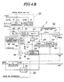
- FIG. 4 A description will now be given, with reference to Figure 4, of a first embodiment of the invention residing in a read start pulse generator included in a read clock generator.
- the read clock generator of Figure 4 is generally similar to that of Figure 2, as is shown by employing the same references for elements and sections corresponding to elements or sections of Figure 2. Consequently, the read clock generator of Figure 4 will be described only in so far as it differs from that of Figure 2.
- the configuration of the timer circuit 24 of the APC 7B for the colour subcarrier synchronisation is different from that shown in Figure 2. That is to say, in the read clock generator shown in Figure 4, the output of the switch circuit 22 is supplied to the monostable multivibrator 55 through a phase adjuster 65 made up of phase shifters, and outputs of the horizontal synchronising colour subcarrier phase adjusting device 58 and a phase adjust signal generator 66 are supplied through an adder 67 to the phase adjuster 65 as a phase adjust signal.
- An adjust signal CON1 provided by the horizontal synchronising phase adjusting device 16 of the synchronising signal generator 7A, an adjust signal CON2 obtained by the subcarrier phase adjusting device 35 of the colour subcarrier signal generator 7C, and an adjust signal CON3 obtained by the hue adjusting device 44 of the read signal generator 7D, are supplied to the phase adjust signal generator 66. Further, a phase control signal CONT is supplied to the phase adjuster 65 via the adder 67 in such a way as to have a value which prevents the signal supplied to the phase comparator 28 of the APC 7B for colour subcarrier synchronisation as a comparison input from being changed in phase when each adjusting device 16, 35 and 44 is operated to effect an adjustment
- a phase adjuster 70 is disposed between the signal generator 14 and phase adjuster 15 of the synchronising signal generator 7A.
- the phase adjuster 70 is composed of a phase shifter 71 for stepwise adjustment of the phase in time steps (i.e. 280 ns) of one period of the burst signal, a switching circuit 72 for manually switching output taps of the phase shifter, and a 1/4 divider 73 for dividing by four the output of the horizontal synchronising frequency oscillator 13 and for outputting a clock signal CK to the phase shifter 71, an output obtained at an output terminal of the switching circuit 72 being supplied to the phase adjuster 15.
- the phase adjuster 70 functions as an adjustment element for adjusting the phase difference between the horizontal synchronising signal HSYNC and the reference horizontal synchronising signal HSYNCR in cooperation with the horizontal synchronising phase adjusting device 16.
- a phase shift value of one i.e. 280 ns
- a coarse phase adjustment can be effected for each 280 ns by switching the output taps of the switching circuit 72 and, further, a fine adjustment of 280 ns or less can be effected by the horizontal synchronising signal adjusting device 16.
- the phase adjuster 15 can employ the circuit configuration shown in Figure 5. That is to say, a frequency input signal SO supplied from the phase adjuster 70 is received by a sawtooth wave generator 75 which outputs a sawtooth wave output S1 ( Figure 7(A)) having the period H of the horizontal synchronising signal.
- the sawtooth wave output S1 rises in level at a predetermined slope roughly during one period of the colour subcarrier frequency so as intermittently to generate a triangular portion during each period H.
- the sawtooth wave output S1 is compared with the adjust signal CON1 supplied from the horizontal synchronising phase adjusting device 16 by a comparator 76. During the 'time interval in which the sawtooth wave output S 1 is of higher level than the adjust signal CON1, an output signal S2 ( Figure 7(B)) outputted from an output terminal of the comparator 76 rises to logic level "1".
- the phase adjusters 34, 41, and 65 can employ the circuit configuration shown in Figure 6. in the same way as in the phase adjuster 15 (Figure 5), the phase adjusters 34, 41, and 65 receive a frequency input signal S10 which is applied to a sawtooth wave generator 77.
- a sawtooth wave output S11 ( Figure 8(A)) of the generator 77 is compared by a comparator 78 with the adjust signal CON2 supplied from the subcarrier phase adjusting device 35, the adjust signal CON3 supplied from the hue adjusting device 44, or an adjust signal CON4 supplied from the horizontal synchronising colour subcarrier phase adjusting device 58 in order to output a comparison output S12 ( Figure 8(B)).
- the comparison output S12 can be changed by controlling the phase of the leading edge at which it changes from logic level "0" to logic level "1" during the period Tsc according to the signal levels of the adjust signal CON2, CON3 or CON4.
- the read clock generator 7 can be adjusted in the same way as was described with reference to Figure 2. That is, the phase difference between the reference horizontal synchronising signal HSYNCR included in the reference pulse signal VDREF and the horizontal synchronising signal HSYNC is first adjusted by using the phase adjuster 70 and the phase adjusting device 16 both included in the synchronising signal generator 7A. At this time, a coarse adjustment can be effected in units of one or more periods - (i.e. 280 ns) of the burst signal by switching the coarse phase difference by switching the switching circuit 72 of the phase adjuster 70. In addition, a fine adjustment of less than one period can be effected by adjusting the phase adjusting device 16 of the phase adjuster 15.
- the phase difference between the burst signal included in the reference pulse signal VDREF and the burst signal of the TBC output is adjusted as occasion demands.
- phase difference bewteen the burst signal included in the reference pulse signal VDREF and the chrominance signal of the TBC output is adjusted.
- a range of adjustment of one period of the chrominance signal, that is within plus or minus 140 ns, is sufficient for the phase adjusting device 44.
- the switching circuit 52 of the colour subcarrier synchronising APC 7B is turned on in response to the adjustment mode signal ADJ, and the phase difference between the horizontal synchronising signal and the colour subcarrier is set by adjusting the phase adjusting device 58 when the phase error output PER of the phase comparator 28 is zero. This setting is continued until the display element 60 is lighted up. Thereafter, when the switching circuit 52 is turned off by switching the adjustment mode signal ADJ to the normal mode, it is possible to realise a state in which the timer output MODH of the timer circuit 24 follows the phase of the read subcarrier signal RSC whereby it is possible to send out a read start pulse signal RZERO of good reproducibility from the latch circuit 27 of the colour subcarrier synchronising APC 7B.
- the oscillation frequency of the horizontal synchronising frequency oscillator 13 can be controlled by the phase error output PHE1 of the phase comparator 12 in the synchronising signal generator 7A in accordance with the above adjustment operation, so that the phase of the horizontal synchronising signal SYNCX can be changed or controlled relative to the phase adjuster 9 ( Figure 1) of the time base corrector.
- the phase adjuster 65 since the adjust signal CON1 supplied from the phase adjusting device 16 to the phase adjuster 15 is supplied also to the phase adjust signal generator 66 so that the phase shift value of the phase adjuster 65 is changed or controlled, the phase adjuster 65 operates so as to compensate for the value corresponding to the change in phase of the horizontal synchronising signal HSYNC: as a result, the phase error output PER obtained at the output terminal of the phase comparator 28 is kept unchanged.
- the adjustment in the phase adjuster 70 is made in units of the burst signal period, only the adjustment value (i.e. within the phase difference of plus or minus 140 ns) on the basis of the adjustment signal CON1 supplied from the phase adjusting device 16 is generated by the phase comparator 28 as an effective value.
- phase shift value of the phase adjuster 65 can be changed.
- the phase of the timer output MODH supplied to the phase comparator 28 changes, the phase of the read subcarrier signal RSC supplied from the read signal generator 7D also changes according to the change of the burst signal BURSTX. Therefore, no change is produced in the phase error output PER of the phase comparator 28 due to the adjustment of the phase adjusting device 35, so that the APC 7B maintains the state in which the phase is locked.
- the hue adjusting device 44 of the read signal generator 7D when it is required to change the hue of the chrominance signal included in the output video signal VDOUT, it is sufficient to adjust the hue adjusting device 44 of the read signal generator 7D.
- the change produced in the adjust signal CON3 of the phase adjusting device 44 changes the phase shift value of the phase adjuster 41 through the adder 45, so that the phases of the read subcarrier signal RSC and the read clock signal RCK can be changed for control.
- the adjust signal CON3 of the phase adjusting device 44 changes or controls the phase shift value of the phase adjuster 65 through the phase adjust signal generator 66, it is possible to adjust the hue without producing a change in the phase error output PER of the phase comparator 28, so that the phase locked state can be maintained unchanged in the colour subcarrier synchronising APC 7B.
- Figure 9 shows a read clock generator in accordance with a second embodiment of the present invention.
- the read clock generator of Figure 4 is generally similar to that of Figure 2, as is shown by designating elements and sections corresponding to elements and sections shown in Figure 4 by the same reference numerals. Consequently, the read clock generator of Figure 9 will be described only in so far as it differs from that of Figure 4.
- the adjust signals CON1, CON2, and CON3 are not supplied to the phase adjuster 65 of the timer circuit 24.
- the system configuration is such that the phase adjustment is made at a rear stage of the APC loop. That is to say, in the colour subcarrier synchronising APC 7B of Figure 9, the frequency output S21 supplied from the phase adjuster 34 to the phase comparator 32 of the colour subcarrier signal generator 7C is supplied also to the phase comparator 28, the window detector 59 and the latch circuit 27, to all of which the timer output MODH is supplied.
- the frequency output S21 is in synchronism with the burst signal BURSTR separated from the reference pulse signal VDREF on the basis of the phase pull-in operation due to the phase comparator 32. Therefore, the colour subcarrier synchronising APC 7B operates so as to synchronise the horizontal synchronising signal HSYNC obtained by the synchronising signal generator 7A with the burst signal of the reference pulse signal VDREF.
- the system configuration is such that the phase adjuster 70 (including the phase shifter 71, the switching circuit 72 and the divider 73) is disposed between the signal generator 1 4 and the phase adjuster 15.
- the switching circuit 72 is switched, it is possible coarsely to adjust the phases of the horizontal synchronising signal SYNCX the blank signal BLKX (HD and VD signals) and a field signal FIELD all obtained from the signal generator 14 by switching the switching circuit 72.
- fine phase adjustment within one period of the burst signal (that is, within plus or minus 140 ns) can be made by the horizontal synchronising phase adjusting device 16.
- the horizontal synchronising signal HSYNC sent to the colour subcarrier synchronising APC 7B can be taken from the input terminal of the phase comparator 12 on the oscillation frequency signal side. Therefore, if the adjusting device 16 is adjusted, the phase of the horizontal synchronising signal HSYNC does not change. Therefore, the point at which the phase of the horizontal synchronising signal HSYNC is synchronised with the reference horizontal synchronising signal HSYNCR is different from that shown in Figure 4 .
- the output 270 of the latch circuit 27 of the colour subcarrier synchronising APC 7B is not used directly as the read start pulse signal RZERO, but instead is supplied to a phase shifter 82 provided in a phase adjuster 81 and driven by the frequency output S21.
- the phase shifter 82 has a plurality of phase outputs having' different phase shift values within one period of the burst signal. These phase outputs are selected by a switching circuit 83, the operation of which is linked with that of the switching circuit 72, and then supplied to a phase shifter 84.
- phase shifter 84 the phase shift value (within plus or minus 140 ns) within one period of the burst signal is controlled by a control signal supplied from a phase adjust signal generator 85.
- the adjust signal CON2 of the subcarrier phase adjusting device 35 and the adjust signal CON3 of the hue adjusting device 44 are supplied to the phase adjust signal generator 85.
- a control signal corresponding to this phase shift value is supplied to the phase shifter 84 in order to shift the phase of the output 270 of the latch circuit 27.
- the output 270 is supplied to an output latch circuit 90.
- the read subcarrier signal RSC is supplied as a drive signal to the output latch circuit 90. in this way, a read start pulse signal RZERO synchronised with the read subcarrier signal RSC is outputted from the output latch-circuit 90.
- the colour subcarrier synchronising APC 7B synchronises the horizontal synchronising signal HSYNC, the frequency signal of which is in synchronism with the horizontal synchronising signal HSYNCR separated from the reference pulse signal VDREF, with the frequency output S21 synchronised with the burst signal BURSTR separated from the reference pulse signal VDREF on the basis of the APC loop in the comparator 28. Further, the APC 7B latches the phase which is the reference of the read start pulse by means of the latch circuit 27.
- the latch output 270 is shifted by the phase adjuster 81 by a phase shift value corresponding to that mentioned above. Therefore, the phase of the latch output 270 is adjusted by the value corresponding to the phase differences produced in the read subcarrier signal RSC and the read clock signal RCK due to the phase adjusting devices 35 and 44, and is latched by the latch circuit 90 in synchronism with the read subcarrier signal RSC.
- the phase of the read start pulse signal RZERO is maintained while maintaining the phase pull-in status obtained in the colour subcarrier synchronising APC 7B.
- phase adjusting devices when the phases of the read horizontal synchronising signal HSYNC and the read subcarrier signal RSC are adjusted by the phase adjusting devices, it is possible to obtain a predetermined phase with sufficient reproduction, whereby it is possible to obtain a good reproducible output image signal VD from the memory.
- the embodiments of the present invention described above provide that, after the phases of the horizontal synchronising signal and the burst signal have been adjusted to the optimum phase in the colour subcarrier synchronising APC 7B, even if the phase of the horizontal synchronising signal, the burst signal or the chrominance signal of the output video signal is adjusted by any given phase shift value relative to the phase of the horizontal synchronising signal, the burst signal or the chrominance signal of the reference pulse signal VDREF, it is nonetheless possible to obtain a read start pulse generator by which it is possible securely to maintain the optimum phase synchronisation relationships between the horizontal synchronising signal and the burst signal without any need for any other complicated operations.
Landscapes
- Engineering & Computer Science (AREA)
- Multimedia (AREA)
- Signal Processing (AREA)
- Processing Of Color Television Signals (AREA)
- Television Signal Processing For Recording (AREA)
- Credit Cards Or The Like (AREA)
- Electrophonic Musical Instruments (AREA)
- Control Of Stepping Motors (AREA)
Priority Applications (1)
| Application Number | Priority Date | Filing Date | Title |
|---|---|---|---|
| AT86301083T ATE64055T1 (de) | 1985-02-16 | 1986-02-17 | Pulsgeneratoren zum starten eines lesevorganges. |
Applications Claiming Priority (2)
| Application Number | Priority Date | Filing Date | Title |
|---|---|---|---|
| JP60028913A JPS61189094A (ja) | 1985-02-16 | 1985-02-16 | 読出スタ−トパルス発生回路 |
| JP28913/85 | 1985-02-16 |
Publications (3)
| Publication Number | Publication Date |
|---|---|
| EP0193328A2 true EP0193328A2 (de) | 1986-09-03 |
| EP0193328A3 EP0193328A3 (en) | 1988-06-29 |
| EP0193328B1 EP0193328B1 (de) | 1991-05-29 |
Family
ID=12261637
Family Applications (1)
| Application Number | Title | Priority Date | Filing Date |
|---|---|---|---|
| EP86301083A Expired - Lifetime EP0193328B1 (de) | 1985-02-16 | 1986-02-17 | Pulsgeneratoren zum Starten eines Lesevorganges |
Country Status (8)
| Country | Link |
|---|---|
| US (1) | US4714954A (de) |
| EP (1) | EP0193328B1 (de) |
| JP (1) | JPS61189094A (de) |
| KR (1) | KR940006592B1 (de) |
| AT (1) | ATE64055T1 (de) |
| AU (1) | AU578517B2 (de) |
| CA (1) | CA1270943A (de) |
| DE (1) | DE3679420D1 (de) |
Cited By (2)
| Publication number | Priority date | Publication date | Assignee | Title |
|---|---|---|---|---|
| GB2252691A (en) * | 1990-10-19 | 1992-08-12 | Rca Licensing Corp | Signal time scaling apparatus |
| DE102007042833A1 (de) | 2007-09-10 | 2009-03-12 | Walter Ag | Strahlbehandelter Schneideinsatz und Verfahren |
Families Citing this family (12)
| Publication number | Priority date | Publication date | Assignee | Title |
|---|---|---|---|---|
| JP2655650B2 (ja) * | 1987-08-18 | 1997-09-24 | 三菱電機株式会社 | 時間軸補正装置 |
| JP2737346B2 (ja) * | 1990-02-19 | 1998-04-08 | ソニー株式会社 | 映像信号の時間差補正装置 |
| US5258780A (en) * | 1990-05-09 | 1993-11-02 | Ricoh Company, Ltd. | Beam recorder forming low density dots |
| JP2718311B2 (ja) * | 1991-12-27 | 1998-02-25 | 日本ビクター株式会社 | 時間軸補正装置 |
| JP3183967B2 (ja) * | 1992-10-16 | 2001-07-09 | パイオニアビデオ株式会社 | ディジタルタイムベースコレクタ |
| US5844621A (en) * | 1995-06-21 | 1998-12-01 | Sony Corporation | Burst gate pulse generator |
| US6043850A (en) * | 1997-05-08 | 2000-03-28 | Sony Corporation | Burst gate pulse generator circuit |
| US6380980B1 (en) * | 1997-08-25 | 2002-04-30 | Intel Corporation | Method and apparatus for recovering video color subcarrier signal |
| US5995164A (en) * | 1997-09-29 | 1999-11-30 | Zilog, Incorporated | Reduction of color transition distortions in NTSC/PAL encoder |
| US7139037B1 (en) * | 1997-09-29 | 2006-11-21 | Zilog, Inc. | Circle correction in digital low-pass filter |
| US6163346A (en) * | 1997-09-29 | 2000-12-19 | Zilog, Incorporated | Dot crawl reduction in NTSC/PAL graphic encoder |
| DE102004047831B4 (de) * | 2004-09-29 | 2007-05-10 | Micronas Gmbh | Verfahren bzw. Schaltung zum Bereitstellen eines Farbträgers |
Family Cites Families (11)
| Publication number | Priority date | Publication date | Assignee | Title |
|---|---|---|---|---|
| JPS5838011B2 (ja) * | 1976-07-05 | 1983-08-19 | ソニー株式会社 | 発振回路 |
| JPS53148317A (en) * | 1977-05-31 | 1978-12-23 | Sony Corp | Error correction unit for time axis |
| JPS54138333A (en) * | 1978-04-20 | 1979-10-26 | Sony Corp | Processing circuit for carrier chrominance signal |
| JPS56166686A (en) * | 1980-05-28 | 1981-12-21 | Pioneer Video Corp | Timing axis variation elimination device of video disk reproducer |
| JPS5713880A (en) * | 1980-06-26 | 1982-01-23 | Sony Corp | Line id detecting circuit |
| JPS5715586A (en) * | 1980-07-02 | 1982-01-26 | Sony Corp | Code modulator for video signal |
| DE3026473A1 (de) * | 1980-07-12 | 1982-02-04 | Robert Bosch Gmbh, 7000 Stuttgart | Verfahren zum ausgleich von zeitfehlern |
| US4562457A (en) * | 1982-12-23 | 1985-12-31 | Grumman Aerospace Corporation | Sync generator, video processor |
| JPS60172479U (ja) * | 1984-04-21 | 1985-11-15 | パイオニア株式会社 | Pal方式カラ−信号処理装置 |
| JPS6133575U (ja) * | 1984-07-28 | 1986-02-28 | ソニー株式会社 | クロツク形成回路 |
| JPH0669230B2 (ja) * | 1984-10-22 | 1994-08-31 | ソニー株式会社 | 再生映像信号の処理用信号発生装置 |
-
1985
- 1985-02-16 JP JP60028913A patent/JPS61189094A/ja active Pending
-
1986
- 1986-01-30 KR KR1019860000621A patent/KR940006592B1/ko not_active Expired - Fee Related
- 1986-02-05 US US06/826,223 patent/US4714954A/en not_active Expired - Fee Related
- 1986-02-07 CA CA000501349A patent/CA1270943A/en not_active Expired - Lifetime
- 1986-02-14 AU AU53486/86A patent/AU578517B2/en not_active Ceased
- 1986-02-17 EP EP86301083A patent/EP0193328B1/de not_active Expired - Lifetime
- 1986-02-17 DE DE8686301083T patent/DE3679420D1/de not_active Expired - Lifetime
- 1986-02-17 AT AT86301083T patent/ATE64055T1/de not_active IP Right Cessation
Cited By (3)
| Publication number | Priority date | Publication date | Assignee | Title |
|---|---|---|---|---|
| GB2252691A (en) * | 1990-10-19 | 1992-08-12 | Rca Licensing Corp | Signal time scaling apparatus |
| GB2252691B (en) * | 1990-10-19 | 1995-03-08 | Rca Licensing Corp | Signal time scaling apparatus |
| DE102007042833A1 (de) | 2007-09-10 | 2009-03-12 | Walter Ag | Strahlbehandelter Schneideinsatz und Verfahren |
Also Published As
| Publication number | Publication date |
|---|---|
| US4714954A (en) | 1987-12-22 |
| AU5348686A (en) | 1986-08-21 |
| EP0193328A3 (en) | 1988-06-29 |
| ATE64055T1 (de) | 1991-06-15 |
| EP0193328B1 (de) | 1991-05-29 |
| AU578517B2 (en) | 1988-10-27 |
| JPS61189094A (ja) | 1986-08-22 |
| KR940006592B1 (ko) | 1994-07-22 |
| DE3679420D1 (de) | 1991-07-04 |
| KR860006780A (ko) | 1986-09-15 |
| CA1270943A (en) | 1990-06-26 |
Similar Documents
| Publication | Publication Date | Title |
|---|---|---|
| EP0193328B1 (de) | Pulsgeneratoren zum Starten eines Lesevorganges | |
| US4438456A (en) | Time base corrector | |
| US4249198A (en) | Phase locking system for television signals | |
| EP0179590B1 (de) | Phasenreglerschaltungen für Zeitbasiskorrekturglieder | |
| JPS5923517B2 (ja) | テレビジヨン信号同期装置 | |
| US4689676A (en) | Television video signal synchronizing apparatus | |
| US4038683A (en) | Television synchronizing generator | |
| US4914509A (en) | Color video signal synthesizer | |
| EP0421486B1 (de) | Skewfehlerkorrekturschaltung für Videosignalwiedergabegerät | |
| US4714965A (en) | Write clock pulse generator used for a time base corrector | |
| US5760839A (en) | Horizontal synchronizing apparatus | |
| US4677459A (en) | Reference signal generator | |
| US5031031A (en) | Video signal processing apparatus | |
| JP3056555B2 (ja) | 時間軸誤差補正用基準信号記録及び再生回路 | |
| GB1468465A (en) | Timing correction for electrical pulse signals | |
| JP2687484B2 (ja) | 自動周波数制御回路 | |
| JPS58114587A (ja) | バ−ストロツク基準信号発生回路 | |
| JPH01119183A (ja) | テレビジョン信号の時間軸圧縮装置 | |
| JPH06237468A (ja) | 外部同期回路 | |
| JPH01132284A (ja) | 画像メモリ制御装置 | |
| JPS5940352B2 (ja) | カラ−テレビジョン信号処理装置 | |
| JPS61184991A (ja) | バ−スト同期連続波信号発生回路 | |
| JPH0779413A (ja) | タイムベースコレクタ回路 | |
| JPH09107527A (ja) | クロック生成回路 | |
| JPH02249389A (ja) | Fm変調回路 |
Legal Events
| Date | Code | Title | Description |
|---|---|---|---|
| PUAI | Public reference made under article 153(3) epc to a published international application that has entered the european phase |
Free format text: ORIGINAL CODE: 0009012 |
|
| AK | Designated contracting states |
Kind code of ref document: A2 Designated state(s): AT DE FR GB NL |
|
| PUAL | Search report despatched |
Free format text: ORIGINAL CODE: 0009013 |
|
| AK | Designated contracting states |
Kind code of ref document: A3 Designated state(s): AT DE FR GB NL |
|
| 17P | Request for examination filed |
Effective date: 19881123 |
|
| 17Q | First examination report despatched |
Effective date: 19900720 |
|
| GRAA | (expected) grant |
Free format text: ORIGINAL CODE: 0009210 |
|
| AK | Designated contracting states |
Kind code of ref document: B1 Designated state(s): AT DE FR GB NL |
|
| REF | Corresponds to: |
Ref document number: 64055 Country of ref document: AT Date of ref document: 19910615 Kind code of ref document: T |
|
| REF | Corresponds to: |
Ref document number: 3679420 Country of ref document: DE Date of ref document: 19910704 |
|
| ET | Fr: translation filed | ||
| PLBE | No opposition filed within time limit |
Free format text: ORIGINAL CODE: 0009261 |
|
| STAA | Information on the status of an ep patent application or granted ep patent |
Free format text: STATUS: NO OPPOSITION FILED WITHIN TIME LIMIT |
|
| 26N | No opposition filed | ||
| PGFP | Annual fee paid to national office [announced via postgrant information from national office to epo] |
Ref country code: GB Payment date: 19970210 Year of fee payment: 12 |
|
| PGFP | Annual fee paid to national office [announced via postgrant information from national office to epo] |
Ref country code: FR Payment date: 19970211 Year of fee payment: 12 |
|
| PGFP | Annual fee paid to national office [announced via postgrant information from national office to epo] |
Ref country code: DE Payment date: 19970221 Year of fee payment: 12 |
|
| PGFP | Annual fee paid to national office [announced via postgrant information from national office to epo] |
Ref country code: AT Payment date: 19970225 Year of fee payment: 12 |
|
| PGFP | Annual fee paid to national office [announced via postgrant information from national office to epo] |
Ref country code: NL Payment date: 19970227 Year of fee payment: 12 |
|
| PG25 | Lapsed in a contracting state [announced via postgrant information from national office to epo] |
Ref country code: GB Free format text: LAPSE BECAUSE OF NON-PAYMENT OF DUE FEES Effective date: 19980217 Ref country code: AT Free format text: LAPSE BECAUSE OF NON-PAYMENT OF DUE FEES Effective date: 19980217 |
|
| PG25 | Lapsed in a contracting state [announced via postgrant information from national office to epo] |
Ref country code: FR Free format text: THE PATENT HAS BEEN ANNULLED BY A DECISION OF A NATIONAL AUTHORITY Effective date: 19980228 |
|
| PG25 | Lapsed in a contracting state [announced via postgrant information from national office to epo] |
Ref country code: NL Free format text: LAPSE BECAUSE OF NON-PAYMENT OF DUE FEES Effective date: 19980901 |
|
| GBPC | Gb: european patent ceased through non-payment of renewal fee |
Effective date: 19980217 |
|
| NLV4 | Nl: lapsed or anulled due to non-payment of the annual fee |
Effective date: 19980901 |
|
| PG25 | Lapsed in a contracting state [announced via postgrant information from national office to epo] |
Ref country code: DE Free format text: LAPSE BECAUSE OF NON-PAYMENT OF DUE FEES Effective date: 19981103 |
|
| REG | Reference to a national code |
Ref country code: FR Ref legal event code: ST |