EP0146357B1 - Dispositif de mémoire à semi-conducteur - Google Patents
Dispositif de mémoire à semi-conducteur Download PDFInfo
- Publication number
- EP0146357B1 EP0146357B1 EP84308728A EP84308728A EP0146357B1 EP 0146357 B1 EP0146357 B1 EP 0146357B1 EP 84308728 A EP84308728 A EP 84308728A EP 84308728 A EP84308728 A EP 84308728A EP 0146357 B1 EP0146357 B1 EP 0146357B1
- Authority
- EP
- European Patent Office
- Prior art keywords
- cell
- redundant
- group
- block
- cells
- Prior art date
- Legal status (The legal status is an assumption and is not a legal conclusion. Google has not performed a legal analysis and makes no representation as to the accuracy of the status listed.)
- Expired - Lifetime
Links
Images


Classifications
-
- G—PHYSICS
- G11—INFORMATION STORAGE
- G11C—STATIC STORES
- G11C11/00—Digital stores characterised by the use of particular electric or magnetic storage elements; Storage elements therefor
- G11C11/21—Digital stores characterised by the use of particular electric or magnetic storage elements; Storage elements therefor using electric elements
- G11C11/34—Digital stores characterised by the use of particular electric or magnetic storage elements; Storage elements therefor using electric elements using semiconductor devices
- G11C11/40—Digital stores characterised by the use of particular electric or magnetic storage elements; Storage elements therefor using electric elements using semiconductor devices using transistors
-
- G—PHYSICS
- G11—INFORMATION STORAGE
- G11C—STATIC STORES
- G11C29/00—Checking stores for correct operation ; Subsequent repair; Testing stores during standby or offline operation
- G11C29/70—Masking faults in memories by using spares or by reconfiguring
- G11C29/78—Masking faults in memories by using spares or by reconfiguring using programmable devices
- G11C29/80—Masking faults in memories by using spares or by reconfiguring using programmable devices with improved layout
- G11C29/808—Masking faults in memories by using spares or by reconfiguring using programmable devices with improved layout using a flexible replacement scheme
-
- G—PHYSICS
- G11—INFORMATION STORAGE
- G11C—STATIC STORES
- G11C29/00—Checking stores for correct operation ; Subsequent repair; Testing stores during standby or offline operation
- G11C29/70—Masking faults in memories by using spares or by reconfiguring
- G11C29/78—Masking faults in memories by using spares or by reconfiguring using programmable devices
- G11C29/84—Masking faults in memories by using spares or by reconfiguring using programmable devices with improved access time or stability
- G11C29/846—Masking faults in memories by using spares or by reconfiguring using programmable devices with improved access time or stability by choosing redundant lines at an output stage
Definitions
- the present invention relates to a semiconductor memory device, in particular, it relates to a semiconductor memory device providing redundant cells.
- the provision of a large number of redundant cell groups is useful if a large number of defective memory cells are produced in a cell block.
- the provision of so many redundant cell groups is unnecessary, in that there is no use for them.
- usually, only one column or 2 to 3 columns of redundant cell groups are provided (per cell block).
- the redundant cell groups are linked exclusively to individual cell blocks.
- a redundant cell group When a redundant cell group is linked to an individual cell block, the following problems arise. That is, suppose that one column of redundant cells is provided for each cell block, and that two defective memory cells existing in different columns are produced in a first cell block but no defective cells are produced in a second cell block. In this case, although there are two redundant cell groups and two defective memory cells, the two redundant cell groups are linked to different cell blocks, and therefore, the redundant cell group in the second cell block cannot be used for the first cell block. Thus, only one redundant cell group can be utilised, to replace only one of the defective cells of the first cell block; the other defective cell cannot be replaced and the functioning of the memory device is deteriorated.
- PCT/US82/01826 discloses such a semiconductor memory device, in which spare columns of cells can be assigned to replace defective columns in any of eight bit segments.
- special column address switches are provided to activate each spare column in response to a column address of a defective column, and the outputs of the column address switches are multiplexed together with the output of normal columns of cells.
- US-A-4,346,459 discloses another such semiconductor memory device, which has special spare column select circuits which are switched during normal operation of the device, and hence has similar drawbacks.
- a semiconductor memory device comprising: first and second cell blocks, each comprising a plurality of cell groups, each cell group comprising a plurality of memory cells; a redundant cell group comprising a plurality of memory cells; first and second data buses corresponding respectively to the first and second cell blocks; decoder circuitry for selecting one of the cell groups; and switching circuitry responsive to said decoder circuitry for connecting the redundant cell group to either of said first or second data buses corresponding to the first and second cell blocks; characterised in that the redundant cell group is arranged between the first and second cell blocks; each cell group is connected to the data bus corresponding to its block via a respective selection gate controlled by said decoder circuitry; and in that the switching circuitry comprises gates arranged, and controlled by said decoder circuitry, in parallel with said selection gates, and permanently-settable switch circuits for permanently connecting the redundant cell group to either of said first or second data buses.
- Figure 1 shows one example of a conventional semiconductor memory device providing redundant cells.
- 10 and 12 represent cell blocks and 14 and 16 redundant cell groups.
- the cell blocks 10 and 12 arrange the memory cells at cross points of many word lines and bit lines (or row lines and column lines), and Y o to Y n are signals for selecting the bit lines.
- the word lines (not shown in the drawing), extend in a horizontal direction, and redundant cells are provided for one bit line (1 column) and are selected by a selection signal Y a .
- Numerals 18 and 20 are data buses and 22 and 24 are I/O (input output) buffers.
- This memory is organized for 2 bit output, so that when memory cells are selected by any address, the corresponding memory cells in cell blocks 10 and 12 are read out, and one bit from each I/O buffer 22 and 24, i.e., a total of two bits, are output at the same time.
- MC is a memory cell
- SRAM static random access memory
- RD is a row decoder, which receives word line selection addresses A o ⁇ A n and selects a word line WL when these addresses are at a low (L) level.
- the word lines WL extend over the cell block 10, the redundant cell groups 14, 16, and the cell block 12, and each word line WL is selected at the same time by the word line address.
- the I/O buffers include a sense amplifier SA and an input (write) data buffer O/N, etc.
- ROM read-only memory
- a column decoder which outputs Y o ⁇ Y n is made noneffective (all outputs of the decoder are made at a low level), and a signal Y a for selecting a redundant cell group is generated.
- the word lines are common to the cell blocks and redundant cell groups, so that the memory cells on the word lines for the redundant memory cell groups are selected instead of the defective memory cells.
- the provision of a large number of redundant cell groups is useful if a large number of defective memory cells are produced in the cell block.
- the provision of so many redundant cell groups is unnecessary, in that there is no use for them.
- the redundant cell groups are linked exclusively to an individual cell block. That is, as shown in Fig. 1, the redundant cell group 14 is linked to cell block 10 and the redundant cell group 16 is linked to cell block 12. This is determined by to which data bus the redundant cell group is connected.
- a redundant cell group When a redundant cell group is linked to a cell block in such a manner, the following problems arise. That is, suppose that one column of the redundant cells is provided for each cell block, and that two defective memory cells linked to different columns are produced in cell block 10 but no defective cells are produced in cell block 12. In this case, although there are two redundant cell groups and two defective memory cells, the two redundant cell groups are linked to different cell blocks, and therefore, the redundant cell group 16 cannot be used for cell block 10. Thus, only one redundant cell group 14 can be used to replace one defective cell , and therefore, the other defective memory cell cannot be replaced and the functioning of the memory device is impaired.
- FIG. 3 shows an embodiment of the present invention in which the same elements as in Fig. 1 are designated by the same symbols.
- switches S1 ⁇ S3 are provided to connect the redundant cell groups 14 and 16 to either of the data buses 18 and 20. Immediately after the memory device is manufactured, the switches S1 ⁇ S3 are open. When no defective memory cell are found in the cell block 10, the redundant cell group 14 is not used, and when the defective memory cell exists in a column in the cell block 10, the switch S2 is closed and the defective memory cell can be replaced by the redundant cell group 14. The same applies to the cell block 12. Up to this point, the device is similar to the conventional system.
- the switches S1 ⁇ S3 are initially open, and are closed only when necessary, the switches may be comprised of a poly-crystalline silicon fuse. When a switch is to be closed, the fuse is melted by supplying a current or by a laser beam.
- the switches S1 ⁇ S3 are initially open and are closed only when necessary, therefore the structure as shown in Figs. 4A and 4C may be used.
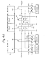
- FIG. 4A shows details of the switching circuit shown in Fig. 3.
- gate transistors 41a, 42a, 43a; 41b, 42b, 43b; ... 41n, 42n, 43n are connected to Y decoders i, j, ... k, respectively, and gate transistors 44, 45 and 46 are connected between I/O inputs (data buses) (1) and (2).
- One terminal of each transistor 42a and 42b is connected to the transistor 47
- one terminal of each transistor 43a and 43b is connected via transistors 48 and 49 to the transistor 42n
- the transistor 41n is connected to the transistor 50.
- the transistors 44 and 47 are controlled by an input from a fuse terminal F a
- the transistors 46 and 49 are controlled by an input from a fuse terminal F b
- the transistors 45 and 50 are controlled by an input from a fuse terminal F c .
- Figure 4B shows the construction of the fuse (ROM) in each Y decoder wherein, in Fig. 4B, 51a and 52a represent a high resistance,53a and 54a represent fuses, and 50a represents a gate circuit which receives the outputs of the fuse shown in (b) and (c) of Fig. 4B.
- Figure 4C shows the construction of the fuses (Fa, Fb, Fc) which correspond to the sequences (groups) of the redundant cells.
- 55 ⁇ 57 represent high resistances
- 58 ⁇ 60 represent fuses.
- fuses are made of material such as poly-crystalline silicon, and the transistors are field effect transistors (FETs).
- FETs field effect transistors
- the gate of the transistor is connected via the fuse F to ground, so that it is in an OFF state.
- the transistor is pulled up via the high resistances such as 51a, ..., 55, etc. to the electric source V c , so that it becomes in an ON state.
- the fuse F is not melted, the current flows from the electric source V c via the high resistance and the fuse to ground.
- the high resistance is used as the resistor R, this current can be decreased to a small value such as of the order of a pico ampere.
- Figure 5 is another embodiment corresponding to Fig. 4B.
- Fig. 4B if one fuse such as 53a is melted, the signal F i becomes "L” automatically, so that the transistor 41a is OFF.
- the structure is such that if at least one fuse corresponding to fuse 53a or 54a is melted, the fuse corresponding to 61a also melts, so that the signal F i becomes "L” and the transistor 41a is OFF.
- Figure 6 is a flowchart showing the operation of the device shown in Figs. 4A ⁇ 4C.
- block 71 if a failure is detected, block 71 is transferred to block 72.
- block 72 if one column in block 1 is detected, the fuse corresponding to the failed column i and the fuse F a are melted in block 73, so that the entire device is tested (block 74).
- block 72 if more than one failed column occurs in block 1, block 72 is transferred to block 75 and the failed columns are examined.
- the memory device may have a one bit organization by which one memory cell is selected by one address,or a plurality bit organization by which a plurality of cells are selected at the same time by one address.
- Figures 1 and 3 show a memory having a two bit construction, and a multibit organization such as 8 bits may exist in a 64 KRAM.
- the number of cell blocks and I/O buffers provided corresponds to the number of bits.
- 10A, 12A, ..., 12D are cell blocks and 22A, 24A, ..., 24D are I/O buffers.
- four circuits as shown in Fig. 2 may be provided, so that a 64 KRAM having an 8 K x 8 bits organization can be obtained.
- the redundant cell groups 14A and 16A are redundant cell groups corresponding to each cell block.
- the redundant cell groups 14A and 16A can be connected to the cell blocks 10A or 12A, however, they cannot be connected to another cell block, for example, 12D.
- wire connections may be provided along the data buses 18 and 20 for switching the redundant cell groups to other cell blocks also.
- the connection layout then becomes rather complex.
- the redundant cell groups are not exclusively linked to a cell block but can be connected to any other cell block. Therefore, the present invention can deal with a frequent occurrence of defective memory cells in a cell block without increasing the number of redundant cell groups needed, and thus, the present invention is very effective for carrying out the stated purpose.
Claims (7)
- Dispositif de mémoire à semiconducteur comprenant :
des premier et second blocs de cellules (10, 12), chacun comprenant une pluralité de groupes de cellules, chaque groupe de cellules comprenant une pluralité de cellules de mémoire ;
un groupe de cellules redondantes (14) comprenant une pluralité de cellules de mémoire ;
des premier et second bus de données (18, 20) correspondant respectivement aux premier et second blocs de cellules (10, 12) ;
un circuit décodeur permettant de sélectionner un des groupes de cellules ; et
un circuit de commutation (51, 52, S₁, S₂, S₃,) sensible audit circuit décodeur pour relier le groupe de cellules redondantes à l'un ou l'autre desdits premier et second bus de données (18, 20) qui correspond aux premier et second blocs de cellules (10, 12) ;
caractérisé en ce que :
le groupe de cellules redondantes (14) est disposé entre les premier et second blocs de cellules ;
chaque groupe de cellules est connecté au bus de données (18, 20) qui correspond à son bloc via une porte de sélection commandée par ledit circuit décodeur ; et en ce que
le circuit de commutation comprend des portes (51, 52) qui sont disposées en parallèle auxdites portes de sélection et qui sont commandées par ledit circuit décodeur ainsi que des circuits d'interrupteur qui peuvent être positionnés de manière permanente (S₁, S₂, S₃) pour connecter de manière permanente le groupe de cellules redondantes à l'un ou l'autre desdits premier et second bus de données. - Dispositif selon la revendication 1, comprenant au moins un bloc de cellules supplémentaire, le circuit de commutation pouvant fonctionner pour relier le groupe de cellules redondantes à n'importe lequel des blocs de cellules.
- Dispositif selon la revendication 2, comprenant au moins un groupe de cellules redondantes supplémentaire (16), le circuit de commutation pouvant fonctionner pour relier le ou chaque groupe de cellules redondantes supplémentaire à n'importe lequel des blocs de cellules (10, 12).
- Dispositif selon la revendication 1, ayant au moins un bloc de cellules supplémentaire et au moins un groupe de cellules redondantes supplémentaire (16), les groupes de cellules redondantes (14, 16) étant associés à des jeux respectifs, par exemple des paires, de blocs de cellules, et le circuit de commutation pouvant fonctionner pour relier un groupe de cellules redondantes à n'importe quel élément de son jeu associé de blocs de cellules.
- Dispositif selon la revendication 1, 2, 3 ou 4, dans lequel lesdits circuits d'interrupteur qui peuvent être positionnés de manière permanente comprennent un premier interrupteur (S₁) qui est connecté entre des troisième et quatrième bus de données correspondant respectivement à un premier groupe (14) de cellules redondantes et à un second groupe (16) de cellules redondantes, un second interrupteur (S₂) qui est connecté entre lesdits premier (18) et troisième bus de données et un troisième interrupteur qui est connecté entre les second (20) et quatrième bus de données ; dans lequel, lorsque le premier groupe (14) de cellules redondantes est relié au premier bloc de cellules (10), ledit premier interrupteur (S₁) est ouvert de manière permanente et ledit second interrupteur (S₂) est fermé de manière permanente ; et lorsque le premier groupe (14) de cellules redondantes et le second groupe (16) de cellules redondantes sont reliés audit premier bloc de cellules (10), ledit premier interrupteur (S₁) et ledit second interrupteur (S₂) sont fermés de manière permanente et ledit troisième interrupteur (S₃) est ouvert de manière permanente.
- Dispositif de mémoire à semiconducteur selon la revendication 5, dans lequel chacun desdits premier, second et troisième interrupteurs (S₁, S₂, S₃) est formé par un transistor à effet de champ (44, 45, 46) et chacun est muni d'un élément de ROM (mémoire morte) (55, 58 ; 56, 59 ; 57, 60).
- Dispositif de mémoire à semiconducteur selon la revendication 6, dans lequel chacun desdits éléments de ROM comporte un circuit série qui est constitué par une résistance élevée (55, 56, 57) et par un fusible (58, 59, 60) réalisé en silicium polycristallin, ce circuit étant connecté entre une borne de source d'alimentation et une borne de mise à la masse de telle sorte que lorsque ledit fusible est fondu, une tension (Vc) présente au niveau de ladite borne de source d'alimentation est appliquée à une grille de commande dudit transistor à effet champ (44, 45, 46) afin que ledit transistor à effet de champ soit placé dans un état passant permanent.
Applications Claiming Priority (2)
| Application Number | Priority Date | Filing Date | Title |
|---|---|---|---|
| JP238554/83 | 1983-12-16 | ||
| JP58238554A JPH0666394B2 (ja) | 1983-12-16 | 1983-12-16 | 半導体記憶装置 |
Publications (3)
| Publication Number | Publication Date |
|---|---|
| EP0146357A2 EP0146357A2 (fr) | 1985-06-26 |
| EP0146357A3 EP0146357A3 (en) | 1988-03-23 |
| EP0146357B1 true EP0146357B1 (fr) | 1991-09-18 |
Family
ID=17031964
Family Applications (1)
| Application Number | Title | Priority Date | Filing Date |
|---|---|---|---|
| EP84308728A Expired - Lifetime EP0146357B1 (fr) | 1983-12-16 | 1984-12-14 | Dispositif de mémoire à semi-conducteur |
Country Status (5)
| Country | Link |
|---|---|
| US (1) | US4660179A (fr) |
| EP (1) | EP0146357B1 (fr) |
| JP (1) | JPH0666394B2 (fr) |
| KR (1) | KR910002965B1 (fr) |
| DE (1) | DE3485084D1 (fr) |
Families Citing this family (34)
| Publication number | Priority date | Publication date | Assignee | Title |
|---|---|---|---|---|
| JPS62217498A (ja) * | 1986-03-06 | 1987-09-24 | Fujitsu Ltd | 半導体記憶装置 |
| JPS6414798A (en) * | 1987-07-09 | 1989-01-18 | Fujitsu Ltd | Non-volatile memory device |
| JP2590897B2 (ja) * | 1987-07-20 | 1997-03-12 | 日本電気株式会社 | 半導体メモリ |
| US5022006A (en) * | 1988-04-01 | 1991-06-04 | International Business Machines Corporation | Semiconductor memory having bit lines with isolation circuits connected between redundant and normal memory cells |
| US5134584A (en) * | 1988-07-22 | 1992-07-28 | Vtc Incorporated | Reconfigurable memory |
| US5265055A (en) * | 1988-10-07 | 1993-11-23 | Hitachi, Ltd. | Semiconductor memory having redundancy circuit |
| US5617365A (en) * | 1988-10-07 | 1997-04-01 | Hitachi, Ltd. | Semiconductor device having redundancy circuit |
| JP2900944B2 (ja) * | 1989-07-04 | 1999-06-02 | 富士通株式会社 | 半導体メモリ |
| US5208775A (en) * | 1990-09-07 | 1993-05-04 | Samsung Electronics Co., Ltd. | Dual-port memory device |
| EP0499131A1 (fr) * | 1991-02-12 | 1992-08-19 | Texas Instruments Incorporated | Redondance de ligne à haute rendement pour RAM dynamique |
| US5392247A (en) * | 1991-09-19 | 1995-02-21 | Mitsubishi Denki Kabushiki Kaisha | Semiconductor memory device including redundancy circuit |
| US5446692A (en) * | 1992-02-14 | 1995-08-29 | Mitsubishi Denki Kabushiki Kaisha | Semiconductor memory device having redundancy memory cells shared among memory blocks |
| KR100296850B1 (ko) * | 1992-05-28 | 2001-10-24 | 썬 마이크로시스템즈, 인코포레이티드 | 캐시램용다수의뱅크열용장성초기화제어기 |
| KR950001837B1 (ko) * | 1992-07-13 | 1995-03-03 | 삼성전자주식회사 | 퓨우즈 박스를 공유하는 로우 리던던시 회로 |
| GB9305801D0 (en) * | 1993-03-19 | 1993-05-05 | Deans Alexander R | Semiconductor memory system |
| US5491664A (en) * | 1993-09-27 | 1996-02-13 | Cypress Semiconductor Corporation | Flexibilitiy for column redundancy in a divided array architecture |
| US5544113A (en) * | 1994-11-30 | 1996-08-06 | International Business Machines Corporation | Random access memory having a flexible array redundancy scheme |
| KR0174338B1 (ko) * | 1994-11-30 | 1999-04-01 | 윌리엄 티. 엘리스 | 간단하게 테스트할 수 있는 구성을 갖는 랜덤 액세스 메모리 |
| JP3036411B2 (ja) * | 1995-10-18 | 2000-04-24 | 日本電気株式会社 | 半導体記憶集積回路装置 |
| US5631868A (en) * | 1995-11-28 | 1997-05-20 | International Business Machines Corporation | Method and apparatus for testing redundant word and bit lines in a memory array |
| US5673227A (en) * | 1996-05-14 | 1997-09-30 | Motorola, Inc. | Integrated circuit memory with multiplexed redundant column data path |
| JP3613622B2 (ja) * | 1996-09-27 | 2005-01-26 | 株式会社日立製作所 | 半導体メモリ |
| US6208569B1 (en) * | 1999-04-06 | 2001-03-27 | Genesis Semiconductor, Inc. | Method of and apparatus for sharing redundancy circuits between memory arrays within a semiconductor memory device |
| KR100322538B1 (ko) * | 1999-07-05 | 2002-03-18 | 윤종용 | 래치 셀을 채용하는 리던던시 회로 |
| JP2001053243A (ja) | 1999-08-06 | 2001-02-23 | Hitachi Ltd | 半導体記憶装置とメモリモジュール |
| US6144593A (en) | 1999-09-01 | 2000-11-07 | Micron Technology, Inc. | Circuit and method for a multiplexed redundancy scheme in a memory device |
| JP3597501B2 (ja) * | 2001-11-20 | 2004-12-08 | 松下電器産業株式会社 | 半導体集積回路 |
| US7193881B2 (en) * | 2004-07-01 | 2007-03-20 | Thin Film Electronics Asa | Cross-point ferroelectric memory that reduces the effects of bit line to word line shorts |
| KR100827659B1 (ko) | 2006-09-20 | 2008-05-07 | 삼성전자주식회사 | 반도체 메모리 장치 |
| JP4679627B2 (ja) * | 2008-10-29 | 2011-04-27 | ルネサスエレクトロニクス株式会社 | 薄膜磁性体記憶装置 |
| KR101890819B1 (ko) * | 2012-05-22 | 2018-08-22 | 에스케이하이닉스 주식회사 | 메모리 장치 및 상기 장치의 데이터 입/출력 방법 |
| JP5595575B2 (ja) * | 2013-10-30 | 2014-09-24 | ピーエスフォー ルクスコ エスエイアールエル | 半導体装置 |
| KR20160001097A (ko) * | 2014-06-26 | 2016-01-06 | 에스케이하이닉스 주식회사 | 반도체 장치 |
| CN110265074B (zh) * | 2018-03-12 | 2021-03-30 | 上海磁宇信息科技有限公司 | 一种层次化多重冗余的磁性随机存储器及其运行方法 |
Family Cites Families (4)
| Publication number | Priority date | Publication date | Assignee | Title |
|---|---|---|---|---|
| JPS563499A (en) * | 1979-06-25 | 1981-01-14 | Fujitsu Ltd | Semiconductor memory device |
| US4346459A (en) * | 1980-06-30 | 1982-08-24 | Inmos Corporation | Redundancy scheme for an MOS memory |
| US4389715A (en) * | 1980-10-06 | 1983-06-21 | Inmos Corporation | Redundancy scheme for a dynamic RAM |
| US4471472A (en) * | 1982-02-05 | 1984-09-11 | Advanced Micro Devices, Inc. | Semiconductor memory utilizing an improved redundant circuitry configuration |
-
1983
- 1983-12-16 JP JP58238554A patent/JPH0666394B2/ja not_active Expired - Lifetime
-
1984
- 1984-12-14 KR KR1019840007976A patent/KR910002965B1/ko not_active IP Right Cessation
- 1984-12-14 EP EP84308728A patent/EP0146357B1/fr not_active Expired - Lifetime
- 1984-12-14 DE DE8484308728T patent/DE3485084D1/de not_active Expired - Lifetime
- 1984-12-17 US US06/682,515 patent/US4660179A/en not_active Expired - Lifetime
Also Published As
| Publication number | Publication date |
|---|---|
| US4660179A (en) | 1987-04-21 |
| EP0146357A2 (fr) | 1985-06-26 |
| DE3485084D1 (de) | 1991-10-24 |
| JPS60130139A (ja) | 1985-07-11 |
| KR850004687A (ko) | 1985-07-25 |
| KR910002965B1 (ko) | 1991-05-11 |
| EP0146357A3 (en) | 1988-03-23 |
| JPH0666394B2 (ja) | 1994-08-24 |
Similar Documents
| Publication | Publication Date | Title |
|---|---|---|
| EP0146357B1 (fr) | Dispositif de mémoire à semi-conducteur | |
| US4471472A (en) | Semiconductor memory utilizing an improved redundant circuitry configuration | |
| US5163023A (en) | Memory circuit capable of replacing a faulty column with a spare column | |
| US4281398A (en) | Block redundancy for memory array | |
| US4837747A (en) | Redundary circuit with a spare main decoder responsive to an address of a defective cell in a selected cell block | |
| EP0142127B1 (fr) | Circuit redondant pour un dispositif de mémoire à semi-conducteur | |
| EP0361404B1 (fr) | Circuit de mémoire muni d'une structure de redondance améliorée | |
| US5255228A (en) | Semiconductor memory device with redundancy circuits | |
| US4485459A (en) | Redundant columns for byte wide memories | |
| JPH07153296A (ja) | 半導体記憶装置 | |
| US5323348A (en) | Semiconductor memory device having multiple memory arrays and including redundancy circuit for repairing a faulty bit | |
| US4672581A (en) | Repairable memory array | |
| EP0131930B1 (fr) | Dispositif de mémoire à semi-conducteur | |
| US6077211A (en) | Circuits and methods for selectively coupling redundant elements into an integrated circuit | |
| US5452258A (en) | Semiconductor read only memory | |
| US7218558B2 (en) | Semiconductor memory devices having column redundancy circuits therein that support multiple memory blocks | |
| US5508969A (en) | Adjacent row shift redundancy circuit having signal restorer coupled to programmable links | |
| US6535436B2 (en) | Redundant circuit and method for replacing defective memory cells in a memory device | |
| US5375090A (en) | Semiconductor memory device | |
| KR970008445B1 (ko) | 반도체 기억 장치 | |
| JPH09213097A (ja) | ヒューズ装置及びそれを用いた半導体集積回路装置 | |
| EP0378332B1 (fr) | Dispositif de mémoire à semi-conducteurs avec circuits de redondance | |
| JP2844725B2 (ja) | マスクrom | |
| JPH09106697A (ja) | 半導体記憶装置 | |
| JPH0454319B2 (fr) |
Legal Events
| Date | Code | Title | Description |
|---|---|---|---|
| PUAI | Public reference made under article 153(3) epc to a published international application that has entered the european phase |
Free format text: ORIGINAL CODE: 0009012 |
|
| AK | Designated contracting states |
Designated state(s): DE FR GB |
|
| PUAL | Search report despatched |
Free format text: ORIGINAL CODE: 0009013 |
|
| AK | Designated contracting states |
Kind code of ref document: A3 Designated state(s): DE FR GB |
|
| 17P | Request for examination filed |
Effective date: 19880719 |
|
| 17Q | First examination report despatched |
Effective date: 19891106 |
|
| GRAA | (expected) grant |
Free format text: ORIGINAL CODE: 0009210 |
|
| AK | Designated contracting states |
Kind code of ref document: B1 Designated state(s): DE FR GB |
|
| REF | Corresponds to: |
Ref document number: 3485084 Country of ref document: DE Date of ref document: 19911024 |
|
| ET | Fr: translation filed | ||
| PLBE | No opposition filed within time limit |
Free format text: ORIGINAL CODE: 0009261 |
|
| STAA | Information on the status of an ep patent application or granted ep patent |
Free format text: STATUS: NO OPPOSITION FILED WITHIN TIME LIMIT |
|
| 26N | No opposition filed | ||
| REG | Reference to a national code |
Ref country code: GB Ref legal event code: IF02 |
|
| PGFP | Annual fee paid to national office [announced via postgrant information from national office to epo] |
Ref country code: GB Payment date: 20031210 Year of fee payment: 20 Ref country code: FR Payment date: 20031210 Year of fee payment: 20 |
|
| PGFP | Annual fee paid to national office [announced via postgrant information from national office to epo] |
Ref country code: DE Payment date: 20031229 Year of fee payment: 20 |
|
| PG25 | Lapsed in a contracting state [announced via postgrant information from national office to epo] |
Ref country code: GB Free format text: LAPSE BECAUSE OF EXPIRATION OF PROTECTION Effective date: 20041213 |
|
| REG | Reference to a national code |
Ref country code: GB Ref legal event code: PE20 |