EP0127100B1 - Integrierte Halbleiterschaltungsanordnung - Google Patents
Integrierte Halbleiterschaltungsanordnung Download PDFInfo
- Publication number
- EP0127100B1 EP0127100B1 EP84105778A EP84105778A EP0127100B1 EP 0127100 B1 EP0127100 B1 EP 0127100B1 EP 84105778 A EP84105778 A EP 84105778A EP 84105778 A EP84105778 A EP 84105778A EP 0127100 B1 EP0127100 B1 EP 0127100B1
- Authority
- EP
- European Patent Office
- Prior art keywords
- wiring layer
- integrated circuit
- bonding pads
- external lead
- chip
- Prior art date
- Legal status (The legal status is an assumption and is not a legal conclusion. Google has not performed a legal analysis and makes no representation as to the accuracy of the status listed.)
- Expired - Lifetime
Links
- 239000004065 semiconductor Substances 0.000 title claims description 19
- 239000010410 layer Substances 0.000 claims description 74
- 230000006870 function Effects 0.000 claims description 22
- 238000000034 method Methods 0.000 claims description 13
- 239000000758 substrate Substances 0.000 claims description 13
- 230000002093 peripheral effect Effects 0.000 claims description 8
- 238000004519 manufacturing process Methods 0.000 claims description 6
- 230000000295 complement effect Effects 0.000 claims description 3
- 239000011229 interlayer Substances 0.000 claims description 3
- 230000015654 memory Effects 0.000 claims description 2
- 238000012545 processing Methods 0.000 claims description 2
- 229910044991 metal oxide Inorganic materials 0.000 claims 1
- 150000004706 metal oxides Chemical class 0.000 claims 1
- XAGFODPZIPBFFR-UHFFFAOYSA-N aluminium Chemical compound [Al] XAGFODPZIPBFFR-UHFFFAOYSA-N 0.000 description 20
- 229910052782 aluminium Inorganic materials 0.000 description 20
- 238000013461 design Methods 0.000 description 7
- 238000012986 modification Methods 0.000 description 6
- 230000004048 modification Effects 0.000 description 6
- 229910021420 polycrystalline silicon Inorganic materials 0.000 description 6
- 229920005591 polysilicon Polymers 0.000 description 6
- 239000012535 impurity Substances 0.000 description 4
- ZOKXTWBITQBERF-UHFFFAOYSA-N Molybdenum Chemical compound [Mo] ZOKXTWBITQBERF-UHFFFAOYSA-N 0.000 description 2
- 230000003247 decreasing effect Effects 0.000 description 2
- 229910052750 molybdenum Inorganic materials 0.000 description 2
- 239000011733 molybdenum Substances 0.000 description 2
- WFKWXMTUELFFGS-UHFFFAOYSA-N tungsten Chemical compound [W] WFKWXMTUELFFGS-UHFFFAOYSA-N 0.000 description 2
- 229910052721 tungsten Inorganic materials 0.000 description 2
- 239000010937 tungsten Substances 0.000 description 2
- VYPSYNLAJGMNEJ-UHFFFAOYSA-N Silicium dioxide Chemical compound O=[Si]=O VYPSYNLAJGMNEJ-UHFFFAOYSA-N 0.000 description 1
- XUIMIQQOPSSXEZ-UHFFFAOYSA-N Silicon Chemical compound [Si] XUIMIQQOPSSXEZ-UHFFFAOYSA-N 0.000 description 1
- AZDRQVAHHNSJOQ-UHFFFAOYSA-N alumane Chemical group [AlH3] AZDRQVAHHNSJOQ-UHFFFAOYSA-N 0.000 description 1
- 230000015556 catabolic process Effects 0.000 description 1
- 239000000919 ceramic Substances 0.000 description 1
- 238000010276 construction Methods 0.000 description 1
- 238000012938 design process Methods 0.000 description 1
- 230000000694 effects Effects 0.000 description 1
- 238000012854 evaluation process Methods 0.000 description 1
- 230000007774 longterm Effects 0.000 description 1
- 239000000463 material Substances 0.000 description 1
- 230000006386 memory function Effects 0.000 description 1
- 230000008054 signal transmission Effects 0.000 description 1
- 229910052710 silicon Inorganic materials 0.000 description 1
- 239000010703 silicon Substances 0.000 description 1
- 229910052814 silicon oxide Inorganic materials 0.000 description 1
Images


Classifications
-
- H—ELECTRICITY
- H01—ELECTRIC ELEMENTS
- H01L—SEMICONDUCTOR DEVICES NOT COVERED BY CLASS H10
- H01L23/00—Details of semiconductor or other solid state devices
- H01L23/52—Arrangements for conducting electric current within the device in operation from one component to another, i.e. interconnections, e.g. wires, lead frames
- H01L23/522—Arrangements for conducting electric current within the device in operation from one component to another, i.e. interconnections, e.g. wires, lead frames including external interconnections consisting of a multilayer structure of conductive and insulating layers inseparably formed on the semiconductor body
- H01L23/528—Geometry or layout of the interconnection structure
-
- H—ELECTRICITY
- H01—ELECTRIC ELEMENTS
- H01L—SEMICONDUCTOR DEVICES NOT COVERED BY CLASS H10
- H01L27/00—Devices consisting of a plurality of semiconductor or other solid-state components formed in or on a common substrate
- H01L27/02—Devices consisting of a plurality of semiconductor or other solid-state components formed in or on a common substrate including semiconductor components specially adapted for rectifying, oscillating, amplifying or switching and having potential barriers; including integrated passive circuit elements having potential barriers
- H01L27/0203—Particular design considerations for integrated circuits
- H01L27/0207—Geometrical layout of the components, e.g. computer aided design; custom LSI, semi-custom LSI, standard cell technique
-
- H—ELECTRICITY
- H01—ELECTRIC ELEMENTS
- H01L—SEMICONDUCTOR DEVICES NOT COVERED BY CLASS H10
- H01L2924/00—Indexing scheme for arrangements or methods for connecting or disconnecting semiconductor or solid-state bodies as covered by H01L24/00
- H01L2924/0001—Technical content checked by a classifier
- H01L2924/0002—Not covered by any one of groups H01L24/00, H01L24/00 and H01L2224/00
-
- Y—GENERAL TAGGING OF NEW TECHNOLOGICAL DEVELOPMENTS; GENERAL TAGGING OF CROSS-SECTIONAL TECHNOLOGIES SPANNING OVER SEVERAL SECTIONS OF THE IPC; TECHNICAL SUBJECTS COVERED BY FORMER USPC CROSS-REFERENCE ART COLLECTIONS [XRACs] AND DIGESTS
- Y10—TECHNICAL SUBJECTS COVERED BY FORMER USPC
- Y10S—TECHNICAL SUBJECTS COVERED BY FORMER USPC CROSS-REFERENCE ART COLLECTIONS [XRACs] AND DIGESTS
- Y10S257/00—Active solid-state devices, e.g. transistors, solid-state diodes
- Y10S257/923—Active solid-state devices, e.g. transistors, solid-state diodes with means to optimize electrical conductor current carrying capacity, e.g. particular conductor aspect ratio
Definitions
- the present invention relates to a large scale integrated device used in a computer such as a microcomputer.
- LSI large scale integrated circuits
- LSI chips are prepared for a central processing unit for mainly performing arithmetic operations, a read-only memory and a random access memory which have memory functions, and peripheral devices such as a key input control section, a serial I/O section, a parallel I/O section, a counter timing control section and a display drive section.
- peripheral devices such as a key input control section, a serial I/O section, a parallel I/O section, a counter timing control section and a display drive section.
- These LSI chips are mounted on a printed wiring (circuit) board having a predetermined wiring pattern according to the circuit design, thereby electrically connecting the LSI chips to each other. In this manner, a semiconductor circuit system including a plurality of chips having different functions is prepared.
- hybrid integrated circuit manufacturing does not provide a good solution to the problem since a ceramic substrate is used in place of the printed wiring board.
- a ceramic substrate is used in place of the printed wiring board.
- ICs or LSls having patterns already developed and proved, evaluated functions are arranged on one semiconductor substrate.
- the bonding pads of these patterns are used as contacts (to be referred to as external lead contacts hereafter) such that a contact of a given pattern is connected as a pattern interconnecting contact to that of another pattern, and another contact of the given pattern is connected to an outer bonding pad which is newly designed.
- an IC device includes:
- the second wiring layers may be formed in the process for forming the IC-chip equivalent regions, i.e., when the first wiring layers (to be referred to as intra-region wiring layers) have been formed in each of the IC-chip equivalent regions.
- the IC device according to the present invention can be prepared without changing the conventional process for fabricating an IC device and hence without adding a special step.
- an insulating layer may be formed on the first wiring layer in each of the IC-chip equivalent regions, and the second wiring layer may then be formed thereon. In this case, extra space is not required for the second wiring layer, so that the chip size can be reduced.
- a plurality of ICs whose functions were evaluated and proven are formed as a single-chip device without using a printed wiring board.
- high-speed operation of the IC device as a whole can be performed, and high reliability can be provided.
- a greater effect can be provided when the present invention is applied to an LSI.
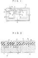
- Fig. 1 shows an LSI chip 1 having LSI-chip equivalent regions 2 and 3 according to a first embodiment of the present invention.
- the LSI-chip equivalent regions 2 and 3 have substantially the same patterns and functions as two LSIs which are separately prepared and which have evaluated and proven functions. Therefore, a plurality of external lead contacts 4 and 5, which are constituted by bonding pads originally used for connecting external regions with the LSI devices, and an intra-region wiring layer (not shown) are formed in each of the LSI-chip equivalent regions 2 and 3.
- a plurality of outer bonding pads 6 are formed in the peripheral portion of the chip 1 so as to connect the LSI devices with the external devices. Parts of the external lead contacts and the outer bonding pads are illustrated in Fig. 1.
- the necessary number of external lead contacts and outer bonding pads are formed in the peripheral portions of the LSI-chip equivalent regions 2 and 3 and in the peripheral portion of the chip 1.
- an external lead contact 4 1 in the chip equivalent region 2 is connected to an external lead contact 5, in the chip equivalent region 3 through a second wiring layer 7 made of polysilicon or aluminum, so that the chip equivalent region 2 can exchange a signal with the chip equivalent region 3 through the second wiring layer 7.
- the second wiring layer 7 is a substitute for a printed wire in the conventional printed wiring board.
- the second wiring layer 7 is formed in the process wherein the intra-region wiring layers (not shown) are formed in the chip equivalent regions 2 and 3.
- the second wiring layer 7 cannot be formed inside the regions 2 and 3, and a wiring region 9 is required to form the second wiring layer 7 between the chip equivalent regions 2 and 3.
- a wiring region 9 is required to form the second wiring layer 7 between the chip equivalent regions 2 and 3.
- an external lead contact 4 2 in the chip equivalent region 2 is connected to an outer bonding pad 6 1 through a second wiring layer 8 made of polysilicon or aluminum.
- the LSI chip according to the present invention can be prepared by using LSI patterns whose functions are already evaluated and proven.
- the manufacturing of the first embodiment will be exemplified by a MOS transistor and briefly described with reference to Fig. 2.
- Polysilicon is deposited on an oxide film 13 and is etched to give a predetermined pattern, thereby forming a gate electrode 14.
- a second wiring layer e.g., 7 in Fig. 1
- a second wiring layer e.g., 7 in Fig. 1
- a second wiring layer which crosses two or more second wiring layers
- an n-type impurity is diffused although it is not illustrated in Fig. 2.
- an oxide film 16 is formed to cover the entire surface, it is selectively etched to form a contact hole, and aluminum is deposited to cover the contact hole.
- the aluminum layer is selectively etched to give a predetermined pattern and to form an intra-region wiring layer 17, a second wiring layer 7 1 , and another second wiring layer 7 2 which crosses the second wiring layer 7" if required.
- the second wiring layer for connecting the external lead contacts and the outer bonding pads is simultaneously formed although it is not illustrated in Fig. 2.
- the second embodiment includes a two-layer wiring structure wherein an insulating film is formed between the intra-region wiring layer of the chip and the second wiring layer.
- a single chip 20 has two chip equivalent regions 21 and 22 with substantially the same functions and patterns as those of the LSIs separately formed with already evaluated, proven functions.
- Each of the chip equivalent regions 21 and 22 has intra-region wiring layers (not shown) of the corresponding original LSI.
- a plurality of external lead contacts 23 and 24 constituted by the bonding pads of the original LSls are formed in the peripheral portions of the chip equivalent regions 21 and 22, respectively.
- a plurality of outer bonding pads 25 are formed in the peripheral portion of the chip 20 so as to allow signal exchanges between the LSIs and their external devices.
- the external lead contacts 23 and 24 and the outer bonding pads 25 are generally formed of aluminum.
- a predetermined number of external lead contacts 23 and 24 and a predetermined number of outer bonding pads 25 are formed.
- Several external lead contacts (e.g. 23 i ) in the chip equivalent region 21 are connected to the corresponding external lead contacts (e.g., 24 1 ) through a second wiring layer 26 so as to exchange a signal therebetween.
- an oxide film is formed on the intra-region wiring layer which is regarded as a first aluminum layer.
- a second aluminum layer is formed on the oxide film to constitute the second wiring layer 26.
- the second wiring layer 26 can be formed on the chip equivalent regions 21 and 22.
- some of the external lead contacts 23 and 24 in the chip equivalent regions 21 and 22 are connected to the corresponding outer bonding pad 25 through another second wiring layer 27.
- the second wiring layer 27 is made of aluminum and can be formed in the process wherein the second aluminum layer is formed.
- the original bonding pads of each of the LSI chips are used as the external lead contacts.
- the bonding pads can be used as the external lead contacts with/without modification.
- a portion 4' used as a bonding pad of a given LSI chip is used as the external lead contact without modification and can be connected to a second wiring layer 8' through a via-contact.
- the original pattern can be used without modification, so that a new LSI design can be easily produced.
- a portion 4' (dotted portion) originally used as the bonding pad is modified to form an external lead contact 4" (hatched portion) having a different shape to that of the portion 4'.
- the original bonding pad and its vicinity can be modified to decrease the size of the resultant chip.
- Fig. 6 shows a complementary MOSFET (to be referred to as a CMOSFET hereafter) as an example.
- the present invention can be effectively applied to mount the LSI device in one package with limited power consumption since the CMOS has a low power consumption.
- a p-type impurity is diffused in an n-type semiconductor substrate 30 in accordance with a known technique to form a p-well layer 31 for the n-channel transistor. Thereafter, a polysilicon layer is deposited by a known technique and is selectively etched to form gate electrodes 36 and 37 for the transistors of the CMOSFET. Then a p-type impurity is diffused in an n-type semiconductor substrate 30 by a known technique to form the p-channel transistor's source 33 and drain 32.
- the n-channet transistor's source 34 and drain 35 are formed in a said p-well.
- a first aluminum wiring layer 38 as an intra-region wiring layer, is formed by a known method.
- an insulating film 39 such as a silicon oxide film is deposited to cover the entire surface and is selectively etched by photoengraving to form a contact hole 41 so as to connect the external lead contact 40 to a second aluminum wiring layer 42 in the subsequent process.
- the second aluminum wiring layer 42 is formed to connect to the underlying layer (i.e., external lead contact 40) through the via-contact 41.
- the second aluminum wiring layer 42 corresponds to the second wiring layer 26 (Fig.
- the external lead contact 40 corresponds to that denoted by 23 or 24 in Fig. 5. It should be noted that the via-contact need not be formed on the external lead contact.
- the second aluminum wiring layer can be formed on the first aluminum wiring layer, as the intra-region wiring layer, through the insulating interlayer. Therefore, unlike in the first embodiment, a special wiring region need not be provided, and the chip size can thus be reduced. In addition, since the first aluminum wiring layer does not cross the second aluminum wiring layer on the same plane, free circuit design can be performed. Furthermore, unlike in the first embodiment, polysilicon need not be used to constitute the intersection of the wiring layers. An electrical resistance of the intersection can be decreased, thereby preparing a high-speed LSI device.
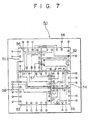
- Fig. 7 is a schematic plan view of an LSI device 50 which has the same construction as the device of the second embodiment and which can be suitably used in a microcomputer.
- five chip equivalent regions 51, 52, 53, 54 and 55 are formed on a single semiconductor substrate.
- the number of the chip equivalent regions is not limited to five, but can change in accordance with the system configuration of the microcomputer. More than one identical chip equivalent region may be formed.
- Each of the chip equivalent regions 51, 52, 53, 54 and 55 has substantially the same pattern as that of a corresponding LSI whose function is already evaluated and proven. In other words, a plurality of LSI patterns whose functions are evaluated and proven are electrophotographically printed on a single semiconductor substrate.
- the shape of the original bonding pads can change in a prescribed manner. Therefore, unlike the conventional LSI chip, the bonding pads of the original, separate chips are modified in shape and reduced in area to constitute external lead contacts (e.g., 56 and 57) in the chip equivalent regions 51, 52, 53, 54 and 55. In addition, bonding pads, i.e. outer bonding pads 58 used for input/output signal exchange, are formed in a peripheral portion of the chip 50.
- the present invention is not limited to the particular embodiments described above. Various changes and modifications which are obvious to those skilled in the art may be made within the spirit and scope of the present invention.
- the present invention may be applied to an aluminum gate-type transistor, a tungsten gate-type transistor, and a molybdenum gate-type transistor, in addition to the silicon gate-type transistor described above.
- the wiring material is not limited to aluminum, but can be extended to tungsten, molybdenum, or the like.
- the outer bonding pads are formed outside each chip equivalent region. However, if it is possible in the circuit design, the outer bonding pads may be formed on the external lead contacts of the chip equivalent regions through an insulating film.
- the second embodiment having a two-layer aluminum structure is disclosed above; however, a multilayer structure having three or more layers can be utilized.
- the bonding pads of the original IC chip can be used as the external lead contacts.
- the external lead contact has at least an electrode function which allows signal exchanges within a resultant LSI and a function which allows circuit operation within the chip equivalent region. Therefore, the external lead contact need not have a large area like the original bonding pad. It is preferred that the original bonding pad is decreased in size to constitute the external lead contact.
Landscapes
- Engineering & Computer Science (AREA)
- Physics & Mathematics (AREA)
- Power Engineering (AREA)
- Condensed Matter Physics & Semiconductors (AREA)
- General Physics & Mathematics (AREA)
- Computer Hardware Design (AREA)
- Microelectronics & Electronic Packaging (AREA)
- General Engineering & Computer Science (AREA)
- Geometry (AREA)
- Internal Circuitry In Semiconductor Integrated Circuit Devices (AREA)
- Semiconductor Integrated Circuits (AREA)
- Design And Manufacture Of Integrated Circuits (AREA)
Claims (10)
Applications Claiming Priority (4)
| Application Number | Priority Date | Filing Date | Title |
|---|---|---|---|
| JP9100283A JPS59215743A (ja) | 1983-05-24 | 1983-05-24 | 大規模集積回路装置 |
| JP9100383A JPS59215744A (ja) | 1983-05-24 | 1983-05-24 | 大規模集積回路装置 |
| JP91003/83 | 1983-05-24 | ||
| JP91002/83 | 1983-05-24 |
Publications (3)
| Publication Number | Publication Date |
|---|---|
| EP0127100A2 EP0127100A2 (de) | 1984-12-05 |
| EP0127100A3 EP0127100A3 (en) | 1986-08-27 |
| EP0127100B1 true EP0127100B1 (de) | 1990-04-11 |
Family
ID=26432403
Family Applications (1)
| Application Number | Title | Priority Date | Filing Date |
|---|---|---|---|
| EP84105778A Expired - Lifetime EP0127100B1 (de) | 1983-05-24 | 1984-05-21 | Integrierte Halbleiterschaltungsanordnung |
Country Status (3)
| Country | Link |
|---|---|
| US (1) | US4688070A (de) |
| EP (1) | EP0127100B1 (de) |
| DE (1) | DE3481958D1 (de) |
Families Citing this family (15)
| Publication number | Priority date | Publication date | Assignee | Title |
|---|---|---|---|---|
| JPH0673363B2 (ja) * | 1984-07-02 | 1994-09-14 | 株式会社東芝 | システムlsiの設計方法 |
| US4858175A (en) * | 1984-09-29 | 1989-08-15 | Kabushiki Kaisha Toshiba | Monolithic semi-custom IC having standard LSI sections and coupling gate array sections |
| JPS61222148A (ja) * | 1985-03-08 | 1986-10-02 | Fujitsu Ltd | 1チツプマイクロコンピユ−タの製造方法 |
| EP0204177A1 (de) * | 1985-05-31 | 1986-12-10 | Siemens Aktiengesellschaft | Anschlussanordnung für einen integrierten Halbleiterschaltkreis |
| US4910574A (en) * | 1987-04-30 | 1990-03-20 | Ibm Corporation | Porous circuit macro for semiconductor integrated circuits |
| US4990996A (en) * | 1987-12-18 | 1991-02-05 | Zilog, Inc. | Bonding pad scheme |
| US5014110A (en) * | 1988-06-03 | 1991-05-07 | Mitsubishi Denki Kabushiki Kaisha | Wiring structures for semiconductor memory device |
| JP2666807B2 (ja) * | 1988-06-16 | 1997-10-22 | 富士通株式会社 | 集積回路パターンの形成方法 |
| JP2585799B2 (ja) * | 1989-06-30 | 1997-02-26 | 株式会社東芝 | 半導体メモリ装置及びそのバーンイン方法 |
| JPH03142934A (ja) * | 1989-10-30 | 1991-06-18 | Mitsubishi Electric Corp | 半導体集積回路装置の配線接続構造 |
| US5119158A (en) * | 1989-11-21 | 1992-06-02 | Nec Corporation | Gate array semiconductor integrated circuit device |
| US5216280A (en) * | 1989-12-02 | 1993-06-01 | Kabushiki Kaisha Toshiba | Semiconductor integrated circuit device having pads at periphery of semiconductor chip |
| JP3150020B2 (ja) * | 1993-09-03 | 2001-03-26 | 日本電気アイシーマイコンシステム株式会社 | 半導体集積回路 |
| JP2000067102A (ja) * | 1998-08-18 | 2000-03-03 | Hitachi Ltd | 半導体集積回路の階層配線方法 |
| JP2003099414A (ja) * | 2001-09-21 | 2003-04-04 | Mitsubishi Electric Corp | 半導体集積回路 |
Family Cites Families (7)
| Publication number | Priority date | Publication date | Assignee | Title |
|---|---|---|---|---|
| US3518751A (en) * | 1967-05-25 | 1970-07-07 | Hughes Aircraft Co | Electrical connection and/or mounting arrays for integrated circuit chips |
| US3839781A (en) * | 1971-04-21 | 1974-10-08 | Signetics Corp | Method for discretionary scribing and breaking semiconductor wafers for yield improvement |
| US4234888A (en) * | 1973-07-26 | 1980-11-18 | Hughes Aircraft Company | Multi-level large scale complex integrated circuit having functional interconnected circuit routed to master patterns |
| JPS5636148A (en) * | 1979-08-31 | 1981-04-09 | Fujitsu Ltd | Semiconductor device and its manufacture |
| JPS5778146A (en) * | 1980-11-04 | 1982-05-15 | Hitachi Ltd | Integrated circuit device |
| JPS587847A (ja) * | 1981-07-07 | 1983-01-17 | Nec Corp | 半導体装置 |
| JPS5898938A (ja) * | 1981-12-09 | 1983-06-13 | Nec Corp | 半導体集積回路 |
-
1984
- 1984-05-21 EP EP84105778A patent/EP0127100B1/de not_active Expired - Lifetime
- 1984-05-21 DE DE8484105778T patent/DE3481958D1/de not_active Expired - Lifetime
- 1984-05-23 US US06/613,302 patent/US4688070A/en not_active Expired - Lifetime
Non-Patent Citations (1)
| Title |
|---|
| PATENTS ABSTRACTS OF JAPAN, vol. 7, no. 80 (E-168) [1225], 2nd April 1983; & JP - A - 58 7847 (NIPPON DENKI K.K.) 17-01-1983 * |
Also Published As
| Publication number | Publication date |
|---|---|
| EP0127100A3 (en) | 1986-08-27 |
| DE3481958D1 (de) | 1990-05-17 |
| EP0127100A2 (de) | 1984-12-05 |
| US4688070A (en) | 1987-08-18 |
Similar Documents
| Publication | Publication Date | Title |
|---|---|---|
| EP0127100B1 (de) | Integrierte Halbleiterschaltungsanordnung | |
| KR910000155B1 (ko) | 반도체 집적회로장치 및 그 제조방법 | |
| US5721151A (en) | Method of fabricating a gate array integrated circuit including interconnectable macro-arrays | |
| EP0093003B1 (de) | Gattermatrix für hochintegrierte Schaltungsanordnungen | |
| US4525809A (en) | Integrated circuit | |
| US5892276A (en) | Semiconductor integrated circuit | |
| US5060046A (en) | Semiconductor integrated circuit device having enlarged cells formed on ends of basic cell arrays | |
| JP3917683B2 (ja) | 半導体集積回路装置 | |
| JPH07111971B2 (ja) | 集積回路装置の製造方法 | |
| US4992845A (en) | Semiconductor integrated circuit device having input/output buffer cells each comprising a plurality of transistor regions arranged in a single line | |
| JPH0434309B2 (de) | ||
| EP0431490B1 (de) | Integrierte Halbleiterschaltungsvorrichtung mit Kontaktierungsflächen am Rande des Halbleiterchips | |
| EP0119059B1 (de) | Integrierte Halbleiterschaltung mit Gattermatrixstruktur | |
| US5206529A (en) | Semiconductor integrated circuit device | |
| US5171701A (en) | Method of manufacturing master-slice semiconductor integrated circuits | |
| JPS63142656A (ja) | セミカスタム半導体集積回路 | |
| JPH0120536B2 (de) | ||
| JPH0252428B2 (de) | ||
| JP2752262B2 (ja) | 1チップlsiの製造方法 | |
| JPH0371789B2 (de) | ||
| JP3636523B2 (ja) | 半導体集積回路装置およびその製造方法 | |
| EP0318869A1 (de) | Substratpotentialdetektionsschaltung | |
| JPH09205150A (ja) | 大規模集積回路装置の製造方法 | |
| JPH053252A (ja) | 半導体集積回路装置 | |
| JPH0566737B2 (de) |
Legal Events
| Date | Code | Title | Description |
|---|---|---|---|
| PUAI | Public reference made under article 153(3) epc to a published international application that has entered the european phase |
Free format text: ORIGINAL CODE: 0009012 |
|
| 17P | Request for examination filed |
Effective date: 19840615 |
|
| AK | Designated contracting states |
Designated state(s): DE FR GB IT |
|
| PUAL | Search report despatched |
Free format text: ORIGINAL CODE: 0009013 |
|
| AK | Designated contracting states |
Kind code of ref document: A3 Designated state(s): DE FR GB IT |
|
| 17Q | First examination report despatched |
Effective date: 19881020 |
|
| GRAA | (expected) grant |
Free format text: ORIGINAL CODE: 0009210 |
|
| AK | Designated contracting states |
Kind code of ref document: B1 Designated state(s): DE FR GB IT |
|
| ITF | It: translation for a ep patent filed |
Owner name: JACOBACCI & PERANI S.P.A. |
|
| ET | Fr: translation filed | ||
| REF | Corresponds to: |
Ref document number: 3481958 Country of ref document: DE Date of ref document: 19900517 |
|
| PLBE | No opposition filed within time limit |
Free format text: ORIGINAL CODE: 0009261 |
|
| STAA | Information on the status of an ep patent application or granted ep patent |
Free format text: STATUS: NO OPPOSITION FILED WITHIN TIME LIMIT |
|
| 26N | No opposition filed | ||
| ITTA | It: last paid annual fee | ||
| REG | Reference to a national code |
Ref country code: GB Ref legal event code: 746 Effective date: 19981012 |
|
| REG | Reference to a national code |
Ref country code: FR Ref legal event code: D6 |
|
| REG | Reference to a national code |
Ref country code: GB Ref legal event code: IF02 |
|
| PGFP | Annual fee paid to national office [announced via postgrant information from national office to epo] |
Ref country code: FR Payment date: 20030508 Year of fee payment: 20 |
|
| PGFP | Annual fee paid to national office [announced via postgrant information from national office to epo] |
Ref country code: GB Payment date: 20030519 Year of fee payment: 20 |
|
| PGFP | Annual fee paid to national office [announced via postgrant information from national office to epo] |
Ref country code: DE Payment date: 20030529 Year of fee payment: 20 |
|
| PG25 | Lapsed in a contracting state [announced via postgrant information from national office to epo] |
Ref country code: GB Free format text: LAPSE BECAUSE OF EXPIRATION OF PROTECTION Effective date: 20040520 |
|
| REG | Reference to a national code |
Ref country code: GB Ref legal event code: PE20 |