EP0108336A2 - Spannungsgerät mit hochfrequenter Speisung für Röntgenstrahlerzeuger - Google Patents
Spannungsgerät mit hochfrequenter Speisung für Röntgenstrahlerzeuger Download PDFInfo
- Publication number
- EP0108336A2 EP0108336A2 EP83110660A EP83110660A EP0108336A2 EP 0108336 A2 EP0108336 A2 EP 0108336A2 EP 83110660 A EP83110660 A EP 83110660A EP 83110660 A EP83110660 A EP 83110660A EP 0108336 A2 EP0108336 A2 EP 0108336A2
- Authority
- EP
- European Patent Office
- Prior art keywords
- voltage
- transformer
- inverter
- converter
- output
- Prior art date
- Legal status (The legal status is an assumption and is not a legal conclusion. Google has not performed a legal analysis and makes no representation as to the accuracy of the status listed.)
- Granted
Links
Images


Classifications
-
- H—ELECTRICITY
- H02—GENERATION; CONVERSION OR DISTRIBUTION OF ELECTRIC POWER
- H02M—APPARATUS FOR CONVERSION BETWEEN AC AND AC, BETWEEN AC AND DC, OR BETWEEN DC AND DC, AND FOR USE WITH MAINS OR SIMILAR POWER SUPPLY SYSTEMS; CONVERSION OF DC OR AC INPUT POWER INTO SURGE OUTPUT POWER; CONTROL OR REGULATION THEREOF
- H02M3/00—Conversion of dc power input into dc power output
- H02M3/22—Conversion of dc power input into dc power output with intermediate conversion into ac
- H02M3/24—Conversion of dc power input into dc power output with intermediate conversion into ac by static converters
- H02M3/28—Conversion of dc power input into dc power output with intermediate conversion into ac by static converters using discharge tubes with control electrode or semiconductor devices with control electrode to produce the intermediate ac
- H02M3/325—Conversion of dc power input into dc power output with intermediate conversion into ac by static converters using discharge tubes with control electrode or semiconductor devices with control electrode to produce the intermediate ac using devices of a triode or a transistor type requiring continuous application of a control signal
- H02M3/335—Conversion of dc power input into dc power output with intermediate conversion into ac by static converters using discharge tubes with control electrode or semiconductor devices with control electrode to produce the intermediate ac using devices of a triode or a transistor type requiring continuous application of a control signal using semiconductor devices only
- H02M3/337—Conversion of dc power input into dc power output with intermediate conversion into ac by static converters using discharge tubes with control electrode or semiconductor devices with control electrode to produce the intermediate ac using devices of a triode or a transistor type requiring continuous application of a control signal using semiconductor devices only in push-pull configuration
- H02M3/3376—Conversion of dc power input into dc power output with intermediate conversion into ac by static converters using discharge tubes with control electrode or semiconductor devices with control electrode to produce the intermediate ac using devices of a triode or a transistor type requiring continuous application of a control signal using semiconductor devices only in push-pull configuration with automatic control of output voltage or current
-
- H—ELECTRICITY
- H05—ELECTRIC TECHNIQUES NOT OTHERWISE PROVIDED FOR
- H05G—X-RAY TECHNIQUE
- H05G1/00—X-ray apparatus involving X-ray tubes; Circuits therefor
- H05G1/08—Electrical details
- H05G1/10—Power supply arrangements for feeding the X-ray tube
- H05G1/20—Power supply arrangements for feeding the X-ray tube with high-frequency ac; with pulse trains
-
- H—ELECTRICITY
- H05—ELECTRIC TECHNIQUES NOT OTHERWISE PROVIDED FOR
- H05G—X-RAY TECHNIQUE
- H05G1/00—X-ray apparatus involving X-ray tubes; Circuits therefor
- H05G1/08—Electrical details
- H05G1/26—Measuring, controlling or protecting
- H05G1/30—Controlling
- H05G1/32—Supply voltage of the X-ray apparatus or tube
-
- Y—GENERAL TAGGING OF NEW TECHNOLOGICAL DEVELOPMENTS; GENERAL TAGGING OF CROSS-SECTIONAL TECHNOLOGIES SPANNING OVER SEVERAL SECTIONS OF THE IPC; TECHNICAL SUBJECTS COVERED BY FORMER USPC CROSS-REFERENCE ART COLLECTIONS [XRACs] AND DIGESTS
- Y02—TECHNOLOGIES OR APPLICATIONS FOR MITIGATION OR ADAPTATION AGAINST CLIMATE CHANGE
- Y02B—CLIMATE CHANGE MITIGATION TECHNOLOGIES RELATED TO BUILDINGS, e.g. HOUSING, HOUSE APPLIANCES OR RELATED END-USER APPLICATIONS
- Y02B70/00—Technologies for an efficient end-user side electric power management and consumption
- Y02B70/10—Technologies improving the efficiency by using switched-mode power supplies [SMPS], i.e. efficient power electronics conversion e.g. power factor correction or reduction of losses in power supplies or efficient standby modes
Definitions
- This invention relates to adjustable high voltage power supplies and more particularly dc-dc resonant converters suitable for powering x-ray tubes.
- High voltage adjustable power supplies with a power output from a few hundred watts for applications such as dental x-rays to the 100 kilowatt range for diagnostic modalities such as computer tomography and x-ray fluorography, are used to energize x-ray tubes.
- a power supply with low weight, low output ripple to reduce filtering requirements and fast speed of response to accurately set exposures is desirable.
- Conventional power supplies of the single and three phase versions for energizing x-ray tubes use 60 Hertz adjustable autotransformers to supply adjustable voltages to a step-up 60 Hertz transformer.
- the 60 Hertz transformers are bulky and the prior art circuits have high output ripple and slow response.
- U. S . patent 4,295,449, of Ebersberger et al discloses a resonant circuit using silicon controlled rectifiers (SCRs).
- SCRs silicon controlled rectifiers
- the resonant circuit is not configured to take advantage of the capacitance built into the transformer.
- voltage control is achieved by a phase controlled rectifier front end since only limited voltage control can be achieved by lowering the SCRs frequency. The frequency can only be lowered from resonance and not raised above resonance since a leading load is needed to maintain SCR commutation. Operation at frequencies below resonance results in increased output ripple and requires the transformer to be designed for the lowest operating frequency to be encountered. The lower the frequency the larger the reactive components required.
- a dc to ac voltage step-up step-down converter having a first means for supplying ac output power at a commanded frequency from dc input power.
- a transformer receives the ac power from the first means and provides a transformed ac output voltage.
- a control responsive to a commanded voltage magnitude provides a frequency command to the first means to adjust the input frequency to the transformer and thereby control the output voltage of the transformer.
- the frequency of power supplied to the transformer is selected to cause the transformer shunt capacitance and leakage inductance to resonate and achieve voltage transformation due to the turns ratio of the transformer and the resonant change in voltage across the shunt capacitance of the resonant circuit.
- a high voltage dc to dc resonant converter having a voltage input inverter feeding a high frequency transformer.
- the output of the transformer is connected to a rectifier circuit which provides high voltage dc to a load.
- the transformer is supplied high frequency square waves of voltage from the inverter which operates at or above the transformer's shunt capacitance and leakage reactance damped resonant frequency. Voltage step up in the converter is due to the turns ratio of the transformer and the resonant rise in voltage across the shunt capacitance of the resonant circuit.
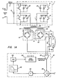
- FIG. 1A a resonant dc to dc converter.
- DC power is provided from an external source (not shown) at terminals 3 and 4.
- a 120 cycle inductive filter 6 Connected between terminal 3 and one end of a high frequency capacitance filter 5 is a 120 cycle inductive filter 6. The other end of capacitance filter 5 is connected to terminal 4.
- a full bridge inverter 7 is provided having four switching devices that are capable of carrying reverse current and capable of being turned off by a switching signal.
- the switching devices are shown as bipolar junction power transistors 9, 11, 13 and 15 each having an inverse diode 17, 19, 21 and 23 connected in parallel, respectively.
- MOSFETs power metal-oxide semiconductor field effect transistors
- monolithic Darlingtons reverse current carried by a parasitic diode
- gate turn-off silicon controlled rectifiers each in inverse parallel with a diode.
- Power transistors 9 and 11 are connected in series with one another across capacitor 5 as are power transistors 13 and 15.
- the output of inverter 7 is available across the junctions a and b between series connected transistors 9 and 11, and series connected transistors 13 and 15, respectively.
- Snubbers comprising snubber capacitors 25, 27, 29 and 31 are each connected across respective transistors 9, 11, 13 and 15.
- the transformer 35 has two secondary windings 37 and 39.
- a high voltage full bridge diode rectifier 41 is connected across secondary winding 37 and a high voltage full bridge diode rectifier 43 is connected across the secondary winding 39.
- the outputs of the two bridge rectifiers 41 and 43 are connected in series with one another, with the junction of the two rectifiers grounded to reduce insulation to ground requirements of the transformer and to facilitate voltage and current measurement for control purposes.
- the two rectifiers supply a load shown in Figure 1A as an x-ray tube 45.
- a control 47 has as an input a commanded dc voltage E for the dc-dc converter and a feedback output voltage signal proportional to E 0 .
- the output voltage signal is obtained from a voltage divider comprising four resistors 49, 50, 51 and 52 connected in series with one another, with the series combination connected across the x-ray tube 45. The junction between resistors 50 and 51 is grounded and the output of the voltage divider is taken across resistors 49 and 50.
- the output voltage of the voltage divider is coupled to a differential amplifier 53 (the output voltage of the voltage divider between resistors 49 and 50 is positive relative to ground, and the output voltage between resistors 51 and 52 is negative relative to ground) producing a signal proportional to the output voltage.
- the commanded voltage is compared to the signal proportional to the actual output voltage E in a summer 58 to generate an error signal.
- the error signal is passed through a proportional plus integral regulator 60 to a limit circuit 62.
- the regulator 60 shown does not invert the signal.
- the limit circuit 62 assures that a lagging load is presented to the inverter by allowing the inverter to operate at or above the resonant frequency of the series resonant circuit.
- the output of the limit circuit is connected to a voltage controlled oscillator 64 which provides input signals to base driver 66 to alternately switch the transistors at opposite corners of the inverter 7.
- the equivalent circuit has a primary leakage inductance L p connected in series with a magnetizing inductance of the entire core referred to the primary, L m .
- the magnetizing inductance L m is in parallel with the primary winding of an ideal transformer having two secondary windings. Connected in series with the first secondary winding is the leakage inductance of the first secondary L s1 and the shunt capacitance of the first secondary C l .
- the leakage inductance of the second secondary winding L s2 is in series with the shunt capacitance of the second secondary winding C 2 .
- the effective shunt capacitance is defined as the sum of all distributed internal and external capacitances of a coil as reflected to the coil terminals. It is that capacitance which, when connected across an equivalent ideal coil of zero capacitance represents all of the capacitances of the real coil lumped into a single capacitance.
- the outputs of the equivalent circuit are available across each of the equivalent shunt capacitors C l and C 2 , respectively.
- the magnetizing inductance L m is much greater than the primary leakage inductance Lp and secondary leakage inductances L s1 and L s2 , respectively.
- the magnetizing inductance can be neglected leaving an equivalent circuit of leakage inductance of the primary in series with the parallel combination of the secondary inductance in series with the parallel combination of the shunt capacitors.
- the resonating circuit of Figure 1A is realized with parasitic elements, with the transformer leakage reactances serving as the resonating inductor while the shunt capacitance serves as the resonating capacitance.
- a commanded dc output voltage E is compared in summer 58 to a signal proportional to the actual output voltage E o to develop an error signal.
- the error signal after passing through the proportional plus integral regulator circuit 60, is supplied to an input of the limit circuit 62.
- the limit circuit provides a maximum output signal in response to a minimum error signal.
- the maximum output signal of the limit circuit when provided to the voltage control oscillator 64 results in a signal supplied to the base drivers 66 which in turn switches the transistors 9, 11, 13 and 15 of the inverter 7.
- the inverter drives the series resonant circuit of parasitic elements of the transformer above its resonant frequency.
- the limit circuit 62 decreases the voltage supplied to the voltage control oscillator, thereby decreasing the frequency of the signal supplied to the parasitic resonant circuit causing the circuit to operate closer to its damped resonant frequency.
- the voltage ratio of the input voltage to the output voltage versus inverter frequency is shown for several normalized load impedances where the normalized load impedance R o is expressed by the equation where R is the load resistance connected to the resonant circuit and L and C are the effective inductance and capacitance of the parasitic resonant circuit, respectively.
- R is the load resistance connected to the resonant circuit
- L and C are the effective inductance and capacitance of the parasitic resonant circuit, respectively.
- An increase in the normalized resistance R o ' results in a decrease in the damping since the load resistance is connected in parallel with the shunt capacitance of the resonant circuit.
- Maximum step-up occurs with minimum damping at the damped resonant frequency which is slightly lower than the resonant frequency of the parasitic circuit.
- the resonant frequency F is defined by
- a resonant frequency ratio of 1 signifies that the actual frequency F which is in the numerator is equal to the resonant frequency F in the denominator.
- the converter is capable of voltage step-up and voltage step-down operation dependent on the turns ratio and is always operated above the damped resonant frequency to assure that the parasitic resonant components present a lagging load to the inverter.
- the voltage developed across the individual energy storage elements in the series resonant circuit is dependent on the damping provided by the rectifier, filter and the tube, and the frequency of operation.
- the voltage across one series energy storage element can be greater than the voltage across the series combination of the resonant circuit elements.
- High instantaneous voltages across the inductance and capacitance occur 180° out of phase with one another.
- the output voltage of the resonant circuit is taken across the equivalent shunt capacitance of the resonant circuit of the transformer parasitic series resonant circuit.
- the voltage step up and step down as plotted against resonant frequency ratio F/F in Figure 2 is measured across the capacitor in a series resonant circuit.
- the resonant rise in voltage across each of the reactive elements in the series resonant circuit for a given value of current is Q times the applied voltage.
- Q is the quality factor, a dimensionless ratio of the maximum energy stored to the energy dissipated per cycle, times a constant.
- the amount of voltage step-up provided by the converter is dependent on the step-up ratio of the transformer used and on the high voltages developed across the capacitor of the resonant circuit.
- the total step-up of the converter is the product of the turns ratio times the step up or step down due to the resonant circuit.
- Frequency control can result in a step-up greater or less than the turns ratio of the transformer 35 in the circuit of Figure lA.
- the closed loop control 47 adjusts the frequency at which the transistors are switched to achieve the voltage step-up needed to obtain the desired output voltage. Since the transformer is operating at frequencies much higher than 60 Hz, fast response to changes in commanded voltages can be achieved.
- the gate drivers switch transistors at opposite corners of the inverter, resulting in square waves of voltage V ab supplied to the transformer primary as shown in Figure 3A.
- the voltage across, and the current flowing in, a transistor in the circuit of Figure 1A is shown in Figures 3B and 3C, respectively.
- the square waves of voltage from the inverter result in approximately sinusoidal currents flowing through the parasitic resonant circuit which should result in easier electromagnetic interference filtering.
- the current drawn by transformer 35 in the circuit of Figure lA is shown in Figure 3D and the voltage waveform across a secondary of the transformer, which corresponds to the voltage across one of the capacitors in Figure 1B, is shown in Figure 3E.
- the parasitic resonant circuit of transformer 35 is driven at a frequency such that a lagging load is presented to the inverter between junctions a and b, that is, the current i c lags the voltage V ab .
- the lagging load is obtained by operating the inverter at frequencies at or above the damped resonant frequency of the parasitic circuit.
- leakage inductance and shunt capacitance of high voltage, high turns ratio transformers can be determined after the transformers are built and the resonant frequency can then be determined from these measurements.
- the leakage inductance of the transformer can also be selected before building the transformer so that the leakage inductance (and hence leakage reactance), is a function of the geometry of the windings as well as the number of turns of the windings (leakage inductance increases as the square of the turns ratio).
- Leakage inductance can be increased by interposing a magnetic shunt between the primary and secondary of the transformer and by increasing the distance between primary and secondary windings. Shunt capacitance is also affected by the winding geometry.
- the winding geometry which provides minimum leakage inductance between two windings usually has the maximum shunt capacitance. Selection of the winding geometry and core structure can be used to provide particular values of leakage reactance and shunt capacitance which determine the resonant frequency and the frequency at or above which the circuit will operate. Capacitance is present due to the capacitance between the windings, of which they are a large number, and the multiplication of the secondary capacitances by the turns ratio when they are referred to the primary. The interconnection of the layers of windings in the transformer can be varied to adjust the distributed capacitance.
- the switching recovery time of the transistors in the circuit of Figure 1A limits the attainable switching frequencies. Higher frequencies (5-30 Kilohertz) permit smaller reactive components to be used.
- a snubber capacitor can be connected directly across the transistor without need for a current limiting resistor in series with the capacitor, resulting in reduced turn off dissipation of the transistor and lossless snubber action.
- the diodes in inverse parallel with the transistors can be of medium speed since there is no voltage increase immediately experienced by the diode after its turn-off. Rather, each transistor in parallel with a diode conducts, keeping the diode voltage low. Only after the transistor turns off is an increased voltage applied to the diode.
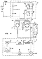
- FIG. 4 a half bridge arrangement of the present invention is shown.
- DC input power obtained from an external source (not shown) is connected through an inductor 75 to a half bridge inverter 77 comprising two capacitors 79 and 81 connected in series across the positive and negative rails of the dc input power to establish a split power supply.
- Two series connected switches capable of conducting reverse current are connected between the positive and negative rails of the half bridge inverter 77.
- the choice of switches is the same as in the circuit of Figure 1A.
- the switches shown are bipolar transistors 83 and 85 with inverse parallel diodes 87 and 89 connected across each switch, respectively.
- Lossless snubbers comprising capacitors 91 and 93 are each connected across the switches, respectively.
- the output of the half bridge inverter is available across the junctions between the series connected capacitors 79 and 81 and the two series connected switches.
- a high frequency transformer 35 Connected to the output of the half bridge inverter is a high frequency transformer 35 with two secondary windings 37 and 39, two diode bridges 41 and 43 and an x-ray tube 45 as in the circuit of Figure lA.
- the circuit of Figure 4 is controlled in the same manner as the circuit of Figure lA except that half as many gate drivers are needed.
- circuit of Figure 4 The operation of the circuit of Figure 4 is the same as that for the circuit of Figure 1A except that there are half as many switches and half as many gate drivers, but each of these devices must carry double current for the same output power.
- One half of the DC voltage from inductor 75 is applied to primary winding 33 as compared to the full bridge embodiment since the voltage between the capacitors 79 and 81 is fired at 1/2 the DC supply voltage.
- the circuit of Figure 4 has the advantage of inherently blocking any dc offset voltage which may result from unequal conduction drops or switching times of the semiconductors-since the load of the inverter is connected at one end between two series connected capacitors.
- Figure 5 illustrates a push-pull embodiment of the present invention.
- the positive terminal of an external dc power supply (not shown) is connected through an inductor 6 to one side of high frequency filter capacitor 5, the other side of which is connected to the negative rail of the dc supply which corresponds to the center tap of a center tapped primary winding 6 of transformer 97.
- An inverter 99 has a first switch with reverse current carrying ability connected between the positive output side of inductor 6 and one end of the primary winding 96 and a second switch connected between the positive output side of inductor 6 and the other end of the primary winding 96.
- the choice of switching devices is the same as for the circuit of Figure 1A.
- the first and second switches comprise bipolar transistors 101 and 102, respectively, each having a diode, 103 and 104, connected across it in inverse parallel, respectively.
- a lossless snubber comprising a capacitor 105 is connected across switch 101 and a lossless snubber comprising a capacitor 106 is connected across switch 102.
- the secondary windings 17 and 39 of transformer 97 are connected as in the circuit of Figure lA with two full bridge diode rectifiers 41 and 43 and an x-ray tube.
- the control 47 in the circuit of Figure 5 is the same as in the circuit of Figure lA except that only two gate drivers are needed.
- circuit of Figure 5 The operation of the circuit of Figure 5 is the same as that of the circuit of Figure lA, except that each switch has to block double the dc bus voltage.
- An advantage of the circuit of Figure 5 is the common connection point of the switches which eliminates the necessity for transformer coupling or opto-isolation between the base drivers and the switches.
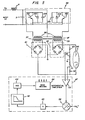
- FIG. 6 illustrates another embodiment of the present invention, which can supply two ranges of input voltage to a transformer primary winding.
- An external ac supply (not shown) is connected to a full bridge rectifier 111.
- the positive dc output of the rectifier is connected through an inductive filter 6 to a first capacitor 113 which is connected in series with a second capacitor 115.
- the second capacitor is connected to the negative output of the full bridge rectifier 111.
- Connected across the two capacitors is a full bridge inverter 117 having four switches with reverse current blocking ability.
- Each switch comprises a bipolar transistor 119, 120, 121 and 122 with an inverse parallel diode 123, 124, 125 and 126 connected across each transistor, respectively.
- Transistors 119 and 120 are connected in series in a first leg of inverter 117 and transistors 121 and 122 are connected in series in a second leg of the inverter.
- Lossless snubbers comprising capacitors 127, 128, 129 and 130 are connected across each transistor, respectively.
- the normally-open contacts 131 of a relay are connected across the junctions between the capacitors 113 and 115 and between transistors 119 and 120 of the first inverter leg.
- the output of the inverter 117 is available across the junctions between transistors 119 and 120, and between transistors 121 and 122.
- the output of the inverter is connected to the high frequency transformer primary as in the circuit of Figure lA.
- a switch 135 is connected in series with a pull up resistor 137.
- An external logic power source (not shown) provides an enabling signal to AND gates 139 and 141 when switch 135 is open, permitting a transistor switching signal from the base drivers to be connected through AND gate 139 to switch transistor 119 and switching signal connected through AND gate 141 to switch transistor 120.
- a signal inverter 143 keeps coil driving transistor 145 biased out of conduction.
- switch 135 is closed, AND gates 139 and 141 are disabled, preventing transistors 119 and 120 from receiving switching signals.
- Signal inverter 143 provides a logical one to the base of coil driving transistor 145 which in turn energizes the relay coil 131a by permitting power to flow from an external power source through the relay coil and through the transistor 145. Energizing the relay coil 131a causes its associated contacts 131 to close.
- a transient suppression network comprising a resistor 147 and a diode 149 is connected across the relay coil to provide a path for decay current when transistor 145 is turned off.
- Switch 131 can alternately be implemented with a triac using suitable control circuitry.
- the circuit of Figure 6 is controlled in the same manner as the circuit of Figure 1A except that closing switch 135 disables the base signals to transistor 119 and 120.
- a 6:1 voltage range adjustment is typically needed.
- the range may be achieved through frequency control alone by going to a higher frequency to reduce the voltage (see Figure 2) or, if it is desired to limit the upper frequency of operation, it is possible to adjust the input voltage to different levels.
- the x-ray exposure is determined prior to turning on the power supply. Therefore the relay contacts 131 do not have to make or break current since it is set by closing switch 135 before circuit operation commences.
- relay coil 131a is eneregized, closing contacts 131, so that the transistors 119 and 120 are not switched by the control circuit and the inverter operates as a half bridge inverter with only one-half the dc input voltage applied to the transformer primary 33.
- the switch 131 in the open position the circuit operates with a full bridge inverter with all transistor switches operating and the full dc input voltage applied to the transformer primary 33. Thus two ranges of output voltage are possible.
Applications Claiming Priority (2)
| Application Number | Priority Date | Filing Date | Title |
|---|---|---|---|
| US438828 | 1982-11-03 | ||
| US06/438,828 US4504895A (en) | 1982-11-03 | 1982-11-03 | Regulated dc-dc converter using a resonating transformer |
Publications (3)
| Publication Number | Publication Date |
|---|---|
| EP0108336A2 true EP0108336A2 (de) | 1984-05-16 |
| EP0108336A3 EP0108336A3 (en) | 1986-06-11 |
| EP0108336B1 EP0108336B1 (de) | 1990-05-23 |
Family
ID=23742193
Family Applications (1)
| Application Number | Title | Priority Date | Filing Date |
|---|---|---|---|
| EP83110660A Expired - Lifetime EP0108336B1 (de) | 1982-11-03 | 1983-10-26 | Spannungsgerät mit hochfrequenter Speisung für Röntgenstrahlerzeuger |
Country Status (5)
| Country | Link |
|---|---|
| US (1) | US4504895A (de) |
| EP (1) | EP0108336B1 (de) |
| JP (1) | JPS59103300A (de) |
| DE (1) | DE3381612D1 (de) |
| ES (1) | ES526933A0 (de) |
Cited By (18)
| Publication number | Priority date | Publication date | Assignee | Title |
|---|---|---|---|---|
| EP0138486A2 (de) * | 1983-09-29 | 1985-04-24 | Kabushiki Kaisha Toshiba | Impuls-Hochspannungsgerät für eine Röntgenröhre |
| EP0143657A2 (de) * | 1983-11-30 | 1985-06-05 | Kabushiki Kaisha Toshiba | Digitaler Röntgenaufnahmeapparat |
| EP0146855A2 (de) * | 1983-12-22 | 1985-07-03 | General Electric Company | Schutz vor einem Durchschlag bei einem Inverter eines Röntgen-Generators |
| EP0175139A1 (de) * | 1984-08-23 | 1986-03-26 | Heimann GmbH | Schaltungsanordnung zur Hochspannungsversorgung einer Röntgenröhre |
| DE3532629A1 (de) * | 1984-09-14 | 1986-03-27 | Kabushiki Kaisha Toshiba, Kawasaki, Kanagawa | Stromversorgungsschaltung des spannungsresonanztyps fuer eine roentgenroehre |
| EP0175811A1 (de) * | 1983-08-22 | 1986-04-02 | General Electric Company | Vollast-Leerlauf-Regelung für einen spannungsgespeisten Resonanzwechselrichter |
| EP0180750A1 (de) * | 1984-10-09 | 1986-05-14 | Siemens Aktiengesellschaft | Mittelfrequenz-Röntgengenerator |
| DE3546213A1 (de) * | 1984-12-28 | 1986-07-03 | Hitachi Medical Corp., Tokio/Tokyo | Wechselrichter-roentgenvorrichtung |
| GB2169424A (en) * | 1984-11-30 | 1986-07-09 | Rca Corp | Frequency controlled resonant regulator |
| EP0189775A1 (de) * | 1985-01-25 | 1986-08-06 | Heimann GmbH | Wechselrichter |
| FR2577373A1 (fr) * | 1985-02-12 | 1986-08-14 | Thomson Cgr | Alimentation haute tension continue, notamment pour emetteur de rayons x |
| US4823250A (en) * | 1987-11-05 | 1989-04-18 | Picker International, Inc. | Electronic control for light weight, portable x-ray system |
| EP0343855A2 (de) * | 1988-05-27 | 1989-11-29 | AT&T Corp. | Halbbrückenresonanzwandler mit Nullspannungsschaltung |
| EP0405399A3 (en) * | 1989-06-30 | 1991-06-05 | Kabushiki Kaisha Toshiba | X-ray generator apparatus |
| US5105351A (en) * | 1989-06-30 | 1992-04-14 | Kabushiki Kaisha Toshiba | X-ray power supply with plural frequency converters |
| EP0487766A1 (de) * | 1990-11-27 | 1992-06-03 | Siemens Aktiengesellschaft | Röntgendiagnostikgenerator mit einem seinen Hochspannungstransformator speisenden Wechselrichter |
| EP0612096A1 (de) * | 1993-02-17 | 1994-08-24 | Philips Patentverwaltung GmbH | Antriebsvorrichtung für eine Drehanode |
| EP0691801A1 (de) * | 1994-07-08 | 1996-01-10 | Hamamatsu Photonics K.K. | Röntgenstrahlenquelle |
Families Citing this family (122)
| Publication number | Priority date | Publication date | Assignee | Title |
|---|---|---|---|---|
| US5744915A (en) * | 1978-03-20 | 1998-04-28 | Nilssen; Ole K. | Electronic ballast for instant-start lamps |
| US4601051A (en) * | 1983-12-22 | 1986-07-15 | General Electric Company | Protective circuit for X-ray generator |
| JPS60152266A (ja) * | 1984-01-17 | 1985-08-10 | Hitachi Medical Corp | インバ−タ式スイツチング電源回路 |
| US4653082A (en) * | 1984-01-18 | 1987-03-24 | Kabushiki Kaisha Toshiba | High voltage generating device for X-ray apparatus |
| US6229718B1 (en) * | 1984-10-05 | 2001-05-08 | Ole K. Nilssen | Parallel-resonant bridge inverter |
| US4710860A (en) * | 1984-11-26 | 1987-12-01 | Kabushiki Kaisha Toshiba | Ripple-free DC high voltage generating apparatus for X-ray tube |
| US4695934A (en) * | 1985-05-13 | 1987-09-22 | General Electric Company | Multiple output resonant power supply |
| US4651267A (en) * | 1985-06-14 | 1987-03-17 | Sundstrand Corporation | Proportional base drive circuit for transistorized bridge inverter |
| DE3522569A1 (de) * | 1985-06-24 | 1987-01-02 | Metallgesellschaft Ag | Stromversorgung fuer ein elektrofilter |
| US4733137A (en) * | 1986-03-14 | 1988-03-22 | Walker Magnetics Group, Inc. | Ion nitriding power supply |
| JPS62250874A (ja) * | 1986-04-23 | 1987-10-31 | Fuji Electric Co Ltd | 直列共振負荷用電圧形インバ−タ |
| US4691275A (en) * | 1986-06-04 | 1987-09-01 | Superior Manufacturing & Instrument Corporation | Current fed inverter |
| US4864483A (en) * | 1986-09-25 | 1989-09-05 | Wisconsin Alumni Research Foundation | Static power conversion method and apparatus having essentially zero switching losses and clamped voltage levels |
| ES2003363A6 (es) * | 1986-10-02 | 1988-11-01 | Gh Ind Sa | Perfeccionamientos en generadores de alta frecuencia para aplicaciones de calentamiento por induccion laser plasma y similares |
| GB2196803B (en) * | 1986-10-24 | 1990-10-31 | Kyoei Densoku Co Ltd | High-frequency power supply output control arrangement |
| US4729085A (en) * | 1986-12-29 | 1988-03-01 | Rca Corporation | Frequency limited resonant regulator useful in, for example, a half-bridge inverter |
| JPH07118915B2 (ja) * | 1987-01-30 | 1995-12-18 | 株式会社日立メデイコ | 共振型dc−dcコンバ−タ |
| US4833584A (en) * | 1987-10-16 | 1989-05-23 | Wisconsin Alumni Research Foundation | Quasi-resonant current mode static power conversion method and apparatus |
| US5329220A (en) * | 1987-10-27 | 1994-07-12 | Hase A M | Shunt control |
| US4843202A (en) * | 1987-12-28 | 1989-06-27 | General Electric Company | Magnetron with frequency control for power regulation |
| DE3802231A1 (de) * | 1988-02-08 | 1989-07-27 | Jurij Alekseevic Spiridonov | Einrichtung zum regeln der magnetronleistung eines hhf-haushaltsofens |
| JPH01218365A (ja) * | 1988-02-25 | 1989-08-31 | Fanuc Ltd | インバータ装置 |
| US4864479A (en) * | 1988-03-07 | 1989-09-05 | General Electric Company | Full-bridge lossless switching converter |
| US4912622A (en) * | 1988-03-07 | 1990-03-27 | General Electric Company | Gate driver for a full-bridge lossless switching device |
| US4885671A (en) * | 1988-03-24 | 1989-12-05 | General Electric Company | Pulse-by-pulse current mode controlled power supply |
| US4853832A (en) * | 1988-08-01 | 1989-08-01 | University Of Toledo | Cascaded resonant bridge converters |
| US5014182A (en) * | 1989-04-19 | 1991-05-07 | Lambda Electronics Inc. | High frequency self-oscillating inverter with negligible switching losses |
| US5189602A (en) * | 1989-05-12 | 1993-02-23 | General Electric Cgr S.A. | High-voltage generator with selective half-bridge and full-bridge operation |
| US4930146A (en) * | 1989-07-10 | 1990-05-29 | General Electric Company | X-ray tube current control with constant loop gain |
| US4969076A (en) * | 1989-08-14 | 1990-11-06 | General Electric Company | Load compensating gain control for a series resonant inverter |
| JP2692765B2 (ja) * | 1989-12-22 | 1997-12-17 | 株式会社日立製作所 | ダイオード及びigbtとの並列回路とそのモジュール及びそれを用いた電力変換装置 |
| DE59005746D1 (de) * | 1990-02-07 | 1994-06-23 | Siemens Ag | Steuerverfahren und Steuersatz zur Dämpfung von Resonanzschwingungen eines Parallelschwingkreises für einen Pulswechselrichter eines Stromzwischenkreisumrichters. |
| US5187737A (en) * | 1990-08-27 | 1993-02-16 | Origin Electric Company, Limited | Power supply device for X-ray tube |
| US5291384A (en) * | 1991-06-20 | 1994-03-01 | Unitrode Corporation | Phase shifted switching controller |
| US5272618A (en) * | 1992-07-23 | 1993-12-21 | General Electric Company | Filament current regulator for an X-ray system |
| US5367448A (en) * | 1992-08-07 | 1994-11-22 | Carroll Lawrence B | Three phase AC to DC power converter |
| TW344190B (en) * | 1992-09-22 | 1998-11-01 | Matsushita Electric Works Ltd | Discharge lamp lighting device |
| US5594635A (en) * | 1993-03-30 | 1997-01-14 | Motorola, Inc. | Constant frequency, zero-voltage-switching converters with resonant switching bridge |
| US5532919A (en) * | 1993-03-30 | 1996-07-02 | Motorola, Inc. | Variable frequency, zero voltage switching, quasi-resonant converters with resonant bridge switch |
| US5420781A (en) * | 1993-09-02 | 1995-05-30 | General Electric Company | High voltage sensing circuit for an X-ray tube power supply |
| US5400385A (en) * | 1993-09-02 | 1995-03-21 | General Electric Company | High voltage power supply for an X-ray tube |
| DE4443551A1 (de) * | 1994-12-07 | 1996-06-20 | Philips Patentverwaltung | Anordnung zur Leistungsversorgung eines elektrischen Verbrauchers, insbesondere Röntgen-Apparat |
| JP3531385B2 (ja) * | 1996-10-28 | 2004-05-31 | ソニー株式会社 | 電源装置 |
| US7269034B2 (en) | 1997-01-24 | 2007-09-11 | Synqor, Inc. | High efficiency power converter |
| JP3318240B2 (ja) * | 1997-09-12 | 2002-08-26 | 松下電器産業株式会社 | スイッチング電源装置 |
| JPH11127576A (ja) * | 1997-10-20 | 1999-05-11 | Sansha Electric Mfg Co Ltd | 直流電源装置 |
| DE59914959D1 (de) * | 1998-03-10 | 2009-03-26 | Continental Automotive Gmbh | Schutzschaltung |
| US6114814A (en) * | 1998-12-11 | 2000-09-05 | Monolithic Power Systems, Inc. | Apparatus for controlling a discharge lamp in a backlighted display |
| US6900600B2 (en) | 1998-12-11 | 2005-05-31 | Monolithic Power Systems, Inc. | Method for starting a discharge lamp using high energy initial pulse |
| US6275560B1 (en) | 1998-12-22 | 2001-08-14 | General Electric Company | Cardiac gated computed tomography system |
| JP2001008452A (ja) * | 1999-06-21 | 2001-01-12 | Sony Corp | 電源装置 |
| US6259615B1 (en) * | 1999-07-22 | 2001-07-10 | O2 Micro International Limited | High-efficiency adaptive DC/AC converter |
| US6804129B2 (en) * | 1999-07-22 | 2004-10-12 | 02 Micro International Limited | High-efficiency adaptive DC/AC converter |
| US6191957B1 (en) * | 2000-01-31 | 2001-02-20 | Bae Systems Controls, Inc. | Extended range boost converter circuit |
| EP1303032A3 (de) * | 2001-09-04 | 2005-02-09 | Philips Intellectual Property & Standards GmbH | Regelvorrichtung für einen resonanten Konverter |
| US7448801B2 (en) * | 2002-02-20 | 2008-11-11 | Inpho, Inc. | Integrated X-ray source module |
| US7448802B2 (en) * | 2002-02-20 | 2008-11-11 | Newton Scientific, Inc. | Integrated X-ray source module |
| US7515446B2 (en) * | 2002-04-24 | 2009-04-07 | O2Micro International Limited | High-efficiency adaptive DC/AC converter |
| US6856519B2 (en) | 2002-05-06 | 2005-02-15 | O2Micro International Limited | Inverter controller |
| JP2003333861A (ja) * | 2002-05-10 | 2003-11-21 | Canon Inc | 電源装置およびその設計方法、並びに、発電装置 |
| US6919694B2 (en) * | 2003-10-02 | 2005-07-19 | Monolithic Power Systems, Inc. | Fixed operating frequency inverter for cold cathode fluorescent lamp having strike frequency adjusted by voltage to current phase relationship |
| US7394209B2 (en) * | 2004-02-11 | 2008-07-01 | 02 Micro International Limited | Liquid crystal display system with lamp feedback |
| JP2005229783A (ja) * | 2004-02-16 | 2005-08-25 | Omron Corp | 燃料電池発電システム用パワーコンディショナおよびこれを用いた燃料電池発電システム |
| US20100285271A1 (en) * | 2007-09-28 | 2010-11-11 | Davis Robert C | Carbon nanotube assembly |
| DE102008050350A1 (de) * | 2008-10-02 | 2010-04-08 | Yxlon International X-Ray Gmbh | Hochspannungssystem zum Einstellen eines Hochspannungspotenzials |
| US8247971B1 (en) | 2009-03-19 | 2012-08-21 | Moxtek, Inc. | Resistively heated small planar filament |
| US8437150B1 (en) * | 2009-07-11 | 2013-05-07 | Inductotherm Corp. | Dual frequency heating, melting and stirring with electric induction power |
| US8526574B2 (en) | 2010-09-24 | 2013-09-03 | Moxtek, Inc. | Capacitor AC power coupling across high DC voltage differential |
| US8995621B2 (en) | 2010-09-24 | 2015-03-31 | Moxtek, Inc. | Compact X-ray source |
| WO2012039823A2 (en) * | 2010-09-24 | 2012-03-29 | Moxtek, Inc. | Compact x-ray source |
| JP2012115112A (ja) * | 2010-11-29 | 2012-06-14 | Try Tec Corp | 昇圧回路及び昇降装置 |
| US8804910B1 (en) | 2011-01-24 | 2014-08-12 | Moxtek, Inc. | Reduced power consumption X-ray source |
| US8792619B2 (en) | 2011-03-30 | 2014-07-29 | Moxtek, Inc. | X-ray tube with semiconductor coating |
| US8817950B2 (en) | 2011-12-22 | 2014-08-26 | Moxtek, Inc. | X-ray tube to power supply connector |
| US8761344B2 (en) | 2011-12-29 | 2014-06-24 | Moxtek, Inc. | Small x-ray tube with electron beam control optics |
| RU2014133015A (ru) * | 2012-01-12 | 2016-03-10 | Конинклейке Филипс Н.В. | Инвертор с меньшим числом демпфирующих конденсаторов |
| US9072154B2 (en) | 2012-12-21 | 2015-06-30 | Moxtek, Inc. | Grid voltage generation for x-ray tube |
| US9177755B2 (en) | 2013-03-04 | 2015-11-03 | Moxtek, Inc. | Multi-target X-ray tube with stationary electron beam position |
| US9184020B2 (en) | 2013-03-04 | 2015-11-10 | Moxtek, Inc. | Tiltable or deflectable anode x-ray tube |
| US9173623B2 (en) | 2013-04-19 | 2015-11-03 | Samuel Soonho Lee | X-ray tube and receiver inside mouth |
| JP6169890B2 (ja) * | 2013-05-20 | 2017-07-26 | 東芝メディカルシステムズ株式会社 | X線管制御装置及びx線ct装置 |
| US10199950B1 (en) | 2013-07-02 | 2019-02-05 | Vlt, Inc. | Power distribution architecture with series-connected bus converter |
| US11539352B2 (en) | 2013-11-14 | 2022-12-27 | Eagle Harbor Technologies, Inc. | Transformer resonant converter |
| US10978955B2 (en) | 2014-02-28 | 2021-04-13 | Eagle Harbor Technologies, Inc. | Nanosecond pulser bias compensation |
| US9706630B2 (en) | 2014-02-28 | 2017-07-11 | Eagle Harbor Technologies, Inc. | Galvanically isolated output variable pulse generator disclosure |
| EP3069445B1 (de) | 2013-11-14 | 2023-04-05 | Eagle Harbor Technologies, Inc. | Hochspannungs-nanosekunden-impulsgeber |
| US10020800B2 (en) | 2013-11-14 | 2018-07-10 | Eagle Harbor Technologies, Inc. | High voltage nanosecond pulser with variable pulse width and pulse repetition frequency |
| US10892140B2 (en) | 2018-07-27 | 2021-01-12 | Eagle Harbor Technologies, Inc. | Nanosecond pulser bias compensation |
| US9438120B2 (en) * | 2014-01-22 | 2016-09-06 | General Electric Company | Systems and methods for fast kilovolt switching in an X-ray system |
| US10483089B2 (en) | 2014-02-28 | 2019-11-19 | Eagle Harbor Technologies, Inc. | High voltage resistive output stage circuit |
| DE102014216732B3 (de) * | 2014-08-22 | 2015-08-13 | Siemens Aktiengesellschaft | Hochspannungsmessteiler |
| US10903047B2 (en) | 2018-07-27 | 2021-01-26 | Eagle Harbor Technologies, Inc. | Precise plasma control system |
| US10304661B2 (en) | 2017-08-25 | 2019-05-28 | Eagle Harbor Technologies, Inc. | Arbitarary waveform generation using nanosecond pulses |
| US11004660B2 (en) | 2018-11-30 | 2021-05-11 | Eagle Harbor Technologies, Inc. | Variable output impedance RF generator |
| US11430635B2 (en) | 2018-07-27 | 2022-08-30 | Eagle Harbor Technologies, Inc. | Precise plasma control system |
| EP3300243A1 (de) * | 2016-09-22 | 2018-03-28 | Celeroton AG | Wandler und verfahren zum betrieb eines wandlers |
| EP4266579A3 (de) | 2017-02-07 | 2023-12-27 | Eagle Harbor Technologies, Inc. | Transformator-resonanzwandler |
| EP3813259B1 (de) | 2017-03-31 | 2022-10-26 | Eagle Harbor Technologies, Inc. | Resistive hochspannungsendstufenschaltung |
| US10510575B2 (en) | 2017-09-20 | 2019-12-17 | Applied Materials, Inc. | Substrate support with multiple embedded electrodes |
| US10555412B2 (en) | 2018-05-10 | 2020-02-04 | Applied Materials, Inc. | Method of controlling ion energy distribution using a pulse generator with a current-return output stage |
| US10607814B2 (en) | 2018-08-10 | 2020-03-31 | Eagle Harbor Technologies, Inc. | High voltage switch with isolated power |
| US11532457B2 (en) | 2018-07-27 | 2022-12-20 | Eagle Harbor Technologies, Inc. | Precise plasma control system |
| US11222767B2 (en) | 2018-07-27 | 2022-01-11 | Eagle Harbor Technologies, Inc. | Nanosecond pulser bias compensation |
| US11302518B2 (en) | 2018-07-27 | 2022-04-12 | Eagle Harbor Technologies, Inc. | Efficient energy recovery in a nanosecond pulser circuit |
| WO2020033931A1 (en) | 2018-08-10 | 2020-02-13 | Eagle Harbor Technologies, Inc. | Plasma sheath control for rf plasma reactors |
| US11476145B2 (en) | 2018-11-20 | 2022-10-18 | Applied Materials, Inc. | Automatic ESC bias compensation when using pulsed DC bias |
| WO2020146436A1 (en) | 2019-01-08 | 2020-07-16 | Eagle Harbor Technologies, Inc. | Efficient energy recovery in a nanosecond pulser circuit |
| JP7451540B2 (ja) | 2019-01-22 | 2024-03-18 | アプライド マテリアルズ インコーポレイテッド | パルス状電圧波形を制御するためのフィードバックループ |
| US11508554B2 (en) | 2019-01-24 | 2022-11-22 | Applied Materials, Inc. | High voltage filter assembly |
| TWI778449B (zh) | 2019-11-15 | 2022-09-21 | 美商鷹港科技股份有限公司 | 高電壓脈衝電路 |
| US11527383B2 (en) | 2019-12-24 | 2022-12-13 | Eagle Harbor Technologies, Inc. | Nanosecond pulser RF isolation for plasma systems |
| US11462389B2 (en) | 2020-07-31 | 2022-10-04 | Applied Materials, Inc. | Pulsed-voltage hardware assembly for use in a plasma processing system |
| US11798790B2 (en) | 2020-11-16 | 2023-10-24 | Applied Materials, Inc. | Apparatus and methods for controlling ion energy distribution |
| US11901157B2 (en) | 2020-11-16 | 2024-02-13 | Applied Materials, Inc. | Apparatus and methods for controlling ion energy distribution |
| US11495470B1 (en) | 2021-04-16 | 2022-11-08 | Applied Materials, Inc. | Method of enhancing etching selectivity using a pulsed plasma |
| US11948780B2 (en) | 2021-05-12 | 2024-04-02 | Applied Materials, Inc. | Automatic electrostatic chuck bias compensation during plasma processing |
| US11791138B2 (en) | 2021-05-12 | 2023-10-17 | Applied Materials, Inc. | Automatic electrostatic chuck bias compensation during plasma processing |
| US11967483B2 (en) | 2021-06-02 | 2024-04-23 | Applied Materials, Inc. | Plasma excitation with ion energy control |
| US11810760B2 (en) | 2021-06-16 | 2023-11-07 | Applied Materials, Inc. | Apparatus and method of ion current compensation |
| US11569066B2 (en) | 2021-06-23 | 2023-01-31 | Applied Materials, Inc. | Pulsed voltage source for plasma processing applications |
| US11476090B1 (en) | 2021-08-24 | 2022-10-18 | Applied Materials, Inc. | Voltage pulse time-domain multiplexing |
| US11694876B2 (en) | 2021-12-08 | 2023-07-04 | Applied Materials, Inc. | Apparatus and method for delivering a plurality of waveform signals during plasma processing |
Citations (2)
| Publication number | Priority date | Publication date | Assignee | Title |
|---|---|---|---|---|
| GB2057168A (en) | 1979-08-28 | 1981-03-25 | Hewlett Packard Co | Power supplies |
| US4295049A (en) | 1979-03-06 | 1981-10-13 | Siemens Aktiengesellschaft | X-Ray diagnostic generator with an inverter supplying the high-tension transformer |
Family Cites Families (13)
| Publication number | Priority date | Publication date | Assignee | Title |
|---|---|---|---|---|
| US2611096A (en) * | 1950-09-07 | 1952-09-16 | Westinghouse Electric Corp | Therapy x-ray system |
| US2748292A (en) * | 1953-05-14 | 1956-05-29 | Continental X Ray Corp | Simplified X-ray apparatus |
| FR1333450A (fr) * | 1962-09-12 | 1963-07-26 | Générateur à tensions multiples stabilisées comprenant un oscillateur à transistors et à relaxation asservie | |
| CH519820A (de) * | 1970-08-03 | 1972-02-29 | Hasler Ag | Transistor-Gleichstrom-Wandler mit Konstantstromregelung |
| US4054827A (en) * | 1976-04-12 | 1977-10-18 | The United States Of America As Represented By The Secretary Of The Army | Voltage boost circuit for DC power supply |
| FR2382812A1 (fr) * | 1977-03-03 | 1978-09-29 | Radiotechnique Compelec | Alimentation regulee a decoupage, et televiseur equipe de ladite alimentation |
| US4128868A (en) * | 1977-03-30 | 1978-12-05 | Rca Corporation | D-C converter using pulsed resonant circuit |
| US4323959A (en) * | 1978-05-10 | 1982-04-06 | Hewlett-Packard Company | Power supply with resonant inverter circuit using variable frequency control for regulation |
| US4212053A (en) * | 1978-07-31 | 1980-07-08 | Venus Scientific Inc. | D.C. to D.C. Converter utilizing resonant inductor to neutralize capacitive losses |
| JPS56112878A (en) * | 1980-02-12 | 1981-09-05 | Toshiba Corp | Half-bridge type high-frequency switching circuit |
| JPS5753100A (en) * | 1980-09-13 | 1982-03-29 | Toshiba Corp | X-ray equipment |
| US4361901A (en) * | 1980-11-18 | 1982-11-30 | General Electric Company | Multiple voltage x-ray switching system |
| US4415959A (en) * | 1981-03-20 | 1983-11-15 | Vicor Corporation | Forward converter switching at zero current |
-
1982
- 1982-11-03 US US06/438,828 patent/US4504895A/en not_active Expired - Lifetime
-
1983
- 1983-10-26 DE DE8383110660T patent/DE3381612D1/de not_active Expired - Fee Related
- 1983-10-26 EP EP83110660A patent/EP0108336B1/de not_active Expired - Lifetime
- 1983-10-31 ES ES526933A patent/ES526933A0/es active Granted
- 1983-11-02 JP JP58204995A patent/JPS59103300A/ja active Granted
Patent Citations (2)
| Publication number | Priority date | Publication date | Assignee | Title |
|---|---|---|---|---|
| US4295049A (en) | 1979-03-06 | 1981-10-13 | Siemens Aktiengesellschaft | X-Ray diagnostic generator with an inverter supplying the high-tension transformer |
| GB2057168A (en) | 1979-08-28 | 1981-03-25 | Hewlett Packard Co | Power supplies |
Cited By (27)
| Publication number | Priority date | Publication date | Assignee | Title |
|---|---|---|---|---|
| EP0175811A1 (de) * | 1983-08-22 | 1986-04-02 | General Electric Company | Vollast-Leerlauf-Regelung für einen spannungsgespeisten Resonanzwechselrichter |
| EP0138486A2 (de) * | 1983-09-29 | 1985-04-24 | Kabushiki Kaisha Toshiba | Impuls-Hochspannungsgerät für eine Röntgenröhre |
| EP0138486A3 (en) * | 1983-09-29 | 1987-01-07 | Kabushiki Kaisha Toshiba | High voltage pulsed power supply for an x-ray tube |
| EP0143657A2 (de) * | 1983-11-30 | 1985-06-05 | Kabushiki Kaisha Toshiba | Digitaler Röntgenaufnahmeapparat |
| EP0143657A3 (en) * | 1983-11-30 | 1987-05-20 | Kabushiki Kaisha Toshiba | Digital radiography apparatus |
| EP0146855A3 (de) * | 1983-12-22 | 1986-11-20 | General Electric Company | Schutz vor einem Durchschlag bei einem Inverter eines Röntgen-Generators |
| EP0146855A2 (de) * | 1983-12-22 | 1985-07-03 | General Electric Company | Schutz vor einem Durchschlag bei einem Inverter eines Röntgen-Generators |
| EP0175139A1 (de) * | 1984-08-23 | 1986-03-26 | Heimann GmbH | Schaltungsanordnung zur Hochspannungsversorgung einer Röntgenröhre |
| DE3532629A1 (de) * | 1984-09-14 | 1986-03-27 | Kabushiki Kaisha Toshiba, Kawasaki, Kanagawa | Stromversorgungsschaltung des spannungsresonanztyps fuer eine roentgenroehre |
| EP0180750A1 (de) * | 1984-10-09 | 1986-05-14 | Siemens Aktiengesellschaft | Mittelfrequenz-Röntgengenerator |
| GB2169424B (en) * | 1984-11-30 | 1989-06-21 | Rca Corp | Frequency controlled resonant regulator |
| US4631652A (en) * | 1984-11-30 | 1986-12-23 | Rca Corporation | Frequency controlled resonant regulator |
| GB2169424A (en) * | 1984-11-30 | 1986-07-09 | Rca Corp | Frequency controlled resonant regulator |
| DE3546213A1 (de) * | 1984-12-28 | 1986-07-03 | Hitachi Medical Corp., Tokio/Tokyo | Wechselrichter-roentgenvorrichtung |
| EP0189775A1 (de) * | 1985-01-25 | 1986-08-06 | Heimann GmbH | Wechselrichter |
| US4691272A (en) * | 1985-01-25 | 1987-09-01 | Heimann Gmbh | Inverse rectifier |
| EP0192553A1 (de) * | 1985-02-12 | 1986-08-27 | General Electric Cgr S.A. | Stromversorgungsgerät mit hoher Gleichspannung, insbesondere für eine röntgenstrahlenemittierende Röhre |
| US4680693A (en) * | 1985-02-12 | 1987-07-14 | Thomson-Cgr | Continuous high d.c. voltage supply particularly for an X-ray emitter tube |
| FR2577373A1 (fr) * | 1985-02-12 | 1986-08-14 | Thomson Cgr | Alimentation haute tension continue, notamment pour emetteur de rayons x |
| US4823250A (en) * | 1987-11-05 | 1989-04-18 | Picker International, Inc. | Electronic control for light weight, portable x-ray system |
| EP0343855A2 (de) * | 1988-05-27 | 1989-11-29 | AT&T Corp. | Halbbrückenresonanzwandler mit Nullspannungsschaltung |
| EP0343855A3 (de) * | 1988-05-27 | 1990-08-16 | AT&T Corp. | Halbbrückenresonanzwandler mit Nullspannungsschaltung |
| EP0405399A3 (en) * | 1989-06-30 | 1991-06-05 | Kabushiki Kaisha Toshiba | X-ray generator apparatus |
| US5105351A (en) * | 1989-06-30 | 1992-04-14 | Kabushiki Kaisha Toshiba | X-ray power supply with plural frequency converters |
| EP0487766A1 (de) * | 1990-11-27 | 1992-06-03 | Siemens Aktiengesellschaft | Röntgendiagnostikgenerator mit einem seinen Hochspannungstransformator speisenden Wechselrichter |
| EP0612096A1 (de) * | 1993-02-17 | 1994-08-24 | Philips Patentverwaltung GmbH | Antriebsvorrichtung für eine Drehanode |
| EP0691801A1 (de) * | 1994-07-08 | 1996-01-10 | Hamamatsu Photonics K.K. | Röntgenstrahlenquelle |
Also Published As
| Publication number | Publication date |
|---|---|
| EP0108336A3 (en) | 1986-06-11 |
| ES8502583A1 (es) | 1985-01-01 |
| ES526933A0 (es) | 1985-01-01 |
| DE3381612D1 (de) | 1990-06-28 |
| EP0108336B1 (de) | 1990-05-23 |
| JPH0417028B2 (de) | 1992-03-25 |
| JPS59103300A (ja) | 1984-06-14 |
| US4504895A (en) | 1985-03-12 |
Similar Documents
| Publication | Publication Date | Title |
|---|---|---|
| US4504895A (en) | Regulated dc-dc converter using a resonating transformer | |
| EP0175811B1 (de) | Vollast-Leerlauf-Regelung für einen spannungsgespeisten Resonanzwechselrichter | |
| CA1301245C (en) | Zero voltage switching half bridge resonant converter | |
| Steigerwald | High-frequency resonant transistor DC-DC converters | |
| EP0107770B1 (de) | Hochfrequenz-Reihenresonanz-Gleichstrom-Gleichstrom-Wandler | |
| US4876635A (en) | Series resonant inverter with lossless snubber-resetting components | |
| JPH07118915B2 (ja) | 共振型dc−dcコンバ−タ | |
| EP0107003B1 (de) | Hochfrequenz-Parallelresonanz-Gleichstrom-Gleichstromwandler | |
| EA001816B1 (ru) | Источник электропитания переменный ток - постоянный ток | |
| US10700598B2 (en) | PFC circuits with very low THD | |
| JPS61158698A (ja) | インバ−タ式x線装置 | |
| EP0125588B1 (de) | Regelung der Lastspannung für einen Schwingkreiswechselrichter | |
| JP4026419B2 (ja) | コンデンサの充電装置 | |
| KR940003774B1 (ko) | 전원회로 | |
| JPH08228486A (ja) | Dc−acインバータの制御方法 | |
| JP2777892B2 (ja) | 共振型インバータ式x線装置 | |
| Man | Low-profile high-frequency off-line quasi-resonant converter | |
| JPS6194568A (ja) | 電圧供給型共振インバ−タ用制御装置 | |
| KR900002088B1 (ko) | 전압공급식 직렬 공진 인버터용 제어회로 | |
| JP3401923B2 (ja) | 1石電流複合共振型コンバーター回路 | |
| KR900005423B1 (ko) | 무정전 전원장치를 위한 임펄스 환류형 인버터 | |
| JPH09117143A (ja) | スイッチング電源回路 | |
| JPH0620792A (ja) | インバータ式x線高電圧装置 | |
| JPH0547492A (ja) | インバータ式x線高電圧装置 | |
| JPH06296368A (ja) | Dc−dcコンバータ |
Legal Events
| Date | Code | Title | Description |
|---|---|---|---|
| PUAI | Public reference made under article 153(3) epc to a published international application that has entered the european phase |
Free format text: ORIGINAL CODE: 0009012 |
|
| AK | Designated contracting states |
Designated state(s): DE FR NL |
|
| 17P | Request for examination filed |
Effective date: 19840603 |
|
| PUAL | Search report despatched |
Free format text: ORIGINAL CODE: 0009013 |
|
| AK | Designated contracting states |
Kind code of ref document: A3 Designated state(s): DE FR NL |
|
| 17Q | First examination report despatched |
Effective date: 19880502 |
|
| GRAA | (expected) grant |
Free format text: ORIGINAL CODE: 0009210 |
|
| AK | Designated contracting states |
Kind code of ref document: B1 Designated state(s): DE FR NL |
|
| REF | Corresponds to: |
Ref document number: 3381612 Country of ref document: DE Date of ref document: 19900628 |
|
| ET | Fr: translation filed | ||
| PLBI | Opposition filed |
Free format text: ORIGINAL CODE: 0009260 |
|
| 26 | Opposition filed |
Opponent name: N.V. PHILIPS' GLOEILAMPENFABRIEKEN Effective date: 19910205 |
|
| NLR1 | Nl: opposition has been filed with the epo |
Opponent name: N.V. PHILIPS' GLOEILAMPENFABRIEKEN. |
|
| PGFP | Annual fee paid to national office [announced via postgrant information from national office to epo] |
Ref country code: FR Payment date: 19920913 Year of fee payment: 10 |
|
| PGFP | Annual fee paid to national office [announced via postgrant information from national office to epo] |
Ref country code: NL Payment date: 19921031 Year of fee payment: 10 |
|
| PLBN | Opposition rejected |
Free format text: ORIGINAL CODE: 0009273 |
|
| STAA | Information on the status of an ep patent application or granted ep patent |
Free format text: STATUS: OPPOSITION REJECTED |
|
| 27O | Opposition rejected |
Effective date: 19920813 |
|
| NLR2 | Nl: decision of opposition | ||
| REG | Reference to a national code |
Ref country code: FR Ref legal event code: DL |
|
| PG25 | Lapsed in a contracting state [announced via postgrant information from national office to epo] |
Ref country code: NL Effective date: 19940501 |
|
| NLV4 | Nl: lapsed or anulled due to non-payment of the annual fee | ||
| PG25 | Lapsed in a contracting state [announced via postgrant information from national office to epo] |
Ref country code: FR Effective date: 19940630 |
|
| REG | Reference to a national code |
Ref country code: FR Ref legal event code: ST |
|
| PGFP | Annual fee paid to national office [announced via postgrant information from national office to epo] |
Ref country code: DE Payment date: 20001003 Year of fee payment: 18 |
|
| PG25 | Lapsed in a contracting state [announced via postgrant information from national office to epo] |
Ref country code: DE Free format text: LAPSE BECAUSE OF NON-PAYMENT OF DUE FEES Effective date: 20020702 |