EP0104850A2 - Halbleiterspeicheranordnung - Google Patents
Halbleiterspeicheranordnung Download PDFInfo
- Publication number
- EP0104850A2 EP0104850A2 EP83305462A EP83305462A EP0104850A2 EP 0104850 A2 EP0104850 A2 EP 0104850A2 EP 83305462 A EP83305462 A EP 83305462A EP 83305462 A EP83305462 A EP 83305462A EP 0104850 A2 EP0104850 A2 EP 0104850A2
- Authority
- EP
- European Patent Office
- Prior art keywords
- address signal
- data
- memory device
- address
- buffer
- Prior art date
- Legal status (The legal status is an assumption and is not a legal conclusion. Google has not performed a legal analysis and makes no representation as to the accuracy of the status listed.)
- Granted
Links
Images

Classifications
-
- G—PHYSICS
- G11—INFORMATION STORAGE
- G11C—STATIC STORES
- G11C8/00—Arrangements for selecting an address in a digital store
- G11C8/20—Address safety or protection circuits, i.e. arrangements for preventing unauthorized or accidental access
-
- G—PHYSICS
- G05—CONTROLLING; REGULATING
- G05B—CONTROL OR REGULATING SYSTEMS IN GENERAL; FUNCTIONAL ELEMENTS OF SUCH SYSTEMS; MONITORING OR TESTING ARRANGEMENTS FOR SUCH SYSTEMS OR ELEMENTS
- G05B2219/00—Program-control systems
- G05B2219/20—Pc systems
- G05B2219/25—Pc structure of the system
- G05B2219/25381—Restart program at predetermined position, crash recovery after power loss
Definitions
- the present invention relates to data checking circuitry, for example in static semiconductor memory devices.
- an external address signal for reading is latched by the change of a clock signal. Since the address signal has been latched in the memory device, the reading operation will not be disturbed by subsequent noise.
- a static semiconductor memory device usually does not use a clock signal to latch an external address signal. Accordingly, in such static semiconductor memory devices, if an external address signal is disturbed by noise, the disturbed address signal is directly introduced into the internal circuit. Further, since the reading operation is effected at a high speed, completely erroneous data from the address maybe read out from the memory device.
- An embodiment of the present invention can provide a static semiconductor memory device comprising; a memory cell array including a large number of static memory cells arranged in a matrix fashion; a word decoder for selecting one word line by decoding an input address signal; a column decoder for selecting one of bit lines by decoding the input address signal; a data buffer for storing data read out from the memory cell array; an address delay buffer for delaying the input address signal by a predetermined delay time; and a comparator circuit for comparing the input address signal with the delayed address signal from the address delay buffer.
- the data buffer includes a means for inhibiting it from storing data read out from the memory cell array in response to an inequality signal from the comparator circuit.
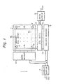
- Figure 1 illustrates a static semiconductor memory device.
- the memory device of Fig. 1 comprises a memory cell array 1 including a large number of static memory cells 2 arranged in a matrix fashion, a word decoder 3 for selecting one word line WL, an input--output gate 4 coupled to bit lines BL, a column decoder 5 for supplying the input-output gate 4 with a bit line selecting signal through the column lines CL, a data buffer 6 for outputting the data read out from the input-output gate 4 onto the data bus DB to the outside, and an address buffer 7 for receiving an input address signal ADD supplied from the outside and for supplying an inner address signal A and its inverted signal A to the word decoder 3 and the column decoder 5.
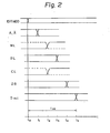
- FIG. 2 A time chart of the normal operation of the memory device of Fig. 1 is given in Fig. 2. Assume that the address signal ADD is changed at the time t 0 . The inner address signal A (A) is then changed at the time t 1 , and the reading (accessing) operation for the new address is started. The word line WL and the column line CL corresponding to the new address are selected at the time t 2 . The new data from the cell selected by the new word line is output on a bit line BL at the time t 3 , and the data corresponding to the new address is output on the data bus DB at the time t4 . The output Dout of the data buffer 6 is changed to the data corresponding to the new address at the time t 5 . Thus, the access time for reading of this memory device is t AA .
- the output data may be influenced by transient noise applied to the address signal.
- a time chart of an erroneous operation due to transient noise in the memory device of Fig. 1 is given in Fig. 3.
- the input address signal ADD is normally changed at the times t 0 and t 0 ' (after t 110 ). Before t 0 ', however, it is transiently changed by error by noise between, for example, the times t 60 and t 61 .
- the inner address signal A ( A ) is changed erroneously between the times t 70 and t 71 , the word line WL and the column line CL corresponding to the erroneous address are selected erroneously between the times t 80 and t 81 , the erroneous data from the cell corresponding to the erroneous address is output on a bit line BL between the times t 90 and t 91 , the data from the memory cell corresponding to the erroneous address is read out onto the data bus DB between the times t 100 and t 101 , and the erroneous output data Dout is output from the data buffer between the times t 110 and t 111' That is, the output data D out is changed erroneously at the time t 110 , which is later than the time t 60 by the above-mentioned access time t AA . The output data D out returns to normal at the time T 111 . Accordingly, in the illustrated semiconductor memory device of
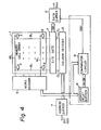
- FIG. 4 is a block diagram of this semiconductor memory device.
- the memory device of Fig. 4 further comprises an address delay buffer 8 and a comparator circuit 9.
- the address delay buffer 8 produces address signals A d, (Ad) which are delayed by a predetermined time to form the inner address signals A (A).
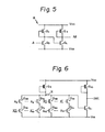
- An example of the circuit structure of the address delay buffer 8 is illustrated in Fig. 5.
- transistors Q 1 and Q 2 form a first stage inverter
- transistors Q 3 and Q 4 form a second stage-inverter.
- the transistors Q 1 and Q 3 depletion-type field-effect transistors (FET's).
- the inner address signal A is delayed by these two stage inverters to output a delayed address signal Ad.
- the inverted inner address signal A is delayed by the same circuit to obtain a delayed inverted address signal Ad.
- the number of stage, of inverters may be increased in accordance with the required delay time t D .
- the comparator circuit 9 of Fig. 4 compares the inner address signals A, ( A ) with the delayed address signal Ad, (Ad) to produce a data buffer control signal DBC for making the data buffer 6 operable only when the inner address signal A (A) and the delayed address signals Ad, (Ad) are equal to each other.
- An example of the structure of the comparator circuit 9 is illustrated in Fig. 6.
- the circuit of Fig. 6 comprises transistors Q 5 through Q 11 .
- the transistors Q 5 and Q 10 are depletion-type FET's.
- the transistor pairs Q60 and Q 70 ' Q 6n and Q 7n ' Q 80 and Q 90 , and Q 8n and Q 9n are each connected in series between the source of the transistor Q 5 and the ground V SS .
- the bits A 0 , ---, An of the inner address signal A are applied to the gates of the transistors Q 60 , --- Q 6n ; the bits Ad 0 , --- Ad n of the delayed inverted address signal Ad to the gates of the transistors Q 70 , --- Q 7n ; the bits A 0 , --- An of the inverted address A to the gates of the transistors Q 80 , --- Q 8n ; and the bits Ad 0 , --- Ad n of the delayed address A d to the gates of the transistors Q 90 , --- Q 9n .
- FIG. 7 An example of the structure of the data buffer 6 in Fig. 4, which is controlled by the control signal DBC, is illustrated in Fig. 7.
- transistors Q21 and Q 22 form a first-stage inverter INV 1 .
- the transistors Q 24 and Q 25 form a second stage inverter INV 2 which inverts the output of the first-stage inverter INV 1 .
- the transistor Q 23 is connected in parallel with the transistor Q 22
- a transistor Q 26 is connected in parallel with the transistor Q 25 .
- the control signal DBC is applied to the gates of the transistors Q 23 and Q 26 . When the control signal DBC is "H", the data reading operation of the data buffer 6 is inhibited.
- the transistors Q 27 through Q 32 form a flip-flop circuit FF.
- the outputs of the inverters INV 1 and INV 2 set or reset the flip-flop circuit FF in accordance with the level of the data on the data bus DB.
- the reading operation of the data buffer 6 is inhibited when erroneous data due to noise is output from the input-output gate circuit 5 on the data bus DB, so that this erroneous data does not appear in the output data D out .
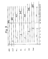
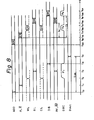
- Figure 8 is a time chart of the reading operation of the memory device of Fig. 4.
- the external address signal ADD is changed at the time t0 and is disturbed by noise between the times t 60 and t 61 , as in Fig. 3.
- the changes in the inner address signal A ( A ), the selection of the word line WL, the column line CL, and the bit line BL, and the data bus output DB are the same as those in Fig. 3.
- the delayed address signal Ad (Ad) corresponding to the inner address signal A (A) changed at the time t 1 are produced by the address delay buffer 8 at a time later than the time t 1 by the delay time t D .
- the data buffer control signal DBC from the comparator circuit 9 becomes the "H" level in the periods P 1 , P 2 , and P 3 .
- the delay time t D is adjusted in the address delay buffer 8 so that the third period P 3 coincides with the period between the times t 100 and t 101 in which the erroneous data resulting from the noise is output from the input-output gate circuit 4 onto the data bus DB. This adjustment of the delay time t D is determined by considering the delay from the change of the address to the change of the output, data, the operation delay in the comparator circuit 9, etc...
- the erroneous data Since the reading operation of the data buffer 6 is inhibited in the period in which the erroneous data resulting from the noise is output on the data bus DB, as described above, the erroneous data is-not read into the data buffer 6, and the data buffer 6 continues to output the normal data in the corresponding period.
- the data buffer control signal DBC becomes the "H" level in the periods P 1 and P 2 besides the period P 3 , it does not influence the reading operation of the memory device of Fig. 4, as described below.
- the period P 1 is finished at the time t 4 and as the data corresponding to the address changes at the time t 0 is output onto the data bus at the time t 4 , this data is read into the data buffer 6, and the output data D out is changed at time t 5 .
- the access time for reading in the memory device of Fig. 4 is t AA , just as in the memory device of Fig. 1.
- the data buffer 6 continues to output normal data.
- a memory device embodying the present invention may be formed on a single or a plurality of semiconductor substrates.
Landscapes
- Engineering & Computer Science (AREA)
- Computer Security & Cryptography (AREA)
- Microelectronics & Electronic Packaging (AREA)
- Static Random-Access Memory (AREA)
- Techniques For Improving Reliability Of Storages (AREA)
- Semiconductor Memories (AREA)
- For Increasing The Reliability Of Semiconductor Memories (AREA)
Applications Claiming Priority (2)
| Application Number | Priority Date | Filing Date | Title |
|---|---|---|---|
| JP57161694A JPS5952492A (ja) | 1982-09-17 | 1982-09-17 | スタテイツク型半導体記憶装置 |
| JP161694/82 | 1982-09-17 |
Publications (3)
| Publication Number | Publication Date |
|---|---|
| EP0104850A2 true EP0104850A2 (de) | 1984-04-04 |
| EP0104850A3 EP0104850A3 (en) | 1987-03-11 |
| EP0104850B1 EP0104850B1 (de) | 1990-07-11 |
Family
ID=15740081
Family Applications (1)
| Application Number | Title | Priority Date | Filing Date |
|---|---|---|---|
| EP19830305462 Expired EP0104850B1 (de) | 1982-09-17 | 1983-09-16 | Halbleiterspeicheranordnung |
Country Status (4)
| Country | Link |
|---|---|
| US (1) | US4982366A (de) |
| EP (1) | EP0104850B1 (de) |
| JP (1) | JPS5952492A (de) |
| DE (1) | DE3381723D1 (de) |
Cited By (4)
| Publication number | Priority date | Publication date | Assignee | Title |
|---|---|---|---|---|
| US4766572A (en) * | 1984-12-27 | 1988-08-23 | Nec Corporation | Semiconductor memory having a bypassable data output latch |
| EP0386831A1 (de) * | 1989-03-07 | 1990-09-12 | Digital Equipment Corporation | Vergleichsschaltung mit einem Maskiermechanismus zum Maskieren von Übergangsdifferenzen, Vergleichsschaltungssystem und Verarbeitungseinrichtung mit einer solchen Vergleichsschaltung |
| EP0476160A1 (de) * | 1989-07-15 | 1992-03-25 | Bodenseewerk Gerätetechnik GmbH | Einrichtung zur Erzeugung von Messsignalen mit einer Mehrzahl von redundant vorgesehenen Sensoren |
| GB2342739A (en) * | 1998-07-17 | 2000-04-19 | Sun Microsystems Inc | Memory address checking within a solid state memory device |
Families Citing this family (10)
| Publication number | Priority date | Publication date | Assignee | Title |
|---|---|---|---|---|
| JPS63163548A (ja) * | 1986-12-24 | 1988-07-07 | Mitsubishi Electric Corp | メモリアクセス回路 |
| US5228003A (en) * | 1988-04-15 | 1993-07-13 | Seiko Epson Corporation | Semiconductor memory |
| JPH0253111U (de) * | 1988-10-11 | 1990-04-17 | ||
| US5379212A (en) * | 1990-01-29 | 1995-01-03 | United States Voting Machines, Inc. | Locking memory device |
| JPH04259997A (ja) * | 1991-02-15 | 1992-09-16 | Nec Ic Microcomput Syst Ltd | 半導体集積回路 |
| JP2719852B2 (ja) * | 1991-03-07 | 1998-02-25 | 三菱電機株式会社 | 半導体記憶装置およびそれからのデータ読出方法 |
| IT1253678B (it) * | 1991-07-31 | 1995-08-22 | St Microelectronics Srl | Architettura antirumore per memoria |
| JPH05250872A (ja) * | 1992-03-09 | 1993-09-28 | Oki Electric Ind Co Ltd | ランダム・アクセス・メモリ |
| US5272674A (en) * | 1992-09-21 | 1993-12-21 | Atmel Corporation | High speed memory sense amplifier with noise reduction |
| US9011003B2 (en) * | 2006-02-08 | 2015-04-21 | S.C. Johnson Home Storage, Inc. | Reclosable pouch and zipper for a reclosable pouch |
Citations (3)
| Publication number | Priority date | Publication date | Assignee | Title |
|---|---|---|---|---|
| US3036272A (en) * | 1957-06-27 | 1962-05-22 | Rca Corp | Pulse width discriminator |
| GB2027958A (en) * | 1978-08-04 | 1980-02-27 | Honeywell Inf Systems | Microprogrammed control unit |
| US4337525A (en) * | 1979-04-17 | 1982-06-29 | Nippon Electric Co., Ltd. | Asynchronous circuit responsive to changes in logic level |
Family Cites Families (6)
| Publication number | Priority date | Publication date | Assignee | Title |
|---|---|---|---|---|
| JPS6057156B2 (ja) * | 1978-05-24 | 1985-12-13 | 株式会社日立製作所 | 半導体メモリ装置 |
| JPS5668030A (en) * | 1979-11-07 | 1981-06-08 | Nec Corp | Logic circuit |
| JPS578988A (en) * | 1980-06-18 | 1982-01-18 | Toshiba Corp | Semiconductor memory |
| JPS5835783A (ja) * | 1981-08-24 | 1983-03-02 | Fujitsu Ltd | 半導体メモリ |
| US4486883A (en) * | 1982-02-03 | 1984-12-04 | Clarion Co., Ltd. | Address check system |
| JPS58169383A (ja) * | 1982-03-30 | 1983-10-05 | Fujitsu Ltd | 半導体記憶装置 |
-
1982
- 1982-09-17 JP JP57161694A patent/JPS5952492A/ja active Granted
-
1983
- 1983-09-16 EP EP19830305462 patent/EP0104850B1/de not_active Expired
- 1983-09-16 DE DE8383305462T patent/DE3381723D1/de not_active Expired - Lifetime
-
1990
- 1990-01-22 US US07/467,348 patent/US4982366A/en not_active Expired - Lifetime
Patent Citations (3)
| Publication number | Priority date | Publication date | Assignee | Title |
|---|---|---|---|---|
| US3036272A (en) * | 1957-06-27 | 1962-05-22 | Rca Corp | Pulse width discriminator |
| GB2027958A (en) * | 1978-08-04 | 1980-02-27 | Honeywell Inf Systems | Microprogrammed control unit |
| US4337525A (en) * | 1979-04-17 | 1982-06-29 | Nippon Electric Co., Ltd. | Asynchronous circuit responsive to changes in logic level |
Cited By (5)
| Publication number | Priority date | Publication date | Assignee | Title |
|---|---|---|---|---|
| US4766572A (en) * | 1984-12-27 | 1988-08-23 | Nec Corporation | Semiconductor memory having a bypassable data output latch |
| EP0386831A1 (de) * | 1989-03-07 | 1990-09-12 | Digital Equipment Corporation | Vergleichsschaltung mit einem Maskiermechanismus zum Maskieren von Übergangsdifferenzen, Vergleichsschaltungssystem und Verarbeitungseinrichtung mit einer solchen Vergleichsschaltung |
| EP0476160A1 (de) * | 1989-07-15 | 1992-03-25 | Bodenseewerk Gerätetechnik GmbH | Einrichtung zur Erzeugung von Messsignalen mit einer Mehrzahl von redundant vorgesehenen Sensoren |
| GB2342739A (en) * | 1998-07-17 | 2000-04-19 | Sun Microsystems Inc | Memory address checking within a solid state memory device |
| GB2342739B (en) * | 1998-07-17 | 2001-07-11 | Sun Microsystems Inc | Memory address checking |
Also Published As
| Publication number | Publication date |
|---|---|
| EP0104850A3 (en) | 1987-03-11 |
| EP0104850B1 (de) | 1990-07-11 |
| JPS6346920B2 (de) | 1988-09-19 |
| DE3381723D1 (de) | 1990-08-16 |
| US4982366A (en) | 1991-01-01 |
| JPS5952492A (ja) | 1984-03-27 |
Similar Documents
| Publication | Publication Date | Title |
|---|---|---|
| EP0090590B1 (de) | Halbleiter-Speichervorrichtung | |
| US4953128A (en) | Variable delay circuit for delaying input data | |
| US4575819A (en) | Memory with RAM cells and ROM cells | |
| EP0143647B1 (de) | Halbleiterspeicheranordnung | |
| US5546355A (en) | Integrated circuit memory having a self-timed write pulse independent of clock frequency and duty cycle | |
| EP0104850A2 (de) | Halbleiterspeicheranordnung | |
| JPS5942396B2 (ja) | 半導体メモリ装置 | |
| US5436865A (en) | Output circuit for semiconductor memory device realizing extended data output upon inactivation of CAS signal | |
| EP0311047B1 (de) | Dynamischer RAM-Speicher | |
| JPS5951073B2 (ja) | 半導体記憶装置 | |
| US5889727A (en) | Circuit for reducing the transmission delay of the redundancy evaluation for synchronous DRAM | |
| US5886553A (en) | Semiconductor device having a latch circuit for latching data externally input | |
| KR910004733B1 (ko) | 데이타 버스 리셋트 회로를 지닌 반도체 기억장치 | |
| EP0793235B1 (de) | Einchipspeichersystem mit einem Dekoder für Pulswortleitungsverfahren | |
| JP2960752B2 (ja) | 半導体記憶装置 | |
| KR950012025B1 (ko) | 상이타이밍에 인가되는 2개 전원전압을 동시에 공급하는 타이밍일치회로 | |
| US5034924A (en) | Static random access memory device with pull-down control circuit | |
| EP0262850A2 (de) | Speicherzellschaltung | |
| US5499210A (en) | Low power consumption semiconductor memory | |
| JPH0263280B2 (de) | ||
| JP2804212B2 (ja) | 半導体記憶装置 | |
| EP0475448B1 (de) | Halbleiterspeicheranordnung mit einem Absenktransistor für externes Signal | |
| JPH05101651A (ja) | ダイナミツク型半導体記憶装置 | |
| KR960009947B1 (ko) | 디램의 리프레쉬 회로 | |
| JP2506420B2 (ja) | 半導体記憶装置 |
Legal Events
| Date | Code | Title | Description |
|---|---|---|---|
| PUAI | Public reference made under article 153(3) epc to a published international application that has entered the european phase |
Free format text: ORIGINAL CODE: 0009012 |
|
| AK | Designated contracting states |
Designated state(s): DE FR GB |
|
| PUAL | Search report despatched |
Free format text: ORIGINAL CODE: 0009013 |
|
| AK | Designated contracting states |
Kind code of ref document: A3 Designated state(s): DE FR GB |
|
| 17P | Request for examination filed |
Effective date: 19870602 |
|
| 17Q | First examination report despatched |
Effective date: 19880215 |
|
| GRAA | (expected) grant |
Free format text: ORIGINAL CODE: 0009210 |
|
| AK | Designated contracting states |
Kind code of ref document: B1 Designated state(s): DE FR GB |
|
| ET | Fr: translation filed | ||
| REF | Corresponds to: |
Ref document number: 3381723 Country of ref document: DE Date of ref document: 19900816 |
|
| RIN2 | Information on inventor provided after grant (corrected) |
Free format text: TAKEMAE, YOSHIHIRO SHUWA-AKASAKAHINOKICHO |
|
| PLBE | No opposition filed within time limit |
Free format text: ORIGINAL CODE: 0009261 |
|
| STAA | Information on the status of an ep patent application or granted ep patent |
Free format text: STATUS: NO OPPOSITION FILED WITHIN TIME LIMIT |
|
| 26N | No opposition filed | ||
| REG | Reference to a national code |
Ref country code: GB Ref legal event code: IF02 |
|
| PGFP | Annual fee paid to national office [announced via postgrant information from national office to epo] |
Ref country code: FR Payment date: 20020910 Year of fee payment: 20 |
|
| PGFP | Annual fee paid to national office [announced via postgrant information from national office to epo] |
Ref country code: GB Payment date: 20020911 Year of fee payment: 20 |
|
| PGFP | Annual fee paid to national office [announced via postgrant information from national office to epo] |
Ref country code: DE Payment date: 20020925 Year of fee payment: 20 |
|
| PG25 | Lapsed in a contracting state [announced via postgrant information from national office to epo] |
Ref country code: GB Free format text: LAPSE BECAUSE OF EXPIRATION OF PROTECTION Effective date: 20030915 |
|
| REG | Reference to a national code |
Ref country code: GB Ref legal event code: PE20 |