EP0103523B1 - Herstellungsverfahren eines Dünnschichttransistoren und Kondensatoren enthaltenden Bildschirmes - Google Patents
Herstellungsverfahren eines Dünnschichttransistoren und Kondensatoren enthaltenden Bildschirmes Download PDFInfo
- Publication number
- EP0103523B1 EP0103523B1 EP83401775A EP83401775A EP0103523B1 EP 0103523 B1 EP0103523 B1 EP 0103523B1 EP 83401775 A EP83401775 A EP 83401775A EP 83401775 A EP83401775 A EP 83401775A EP 0103523 B1 EP0103523 B1 EP 0103523B1
- Authority
- EP
- European Patent Office
- Prior art keywords
- layer
- deposit
- conductive material
- photoengraving
- column
- Prior art date
- Legal status (The legal status is an assumption and is not a legal conclusion. Google has not performed a legal analysis and makes no representation as to the accuracy of the status listed.)
- Expired
Links
- 238000004519 manufacturing process Methods 0.000 title claims description 12
- 239000003990 capacitor Substances 0.000 title description 10
- 239000010409 thin film Substances 0.000 title description 3
- 238000000034 method Methods 0.000 claims description 20
- XUIMIQQOPSSXEZ-UHFFFAOYSA-N Silicon Chemical compound [Si] XUIMIQQOPSSXEZ-UHFFFAOYSA-N 0.000 claims description 11
- 229910021417 amorphous silicon Inorganic materials 0.000 claims description 11
- 239000004020 conductor Substances 0.000 claims description 10
- 229910052710 silicon Inorganic materials 0.000 claims description 8
- 239000010703 silicon Substances 0.000 claims description 8
- 239000011159 matrix material Substances 0.000 claims description 5
- 239000000758 substrate Substances 0.000 claims description 5
- 238000002161 passivation Methods 0.000 claims description 4
- 239000011810 insulating material Substances 0.000 claims 1
- 238000005530 etching Methods 0.000 description 13
- VYPSYNLAJGMNEJ-UHFFFAOYSA-N Silicium dioxide Chemical compound O=[Si]=O VYPSYNLAJGMNEJ-UHFFFAOYSA-N 0.000 description 7
- 238000000151 deposition Methods 0.000 description 6
- 230000008021 deposition Effects 0.000 description 6
- 239000004973 liquid crystal related substance Substances 0.000 description 6
- 229910052782 aluminium Inorganic materials 0.000 description 4
- XAGFODPZIPBFFR-UHFFFAOYSA-N aluminium Chemical compound [Al] XAGFODPZIPBFFR-UHFFFAOYSA-N 0.000 description 4
- 239000011521 glass Substances 0.000 description 3
- 230000000873 masking effect Effects 0.000 description 3
- 239000000377 silicon dioxide Substances 0.000 description 3
- ATJFFYVFTNAWJD-UHFFFAOYSA-N Tin Chemical compound [Sn] ATJFFYVFTNAWJD-UHFFFAOYSA-N 0.000 description 2
- 210000004027 cell Anatomy 0.000 description 2
- 230000005669 field effect Effects 0.000 description 2
- 229910003437 indium oxide Inorganic materials 0.000 description 2
- PJXISJQVUVHSOJ-UHFFFAOYSA-N indium(iii) oxide Chemical compound [O-2].[O-2].[O-2].[In+3].[In+3] PJXISJQVUVHSOJ-UHFFFAOYSA-N 0.000 description 2
- 238000009413 insulation Methods 0.000 description 2
- 238000001465 metallisation Methods 0.000 description 2
- 239000004065 semiconductor Substances 0.000 description 2
- 229910001887 tin oxide Inorganic materials 0.000 description 2
- VYZAMTAEIAYCRO-UHFFFAOYSA-N Chromium Chemical compound [Cr] VYZAMTAEIAYCRO-UHFFFAOYSA-N 0.000 description 1
- 241001415961 Gaviidae Species 0.000 description 1
- 229910052581 Si3N4 Inorganic materials 0.000 description 1
- 241001639412 Verres Species 0.000 description 1
- 238000009825 accumulation Methods 0.000 description 1
- 239000004411 aluminium Substances 0.000 description 1
- 229910052804 chromium Inorganic materials 0.000 description 1
- 239000011651 chromium Substances 0.000 description 1
- 238000004140 cleaning Methods 0.000 description 1
- 210000002858 crystal cell Anatomy 0.000 description 1
- 229910052738 indium Inorganic materials 0.000 description 1
- APFVFJFRJDLVQX-UHFFFAOYSA-N indium atom Chemical compound [In] APFVFJFRJDLVQX-UHFFFAOYSA-N 0.000 description 1
- 239000012212 insulator Substances 0.000 description 1
- 230000003287 optical effect Effects 0.000 description 1
- 230000003071 parasitic effect Effects 0.000 description 1
- 238000002360 preparation method Methods 0.000 description 1
- 230000002787 reinforcement Effects 0.000 description 1
- HQVNEWCFYHHQES-UHFFFAOYSA-N silicon nitride Chemical compound N12[Si]34N5[Si]62N3[Si]51N64 HQVNEWCFYHHQES-UHFFFAOYSA-N 0.000 description 1
Images


Classifications
-
- G—PHYSICS
- G02—OPTICS
- G02F—OPTICAL DEVICES OR ARRANGEMENTS FOR THE CONTROL OF LIGHT BY MODIFICATION OF THE OPTICAL PROPERTIES OF THE MEDIA OF THE ELEMENTS INVOLVED THEREIN; NON-LINEAR OPTICS; FREQUENCY-CHANGING OF LIGHT; OPTICAL LOGIC ELEMENTS; OPTICAL ANALOGUE/DIGITAL CONVERTERS
- G02F1/00—Devices or arrangements for the control of the intensity, colour, phase, polarisation or direction of light arriving from an independent light source, e.g. switching, gating or modulating; Non-linear optics
- G02F1/01—Devices or arrangements for the control of the intensity, colour, phase, polarisation or direction of light arriving from an independent light source, e.g. switching, gating or modulating; Non-linear optics for the control of the intensity, phase, polarisation or colour
- G02F1/13—Devices or arrangements for the control of the intensity, colour, phase, polarisation or direction of light arriving from an independent light source, e.g. switching, gating or modulating; Non-linear optics for the control of the intensity, phase, polarisation or colour based on liquid crystals, e.g. single liquid crystal display cells
- G02F1/133—Constructional arrangements; Operation of liquid crystal cells; Circuit arrangements
- G02F1/136—Liquid crystal cells structurally associated with a semi-conducting layer or substrate, e.g. cells forming part of an integrated circuit
- G02F1/1362—Active matrix addressed cells
- G02F1/1368—Active matrix addressed cells in which the switching element is a three-electrode device
-
- H—ELECTRICITY
- H10—SEMICONDUCTOR DEVICES; ELECTRIC SOLID-STATE DEVICES NOT OTHERWISE PROVIDED FOR
- H10D—INORGANIC ELECTRIC SEMICONDUCTOR DEVICES
- H10D30/00—Field-effect transistors [FET]
- H10D30/60—Insulated-gate field-effect transistors [IGFET]
- H10D30/67—Thin-film transistors [TFT]
- H10D30/6729—Thin-film transistors [TFT] characterised by the electrodes
- H10D30/673—Thin-film transistors [TFT] characterised by the electrodes characterised by the shapes, relative sizes or dispositions of the gate electrodes
- H10D30/6731—Top-gate only TFTs
-
- H—ELECTRICITY
- H10—SEMICONDUCTOR DEVICES; ELECTRIC SOLID-STATE DEVICES NOT OTHERWISE PROVIDED FOR
- H10D—INORGANIC ELECTRIC SEMICONDUCTOR DEVICES
- H10D30/00—Field-effect transistors [FET]
- H10D30/60—Insulated-gate field-effect transistors [IGFET]
- H10D30/67—Thin-film transistors [TFT]
- H10D30/674—Thin-film transistors [TFT] characterised by the active materials
- H10D30/6741—Group IV materials, e.g. germanium or silicon carbide
- H10D30/6743—Silicon
- H10D30/6746—Amorphous silicon
-
- H—ELECTRICITY
- H10—SEMICONDUCTOR DEVICES; ELECTRIC SOLID-STATE DEVICES NOT OTHERWISE PROVIDED FOR
- H10D—INORGANIC ELECTRIC SEMICONDUCTOR DEVICES
- H10D86/00—Integrated devices formed in or on insulating or conducting substrates, e.g. formed in silicon-on-insulator [SOI] substrates or on stainless steel or glass substrates
- H10D86/40—Integrated devices formed in or on insulating or conducting substrates, e.g. formed in silicon-on-insulator [SOI] substrates or on stainless steel or glass substrates characterised by multiple TFTs
-
- H—ELECTRICITY
- H10—SEMICONDUCTOR DEVICES; ELECTRIC SOLID-STATE DEVICES NOT OTHERWISE PROVIDED FOR
- H10D—INORGANIC ELECTRIC SEMICONDUCTOR DEVICES
- H10D86/00—Integrated devices formed in or on insulating or conducting substrates, e.g. formed in silicon-on-insulator [SOI] substrates or on stainless steel or glass substrates
- H10D86/40—Integrated devices formed in or on insulating or conducting substrates, e.g. formed in silicon-on-insulator [SOI] substrates or on stainless steel or glass substrates characterised by multiple TFTs
- H10D86/441—Interconnections, e.g. scanning lines
-
- H—ELECTRICITY
- H10—SEMICONDUCTOR DEVICES; ELECTRIC SOLID-STATE DEVICES NOT OTHERWISE PROVIDED FOR
- H10D—INORGANIC ELECTRIC SEMICONDUCTOR DEVICES
- H10D86/00—Integrated devices formed in or on insulating or conducting substrates, e.g. formed in silicon-on-insulator [SOI] substrates or on stainless steel or glass substrates
- H10D86/40—Integrated devices formed in or on insulating or conducting substrates, e.g. formed in silicon-on-insulator [SOI] substrates or on stainless steel or glass substrates characterised by multiple TFTs
- H10D86/60—Integrated devices formed in or on insulating or conducting substrates, e.g. formed in silicon-on-insulator [SOI] substrates or on stainless steel or glass substrates characterised by multiple TFTs wherein the TFTs are in active matrices
-
- H—ELECTRICITY
- H10—SEMICONDUCTOR DEVICES; ELECTRIC SOLID-STATE DEVICES NOT OTHERWISE PROVIDED FOR
- H10D—INORGANIC ELECTRIC SEMICONDUCTOR DEVICES
- H10D86/00—Integrated devices formed in or on insulating or conducting substrates, e.g. formed in silicon-on-insulator [SOI] substrates or on stainless steel or glass substrates
- H10D86/80—Integrated devices formed in or on insulating or conducting substrates, e.g. formed in silicon-on-insulator [SOI] substrates or on stainless steel or glass substrates characterised by multiple passive components, e.g. resistors, capacitors or inductors
-
- G—PHYSICS
- G02—OPTICS
- G02F—OPTICAL DEVICES OR ARRANGEMENTS FOR THE CONTROL OF LIGHT BY MODIFICATION OF THE OPTICAL PROPERTIES OF THE MEDIA OF THE ELEMENTS INVOLVED THEREIN; NON-LINEAR OPTICS; FREQUENCY-CHANGING OF LIGHT; OPTICAL LOGIC ELEMENTS; OPTICAL ANALOGUE/DIGITAL CONVERTERS
- G02F2202/00—Materials and properties
- G02F2202/10—Materials and properties semiconductor
- G02F2202/103—Materials and properties semiconductor a-Si
Definitions
- the present invention relates to a method of manufacturing an active matrix display screen, based on thin film transistors and capacitors. It finds an application in particular in the production of liquid crystal display circuits.
- Thin film transistor circuits are mainly used in the manufacture of active matrix display screens.
- an electronic memory formed by memory points distributed over the entire surface of the screen stores the video signal throughout the duration of the image.
- the electrooptical transducer for example a liquid crystal
- the electrooptical transducer is in contact with each memory point, and is excited for the entire duration of an image, whereas, in systems without electronic memory, the transducer is only excited for the duration of a line.
- the optical effect and the authorized multiplexing rate are therefore much greater.
- the TCM makes it possible to produce such an electronic memory on a glass substrate.
- Each memory point is located at the intersection of a line and a connection column - and it consists of a transistor and a capacitor.
- the transducer is a liquid crystal
- the plates of the capacitor can be formed by the electrodes of the liquid crystal cell itself.
- the memory point is therefore reduced to a TCM and to a capacitor, one of the armatures of which is constituted by the electrode placed on the wall of the cell which contains the TCM, the other armature being constituted by the counter-electrode arranged on the other wall of the cell.
- FIG. 1 Such a structure is shown in FIG. 1. There is seen, on the one hand, a lower wall 10 carrying conductive columns 12 and conductive lines 14, a TCM 20 and a transparent electrode 22, and on the other hand, a upper wall 24 covered with a counter-electrode 26 also transparent.
- circuits can be produced with TCMs and, for example, all or part of shift registers. Such circuits can be used in the low rate vertical register, which allows line to line switching of the display screen.
- FIG. 2 (a, b) illustrates a technique described by AJ SNELL et al in an article entitled “Application of Amorphous Silicon Field Effect Transistors in Adressable Liquid Crystal Display Panels” published in "Applied Physics” 24, 357-362 (1981) .
- the TCM is formed by a grid G in chromium deposited on an insulating substrate 30, an insulating layer 32 made of silicon nitride (Si 3 N 4 ), a layer of amorphous silicon 34 (a Si), a drain D and a source S of aluminum.
- the lower reinforcement of the capacitor is formed of a layer 38 of tin and indium oxide.
- connection between the TCM and the armature is made by the drain D extended by a lug 40 which borrows a contact hole 42 made in the insulating layer 32.
- the entire circuit consists of a plurality of such structures arranged in matrix form.
- the grids G are formed by connection lines 44 and the sources by columns 46.
- Such a method has two drawbacks: firstly, it requires numerous masks; then. it requires that the etching of the sources and the drains is selective and non-polluting with respect to the amorphous silicon, which must be protected by an adequate passivation which must not create a zone of accumulation at the upper interface.
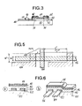
- TCM manufacturing technique in which, unlike the previous one, the TCM has its source and drain contacts at the bottom and its grid at the top. This technique is described by M. Matsumura et al in the article entitled “Amorphous Silicon Integrated Circuit published in” Proceedings of the IEE ", vol 68, n ° 10, October 1980, pages 1349-1350. It is illustrated by FIG. 3.
- a layer 52 of amorphous silicon On a glass support 50 is deposited a layer 52 of amorphous silicon, then a layer of n + doped silicon, which is then etched to form the source 54 and drain 56 contacts; an insulating layer 58 of silica is deposited on the assembly; openings 60, 62 are made in this insulating layer to give access to the source and to the drain; an aluminum layer forms the grid 64.
- the frame of the capacitor is formed by a layer 66 of transparent conductive oxide, covered by the layer 58 of silica; an opening 68 is made in this layer and a connection 70 connects the source 54 to the electrode 66.
- the present invention aims to avoid these drawbacks by reducing the number of masking levels from 5 (or 6) to 2. Thanks to the invention, better manufacturing yields are therefore obtained and the production rate of the circuits is increased.
- the process of the present invention does not necessarily suppose that the silicon is deposited by CVD-plasma at high temperature, and other techniques are possible, in particular those which operate at lower temperature (250 ° C-300 ° C ).
- FIG. 5 shows, in an enlarged manner, the constitution of the TCMs in the zone of overlap of a line 116 and of a column 104.
- the source and the drain are respectively constituted by the appendix 108 and the part of the column 104 located under line 116; the control gate is formed by the part of line 116 which is located between appendix 108 and column 104.
- TCM parasitic transistor
- the second mask can be placed, relative to the first, with a margin of error which allows the implementation of an automatic alignment. This faculty further simplifies the method of the invention.
- the oxide 102 If it is desired to improve the contact between the oxide 102 and the layer 110 of aSiH, it is possible to deposit, after the oxide, a layer of highly n-doped amorphous silicon (by adding for example PH 3 in SiH 4 ) to the time of filing. This is what is illustrated in FIG. 6 where this layer bears the reference 120.
- the etching of the first level is carried out using the same mask and this etching then affects the doped silicon layer 120 and that of the oxide 102.
- the other operations are identical.
- the doped silicon is attacked following the semiconductor silicon. The doped silicon therefore only remains under the gate, above the oxide (FIG. 6b).
Landscapes
- Physics & Mathematics (AREA)
- Nonlinear Science (AREA)
- Mathematical Physics (AREA)
- Engineering & Computer Science (AREA)
- Chemical & Material Sciences (AREA)
- Crystallography & Structural Chemistry (AREA)
- Microelectronics & Electronic Packaging (AREA)
- General Physics & Mathematics (AREA)
- Optics & Photonics (AREA)
- Liquid Crystal (AREA)
- Thin Film Transistor (AREA)
- Semiconductor Integrated Circuits (AREA)
- Devices For Indicating Variable Information By Combining Individual Elements (AREA)
Claims (2)
Applications Claiming Priority (2)
| Application Number | Priority Date | Filing Date | Title |
|---|---|---|---|
| FR8215499 | 1982-09-14 | ||
| FR8215499A FR2533072B1 (fr) | 1982-09-14 | 1982-09-14 | Procede de fabrication de circuits electroniques a base de transistors en couches minces et de condensateurs |
Publications (2)
| Publication Number | Publication Date |
|---|---|
| EP0103523A1 EP0103523A1 (de) | 1984-03-21 |
| EP0103523B1 true EP0103523B1 (de) | 1987-05-27 |
Family
ID=9277431
Family Applications (1)
| Application Number | Title | Priority Date | Filing Date |
|---|---|---|---|
| EP83401775A Expired EP0103523B1 (de) | 1982-09-14 | 1983-09-12 | Herstellungsverfahren eines Dünnschichttransistoren und Kondensatoren enthaltenden Bildschirmes |
Country Status (7)
| Country | Link |
|---|---|
| US (1) | US4563806A (de) |
| EP (1) | EP0103523B1 (de) |
| JP (1) | JPS59501562A (de) |
| CA (1) | CA1224262A (de) |
| DE (1) | DE3371838D1 (de) |
| FR (1) | FR2533072B1 (de) |
| WO (1) | WO1984001239A1 (de) |
Families Citing this family (35)
| Publication number | Priority date | Publication date | Assignee | Title |
|---|---|---|---|---|
| US5123847A (en) * | 1983-05-11 | 1992-06-23 | Holmberg Scott H | Method of manufacturing flat panel backplanes, display transistors |
| FR2571913B1 (fr) * | 1984-10-17 | 1986-12-26 | Richard Joseph | Ecran d'affichage a matrice active a double transistor d'adressage |
| JPH0627980B2 (ja) * | 1984-10-17 | 1994-04-13 | レタ・フランセ・ルプレザント・パ・ル・ミニストル・デ・ペ・テ・テ・(セントル・ナシヨナル・デチユ−ド・デ・テレコミユニカシオン) | 能動マトリクスデイスプレイスクリ−ンの製造方法 |
| JPS61138285A (ja) * | 1984-12-10 | 1986-06-25 | ホシデン株式会社 | 液晶表示素子 |
| FR2579806B1 (fr) * | 1985-03-26 | 1987-05-07 | Morin Francois | Procede de fabrication d'un ecran d'affichage a cristaux liquides et a reseau de diodes |
| JPH0740101B2 (ja) * | 1985-04-23 | 1995-05-01 | 旭硝子株式会社 | 薄膜トランジスタ |
| FR2586859B1 (fr) * | 1985-08-27 | 1987-11-20 | Thomson Csf | Procede de fabrication d'un transistor de commande pour ecran plat de visualisation et element de commande realise selon ce procede |
| JPS61160428U (de) * | 1985-10-28 | 1986-10-04 | ||
| FR2590406B1 (fr) * | 1985-11-15 | 1988-10-28 | Commissariat Energie Atomique | Procede de fabrication d'un transistor en couches minces a grille auto-alignee par rapport au drain et a la source de celui-ci |
| FR2593327B1 (fr) * | 1986-01-23 | 1988-10-28 | Commissariat Energie Atomique | Procede de fabrication d'un transistor en couches minces utilisant deux ou trois niveaux de masquage |
| FR2593629B1 (fr) * | 1986-01-27 | 1988-03-18 | Maurice Francois | Ecran d'affichage a matrice active et a redondance lignes et colonnes |
| FR2602361B1 (fr) * | 1986-01-27 | 1989-05-19 | Maurice Francois | Ecran d'affichage a matrice active sans transistor parasite et procede de fabrication de cet ecran |
| FR2593631B1 (fr) * | 1986-01-27 | 1989-02-17 | Maurice Francois | Ecran d'affichage a matrice active a resistance de grille et procedes de fabrication de cet ecran |
| FR2593630B1 (fr) * | 1986-01-27 | 1988-03-18 | Maurice Francois | Ecran d'affichage a matrice active a resistance de drain et procedes de fabrication de cet ecran |
| FR2593632B1 (fr) * | 1986-01-27 | 1988-03-18 | Maurice Francois | Ecran d'affichage a matrice active et procedes de realisation de cet ecran |
| US4704783A (en) * | 1986-05-05 | 1987-11-10 | General Electric Company | Method for passivating the back channel of amorphous silicon field effect transistors |
| FR2601801B1 (fr) * | 1986-07-16 | 1988-09-16 | Morin Francois | Ecran d'affichage a matrice active utilisant du carbure de silicium amorphe hydrogene et procede de fabrication de cet ecran |
| FR2605442B1 (fr) * | 1986-10-17 | 1988-12-09 | Thomson Csf | Ecran de visualisation electrooptique a transistors de commande et procede de realisation |
| FR2605438B1 (fr) * | 1986-10-17 | 1989-12-15 | Maurice Francois | Ecran d'affichage a cristaux liquides concu pour eliminer les defauts dus aux espaceurs |
| US4803536A (en) * | 1986-10-24 | 1989-02-07 | Xerox Corporation | Electrostatic discharge protection network for large area transducer arrays |
| JP2501118B2 (ja) * | 1988-06-17 | 1996-05-29 | 忠弘 大見 | 半導体装置の製造方法 |
| FR2640809B1 (fr) * | 1988-12-19 | 1993-10-22 | Chouan Yannick | Procede de gravure d'une couche d'oxyde metallique et depot simultane d'un film de polymere, application de ce procede a la fabrication d'un transistor |
| US5148333A (en) * | 1988-12-21 | 1992-09-15 | Sony Corp. | Method for recording and/or reproducing a signal |
| EP0376329B1 (de) * | 1988-12-28 | 1995-03-08 | Sony Corporation | Flüssigkristall-Anzeigevorrichtung |
| US4968119A (en) * | 1989-01-10 | 1990-11-06 | David Sarnoff Research Center, Inc. | High-density liquid-crystal active dot-matrix display structure |
| FR2662290B1 (fr) * | 1990-05-15 | 1992-07-24 | France Telecom | Procede de realisation d'un ecran d'affichage a matrice active et a condensateurs de stockage et ecran obtenu par ce procede. |
| JPH0772510A (ja) * | 1993-09-07 | 1995-03-17 | Hitachi Ltd | アクティブマトリクス型液晶表示装置 |
| US5546204A (en) * | 1994-05-26 | 1996-08-13 | Honeywell Inc. | TFT matrix liquid crystal device having data source lines and drain means of etched and doped single crystal silicon |
| FR2721428B1 (fr) | 1994-06-17 | 1996-09-13 | France Telecom | Ecran d'affichage à matrice active à commande multiplexée. |
| US5691782A (en) * | 1994-07-08 | 1997-11-25 | Sanyo Electric Co., Ltd. | Liquid-crystal display with inter-line short-circuit preventive function and process for producing same |
| TW347477B (en) * | 1994-09-30 | 1998-12-11 | Sanyo Electric Co | Liquid crystal display with storage capacitors for holding electric charges |
| US5777703A (en) * | 1994-09-30 | 1998-07-07 | Sanyo Electric Co., Ltd. | Active matrix type liquid crystal display apparatus with a projection part in the drain line |
| JP3081474B2 (ja) * | 1994-11-11 | 2000-08-28 | 三洋電機株式会社 | 液晶表示装置 |
| FR2732781B1 (fr) * | 1995-04-07 | 1997-06-20 | Thomson Lcd | Procede de fabrication de matrice active tft pour ecran de systeme de projection |
| JPH09318975A (ja) * | 1996-05-30 | 1997-12-12 | Nec Corp | 薄膜電界効果型トランジスタ素子アレイおよびその製造 方法 |
Family Cites Families (9)
| Publication number | Priority date | Publication date | Assignee | Title |
|---|---|---|---|---|
| US4024626A (en) * | 1974-12-09 | 1977-05-24 | Hughes Aircraft Company | Method of making integrated transistor matrix for flat panel liquid crystal display |
| US4188095A (en) * | 1975-07-29 | 1980-02-12 | Citizen Watch Co., Ltd. | Liquid type display cells and method of manufacturing the same |
| US4167806A (en) * | 1976-09-28 | 1979-09-18 | Commissariat A L'energie Atomique | Method of fabrication of an amorphous semiconductor device on a substrate |
| JPS54154289A (en) * | 1978-05-26 | 1979-12-05 | Matsushita Electric Ind Co Ltd | Manufacture of thin-film transistor array |
| FR2478879A1 (fr) * | 1980-03-24 | 1981-09-25 | Commissariat Energie Atomique | Procede de realisation de dispositifs a effet memoire a semi-conducteurs amorphes |
| JPS56162793A (en) * | 1980-05-19 | 1981-12-14 | Canon Kk | Display unit |
| JPS56161676A (en) * | 1980-05-16 | 1981-12-12 | Japan Electronic Ind Dev Assoc<Jeida> | Electrode structure for thin film transistor |
| US4335161A (en) * | 1980-11-03 | 1982-06-15 | Xerox Corporation | Thin film transistors, thin film transistor arrays, and a process for preparing the same |
| FR2518810A1 (fr) * | 1981-12-23 | 1983-06-24 | Morin Francois | Procede de fabrication de transistors en couches minces en silicium sur substrat isolant |
-
1982
- 1982-09-14 FR FR8215499A patent/FR2533072B1/fr not_active Expired
-
1983
- 1983-09-12 EP EP83401775A patent/EP0103523B1/de not_active Expired
- 1983-09-12 US US06/610,490 patent/US4563806A/en not_active Expired - Lifetime
- 1983-09-12 DE DE8383401775T patent/DE3371838D1/de not_active Expired
- 1983-09-12 WO PCT/FR1983/000177 patent/WO1984001239A1/fr not_active Ceased
- 1983-09-12 JP JP58502888A patent/JPS59501562A/ja active Pending
- 1983-09-14 CA CA000436727A patent/CA1224262A/fr not_active Expired
Non-Patent Citations (1)
| Title |
|---|
| ELECTRONICS INTERNATIONAL, vol. 55, no. 10, 19 mai 1982, New York (US), R.T. GALLAGHER: "Amorphous silicon enlarges LCDs", pages 94-96 * |
Also Published As
| Publication number | Publication date |
|---|---|
| JPS59501562A (ja) | 1984-08-30 |
| FR2533072A1 (fr) | 1984-03-16 |
| FR2533072B1 (fr) | 1986-07-18 |
| WO1984001239A1 (fr) | 1984-03-29 |
| DE3371838D1 (en) | 1987-07-02 |
| US4563806A (en) | 1986-01-14 |
| EP0103523A1 (de) | 1984-03-21 |
| CA1224262A (fr) | 1987-07-14 |
Similar Documents
| Publication | Publication Date | Title |
|---|---|---|
| EP0103523B1 (de) | Herstellungsverfahren eines Dünnschichttransistoren und Kondensatoren enthaltenden Bildschirmes | |
| EP0267824B1 (de) | Transistor-gesteuerter elektrooptischer Anzeigeschirm und Verfahren zu seiner Herstellung | |
| EP0242933B1 (de) | Bildschirm mit aktiver Matrix ohne Störtransistor und Verfahren zur Fabrikation dieses Schirmes | |
| US6180438B1 (en) | Thin film transistors and electronic devices comprising such | |
| KR100223899B1 (ko) | 액정표시장치의 구조 및 제조방법 | |
| KR100232677B1 (ko) | 박막 트랜지스터의 제조방법 및 그 방법에 의해 제조되는 박막 트랜지스터의 구조 | |
| EP0721215B1 (de) | Herstellung eines Gitters mit metallischen Abtastzeilen zur Steuerung von Halbleiter-Gitterzeilen | |
| US4990460A (en) | Fabrication method for thin film field effect transistor array suitable for liquid crystal display | |
| KR100264757B1 (ko) | 액티브 매트릭스 lcd 및 그 제조 방법 | |
| EP0721214B1 (de) | Schaltung mit Gitterzeilen, die an zwei oder mehr Kanalbereichen eine Halbleiterlinie kreuzt | |
| US5453856A (en) | Liquid crystal display with gate lines connected with a doped semiconductor layer where they cross data lines | |
| EP0721213B1 (de) | Gitter mit metallischen Abtastzeilen zur Steuerung von Halbleiter-Gitterzeilen | |
| JP4117369B2 (ja) | アクティブマトリクス方式液晶表示装置 | |
| KR100272266B1 (ko) | 박막 트랜지스터 및 그의 제조방법 | |
| KR100764273B1 (ko) | 박막트랜지스터 제조방법 | |
| US20070273803A1 (en) | Active component array substrate and fabricating method thereof | |
| KR20030018667A (ko) | 액정 표시소자의 데이터 배선 형성방법 | |
| KR100324286B1 (ko) | 박막트랜지스터 소자와 그 제조방법 | |
| EP0256053A1 (de) | Matrix aus zusammengeschalteten dünnschichttransistoren und ihre herstellung. | |
| KR100599958B1 (ko) | 고개구율 및 고투과율 액정표시장치의 제조방법 | |
| JP4670263B2 (ja) | 表示装置 | |
| EP0755572B1 (de) | Flüssigkristall-bildschirm mit aktiver matrix | |
| KR940009134B1 (ko) | 액정평판 표시장치와 그 제조방법 | |
| JPH08298325A (ja) | 薄膜トランジスタの製造方法 | |
| JP3169591B2 (ja) | アクティブマトリックス回路基板及びシリコン系絶縁薄膜のドライエッチング方法 |
Legal Events
| Date | Code | Title | Description |
|---|---|---|---|
| PUAI | Public reference made under article 153(3) epc to a published international application that has entered the european phase |
Free format text: ORIGINAL CODE: 0009012 |
|
| AK | Designated contracting states |
Designated state(s): BE DE FR GB IT NL SE |
|
| 17P | Request for examination filed |
Effective date: 19840903 |
|
| GRAA | (expected) grant |
Free format text: ORIGINAL CODE: 0009210 |
|
| AK | Designated contracting states |
Kind code of ref document: B1 Designated state(s): BE DE FR GB IT NL SE |
|
| REF | Corresponds to: |
Ref document number: 3371838 Country of ref document: DE Date of ref document: 19870702 |
|
| ITF | It: translation for a ep patent filed | ||
| PLBE | No opposition filed within time limit |
Free format text: ORIGINAL CODE: 0009261 |
|
| STAA | Information on the status of an ep patent application or granted ep patent |
Free format text: STATUS: NO OPPOSITION FILED WITHIN TIME LIMIT |
|
| 26N | No opposition filed | ||
| ITTA | It: last paid annual fee | ||
| REG | Reference to a national code |
Ref country code: FR Ref legal event code: TP |
|
| REG | Reference to a national code |
Ref country code: GB Ref legal event code: 732E |
|
| ITPR | It: changes in ownership of a european patent |
Owner name: CESSIONE;FRANCE TELECOM |
|
| EAL | Se: european patent in force in sweden |
Ref document number: 83401775.8 |
|
| NLS | Nl: assignments of ep-patents |
Owner name: FRANCE TELECOM |
|
| REG | Reference to a national code |
Ref country code: GB Ref legal event code: IF02 |
|
| PGFP | Annual fee paid to national office [announced via postgrant information from national office to epo] |
Ref country code: SE Payment date: 20020828 Year of fee payment: 20 Ref country code: BE Payment date: 20020828 Year of fee payment: 20 |
|
| PGFP | Annual fee paid to national office [announced via postgrant information from national office to epo] |
Ref country code: NL Payment date: 20020829 Year of fee payment: 20 Ref country code: GB Payment date: 20020829 Year of fee payment: 20 |
|
| PGFP | Annual fee paid to national office [announced via postgrant information from national office to epo] |
Ref country code: DE Payment date: 20020906 Year of fee payment: 20 |
|
| PGFP | Annual fee paid to national office [announced via postgrant information from national office to epo] |
Ref country code: FR Payment date: 20020924 Year of fee payment: 20 |
|
| PG25 | Lapsed in a contracting state [announced via postgrant information from national office to epo] |
Ref country code: GB Free format text: LAPSE BECAUSE OF EXPIRATION OF PROTECTION Effective date: 20030911 |
|
| PG25 | Lapsed in a contracting state [announced via postgrant information from national office to epo] |
Ref country code: NL Free format text: LAPSE BECAUSE OF EXPIRATION OF PROTECTION Effective date: 20030912 |
|
| BE20 | Be: patent expired |
Owner name: *FRANCE TELCOM ETABLISSEMENT AUTONOME DE DROIT PUB Effective date: 20030912 |
|
| REG | Reference to a national code |
Ref country code: GB Ref legal event code: PE20 |
|
| NLV7 | Nl: ceased due to reaching the maximum lifetime of a patent |
Effective date: 20030912 |
|
| EUG | Se: european patent has lapsed |