EP0103028B1 - Schaltung zur geschwindigkeitskontrolle eines motors - Google Patents
Schaltung zur geschwindigkeitskontrolle eines motors Download PDFInfo
- Publication number
- EP0103028B1 EP0103028B1 EP83900853A EP83900853A EP0103028B1 EP 0103028 B1 EP0103028 B1 EP 0103028B1 EP 83900853 A EP83900853 A EP 83900853A EP 83900853 A EP83900853 A EP 83900853A EP 0103028 B1 EP0103028 B1 EP 0103028B1
- Authority
- EP
- European Patent Office
- Prior art keywords
- signal
- motor
- comparison
- frequency
- data signal
- Prior art date
- Legal status (The legal status is an assumption and is not a legal conclusion. Google has not performed a legal analysis and makes no representation as to the accuracy of the status listed.)
- Expired
Links
- 230000001360 synchronised effect Effects 0.000 claims description 39
- 238000001228 spectrum Methods 0.000 claims description 6
- 238000010586 diagram Methods 0.000 description 10
- 239000003990 capacitor Substances 0.000 description 6
- 238000001514 detection method Methods 0.000 description 6
- 238000000034 method Methods 0.000 description 6
- 230000010355 oscillation Effects 0.000 description 5
- 239000010453 quartz Substances 0.000 description 3
- VYPSYNLAJGMNEJ-UHFFFAOYSA-N silicon dioxide Inorganic materials O=[Si]=O VYPSYNLAJGMNEJ-UHFFFAOYSA-N 0.000 description 3
- 238000000605 extraction Methods 0.000 description 2
- 230000010354 integration Effects 0.000 description 2
- 230000002411 adverse Effects 0.000 description 1
- 238000013459 approach Methods 0.000 description 1
- 238000010276 construction Methods 0.000 description 1
- 230000001419 dependent effect Effects 0.000 description 1
- 230000005669 field effect Effects 0.000 description 1
- 230000001771 impaired effect Effects 0.000 description 1
- 230000004048 modification Effects 0.000 description 1
- 238000012986 modification Methods 0.000 description 1
- 230000010363 phase shift Effects 0.000 description 1
- 238000007493 shaping process Methods 0.000 description 1
Images



Classifications
-
- G—PHYSICS
- G11—INFORMATION STORAGE
- G11B—INFORMATION STORAGE BASED ON RELATIVE MOVEMENT BETWEEN RECORD CARRIER AND TRANSDUCER
- G11B19/00—Driving, starting, stopping record carriers not specifically of filamentary or web form, or of supports therefor; Control thereof; Control of operating function ; Driving both disc and head
- G11B19/20—Driving; Starting; Stopping; Control thereof
- G11B19/24—Arrangements for providing constant relative speed between record carrier and head
-
- H—ELECTRICITY
- H02—GENERATION; CONVERSION OR DISTRIBUTION OF ELECTRIC POWER
- H02P—CONTROL OR REGULATION OF ELECTRIC MOTORS, ELECTRIC GENERATORS OR DYNAMO-ELECTRIC CONVERTERS; CONTROLLING TRANSFORMERS, REACTORS OR CHOKE COILS
- H02P23/00—Arrangements or methods for the control of AC motors characterised by a control method other than vector control
- H02P23/18—Controlling the angular speed together with angular position or phase
- H02P23/186—Controlling the angular speed together with angular position or phase of one shaft by controlling the prime mover
-
- Y—GENERAL TAGGING OF NEW TECHNOLOGICAL DEVELOPMENTS; GENERAL TAGGING OF CROSS-SECTIONAL TECHNOLOGIES SPANNING OVER SEVERAL SECTIONS OF THE IPC; TECHNICAL SUBJECTS COVERED BY FORMER USPC CROSS-REFERENCE ART COLLECTIONS [XRACs] AND DIGESTS
- Y10—TECHNICAL SUBJECTS COVERED BY FORMER USPC
- Y10S—TECHNICAL SUBJECTS COVERED BY FORMER USPC CROSS-REFERENCE ART COLLECTIONS [XRACs] AND DIGESTS
- Y10S388/00—Electricity: motor control systems
- Y10S388/907—Specific control circuit element or device
- Y10S388/912—Pulse or frequency counter
Definitions
- the invention relates to a motor velocity control circuit for a motor driving a disc at predetermined constant linear velocity, comprising a reference oscillator producing a reference signal, means responsive to data signal detected from said disc to produce a comparison signal, a phase comparison means receiving said reference signal and comparison signal and phase-comparing both signals and producing an error output, and drive control means controlling the motor responsive to said error signal.
- a circuit of this type, wherein additionally the means to produce a comparison signal comprises a demodulated clock signal generator generating a demodulated clock signal synchronous to said data signal and said demodulated clock signal generator includes a voltage controlled oscillator and control voltage generating means responsive to said data signal has been known from US-A-4 338 683.
- a problem in this type of velocity control circuit is that a demodulated clock signal can not be reliably obtained from the detected data signal unless the disc is rotating approximately with the desired constant linear velocity. This is particularly true in the case of the commercial compact disc digital audio system where audio information is recorded on the disc in digital form represented by minute hollows or pits which are scanned by a laser ray to produce a pulse code modulated data signal and the demodulated clock signal is obtained by detecting the maximum length of the data signal pulses. This means that especially during the starting of the motor a reliable demodulated clock signal for phase-comparison is not available.
- a first solution of this object is claimed in claim 1 and is based on the concept of using the data signal during the starting period and the demodulated clock signal during the constant rotation period as the comparison signal.
- a second solution of the object is claimed in claim 2 and is based on the concept of using the data signal as a comparison signal during both the starting and constant rotation periods and using a reference signal particlarly adapted to the frequency spectrum of the data signal encountered in the compact disc digital audio system.
- a third solution of the object is claimed in claim 3 and is based on the concept of using the demodulated clock signal as the comparison signal during the periods of starting and constant rotation and to provide means for changing the characteristics of the demodulated clock signal generator to adapt to the different conditions in the starting and constant rotation periods.
- Fig. 1 is a block diagram of a first embodiment of a motor velocity control circuit
- Fig. 2 is a block diagram of a modulated clock signal generator in Fig. 1
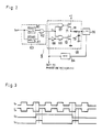
- Fig. 3 an output wave form chart of the principal signals appearing in the demodulated clock signal generator in Fig. 2
- Fig. 4 is a block diagram of a lock detector of Fig. 1
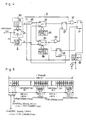
- Fig. 5 is a structural representation of frame data
- Fig. 6 is a graph showing the frequency spectrum of data signal
- Fig. 7 is a wave form chart of each component at the demodulated clock signal generator for explanation of the invention
- Fig. 8 is a block diagram of an improved demodulated clock signal generator of the invention in Fig. 2
- Fig. 9 is a block diagram of a second embodiment of the motor velocity control circuit of the invention
- Fig. 10 is a block diagram of a third embodiment of the invention
- Fig. 11 is a block diagram of a modification of the embodiment shown in Fig. 10.
- reference numeral 1 designates a pickup which projects a laser ray to a disc 2 to reproduce information recorded thereon.
- a data signal So detected by the pickup 1 is given to a demodulator 5 and a demodulated clock signal generator 6 through a radio frequency amplifier 3 and a wave-form shaping circuit 4.
- the demodulated clock signal generator 6 generates a demodulated clock frequency (of 4.3218 MHz) signal S 1 synchronized with the data signal So, the generated pulse output being given to the demodulator 5 in which the data signal So is detected as to its length on the basis of demodulated signal S,, thereby outputting binary digit data corresponding to length of data signal So.
- the data detected by the pickup 1 is defined to be of 3 to 11 bits of reference frequency (4.3218 MHz) corresponding to the signal level, whereby the demodulator 5 outputs the binary digit data corresponding to length of data signal So, i.e., signal level.
- Reference 7 designates an analog-digital converter for converting the binary digital data from the demodulator 5 into an analog signal which is amplified by an amplifier (not shown) and thereafter reproduced by a loud-speaker.
- Reference numeral 8 designates a lock detector which is given the data signal So and demodulated signal S 1 in synchronism therewith and detects the predetermined linear velocity rotation of disc 2.
- Numeral 9 designates a reference oscillator for generating the reference frequency (4.3218 MHz) signal, the output of oscillator 9 being divided by 160 by a frequency divider 10 to thereby feed a reference signal of about 27 kHz to a phase comparator 11.
- Numeral 12 designates a switching control circuit comprising a NAND gate 13 whose one input is given the demodulated clock signal S 1 and the other input is given the output of lock detector 8, a NAND gate 14 whose one input is given the data signal So and the other input is given an inverted output of lock detector 8, and a NAND gate 15 receiving the outputs of NAND gates 13 and 14, the switching control circuit 12 being adapted to output either the demodulated clock signal S 1 or the data signal So responsive to the output of lock detector 8.
- 16 designates a flip-flop which is reset by operating a play key 17 and set by operating a stop key 18 and stores the memory state
- 19 designates a programmable divider which is set to the dividing ratio data stored in ROM20, corresponding to dividing ratio "100", upon operation of a stop key 18 and is set by a selector 23 to the outputs of ROMs 21 and 22, in which the dividing ratio data "16" and "160" are stored upon operation of a play key 17.
- the selector 23 comprises an AND gate 24 receiving at the first input the Q output of flip-flop 16 and at the second input the output of lock detector 8 and an AND gate 25 receiving at the first input thereof the Q output of flip-flop and at the second input the inverted output of lock detector 8, and selects ROMs 21 and 22 responsive to the output of lock detector 8 to thereby select the dividing data to be set in the programmable divider 19.
- a phase comparator 11 receives the outputs of dividers 10 and 19 so as to generate an error voltage corresponding to the phase difference between both inputs.
- 26 designates a low-pass filter which generates a DC voltage corresponding to the error voltage from the phase comparator 11, and the output thereof is supplied to drive circuit 27 to control the number of rotations of motor 28.
- reference numerals 29 and 30 designate OR gates 31 and 32 designate inverters.
- Fig. 2 is a block diagram of the demodulated clock signal generator 6 shown in Fig. 1.
- the demodulated clock signal generator 6 comprises: a pulse oscillator 63 comprising a one shot multivibrator 60 operating at the leading edge of data signal detected by the pickup 1, a one shot multivibrator 61 operating at the trailing edge of the same, and an OR gate 62 given the outputs of both multivibrators 60 and 61; a phase comparator 65 receiving the output S 2 of pulse oscillator 63 and that S 1 of a voltage control oscillator 64 multivibrating at a frequency near the reference frequency; and a low-pass filter 66.
- the phase comparator 65 comprises a NAND gate 67 supplied at one input with the output S 2 of pulse oscillator 63 and at the other input directly with the output S 1 of voltage control oscillator 64, and AND gate 69 receiving the output S, through an inverter 68, and a charge pump 70 composed of a P-channel field-effect transistor (FET)71 supplied at the gate electrode with the output of NAND gate 67, and a N-channel FET 72 supplied at the gate electrode with the output of AND gate 69, so that charge-discharge control of a capacitor 73 connected between the node of FETs 71 and 72 and earth controls the voltage across the terminals of capacitor 73.
- FET field-effect transistor
- the data signal So detected by the pickup 1, when given to the demodulated clock signal generator 6, allows the phase comparator 65 to phase-compare the output S 2 of one shot multivibrator 60 operating at the leading edge of data signal So with that 5 1 of voltage control oscillator 64 in multivibration, at which time if both the outputs are locked in phase, the phase comparator 65, as shown in Fig. 3, detects by the NAND gate 67 the coincidence of output S 2 of one shot multivibrator 60 with that S 1 of voltage control oscillator 64.
- the P-channel FET 71 is conductive to charge the capacitor 73
- the coincidence of output S 2 of one shot multivibrator 60 with inverted output 9 1 of voltage control oscillator 64 is detected subsequently by the AND gate 69 and thus the N-channel FET 72 is conductive to discharge the capacitor 73; thus the time periods for discharge and charge, when phase is locked, become the same, whereby the capacitor 73 consequently is not changed in potential.
- phase shifts when the phase shifts, a difference is produced between the periods of time for charge and discharge so as to change the potential of capacitor 73 so that a voltage corresponding to the voltage difference is given to the voltage control oscillator 64 through the low-pass filter 66, thereby controlling the frequency of voltage control oscillator 64 to restore zero phase difference. Also, even at the trailing edge of data signal So, the aforesaid phase comparison is carried out between the output 5 2 of one shot multivibrator 61 and the oscillation frequency S 1 of voltage control oscillator 64 to thereby carry out phase matching of voltage control oscillation frequency and data signal So, thus obtaining from the voltage control oscillator 64 the demodulated clock signal synchronized with data signal So.
- reference numeral 80 designates a frame synchronous signal detector detecting the frame synchronous signal pattern, i.e., the 24 bit frame synchronous signal pattern, of data signal reproduced from the disc 2.
- the detector 80 comprises, for example, a 24 bit shift register 81 and a coincidence circuit 82 whereby specific data set to the coincidence circuit 82, if coincident with each other, generate a coincidence output "CO".
- Reference numerals 83 and 84 designate programmable down counters having preset enable terminals (PE) preset by the output of an OR gate 85 and clock pulse input terminals (CP) receiving the demodulated clock signal S,.
- Reference numeral 90 designates an AND gate whose one input receives the output of frame synchronous signal detector 80 and the other input the output Q of flip-flop 87, and 91 designates a flip-flop having a set terminal S receiving the output of AND gate 90 and a reset terminal R receiving the output Q of programmable down counter 84.
- the Q output of flip-flop 91 is supplied to the switching control circuit 12 in Fig. 1 through a time constant circuit 92 comprising an integration circuit.
- Reference numeral 93 designates a D-flip-flop which has a data input terminal D receiving the output of AND gate 90 and a clock pulse input terminal CP receiving the demodulated clock signal S, and supplies its Q output as a second input to OR gate 89. Also, the programmable down counters 83 and 84 are so constituted that the predetermined number is preset by the down count output Q of "598" through OR gate 85.
- the frame data as shown in Fig. 5, comprises the synchronous pattern signal bit of 24 bits absolutely not-appearing in EPM (Eight to Fourteen Modulation) at an information unit of 588 bits, the information bit of 336+72 bits (for connection), and the error correction bit of 112+24 bits (for connection), so that the data comprises 14 bits and between the data blocks is inserted the channel bit of 3 bits.
- EPM Eight to Fourteen Modulation
- the frame data shown in Fig. 5 when fed successively to the frame synchronous signal detector 80, is shifted successively and stored on the basis of demodulated clock signal S i .
- the coincidence output logic "1" is sent out by detecting the 24 bit frame synchronizing signal, the longest synchronous signal of data signal absolutely not appearing in EFM.
- the coincidence signal logic "1” sent out enables the programmable down counters 83 and 84 to be preset, whereby the predetermined number setting circuits 86 and 88 preset the predetermined numbers respectively.
- the logic "1" signal is generated from the lock detector 8 for the time period in which the time constant circuit 92 maintains the voltage and the demodulated clock signal S 1 is given to the programmable divider 19.
- the output of lock detector 8 is inverted to whereby the output of switching control circuit 12 is switched to the data signal So.
- the data signal So detected by the pick-up 1, as shown in Fig. 6, has frequency components of about 400 to 500 kHz at both sides of a center frequency of about 430 kHz (half width: lower limit 355 kHz and upper limit 535 kHz). This is based on the coding system of compact disc digital audio system and the frequency component at the peak 430 kHz is the signal corresponding to magnitude of 5 bits: As a result, continuously, the disc 2 reproduces the frequency component of 430 kHz with high probability and during a large percentage of time, whereby the motor can be driven and controlled paying attention to the 430 kHz frequency.
- the data signal detected by the pickup 1 following the start of motor 28 and divided by sixteen by the dividing data "16" of divider 19 is given to the phase comparator 11.
- the divider output based on the coding system of compact disc digital audio system, that is, the divided output of divider 19 is still lower than the reference signal of 27 kHz, thereby further increasing the number of rotations of motor 28.
- the voltage controlled oscillator 64 which has a follow-up capacity of only several percent with respect to fluctuation of the data signal So begins to receive the data signal So in the range of its follow-up capacity, and subsequently the demodulated clock signal generator 6 generates the demodulated clock signal S 1 synchronized with the data signal So. Then, in the lock detector 8 shown in Fig.
- the data signal So is given successively to the shift register 81 on the basis of the demodulated clock signal S i , the coincidence output "CO" of frame synchronous signal by the coincidence circuit 82 supplies the logic "1" output to AND gate 90, the OR gate 85 sets the predetermined numbers to the programmable down counters 83 and 84, and the down count outputs thereof set the flip-flop 87. Then, AND is effected so that the output of AND gate 90 sets the flip-flop 91, whereby the lock detector 8 outputs the signal of logic "1".
- the dividing ratio data "160" of ROM 22 is read out from the selector 23, the same is set in the programmable divider 19, and the output of switching control circuit 12 is switched to send out the demodulated clock signal S 1'
- the plase comparator 11 compares the output of voltage controlled oscillator 64 with that of reference oscillator 9 comprising a quartz oscillator so that the motor drive circuit 27 controls corresponding to the comparison error output the number of rotations of motor 28 driving the disc 2 to make the demodulated clock signal to coincide with the reference signal of 4.3218 MHz from the reference oscillator 9.
- speed control of motor 28 for proper length of data signal So detected by pickup 1 means that the number of rotations of the same is controlled to keep constant the linear velocity.
- the demodulator 5 is given the demodulated clock signal S, of 4.3218 MHz in synchronism with'data signal So, length of data signal So detected by the pickup 1 being detected to be demodulated in binary digit data.
- the flip-flop 16 is set, its Q output of logic "1" being given to the switching control circuit 12 through OR gate 30. Consequently, the demodulated clock signal S, of demodulated clock signal generator 6 is sent out from the output of switching control circuit 12. Also, the operation of stop key 18 sets to the programmable divider 19 the dividing ratio: logic "100" from ROM 20. The programmable divider 19 feeds to the phase comparator 11 the output of voltage controlled oscillator 64 multivibrating in the neighborhood of 4.3218 MHz divided by 100, that is an output of 43 kHz.
- the frequency of 43 kHz is far leading in phase and frequency with respect to the reference signal of 27 kHz, which is equivalent to rapid velocity of motor 28, so that the phase comparator 11 generates an error voltage for reducing the velocity, whereby the motor 28 is rapidly decelerated equivalent to a braking action.
- the voltage controlled oscillator 64 follows the lowered data signal to lower to the lower limit of the range of follow-up capacity, but the value is several percent of the central frequency, for example 4 MHz, so that the divided output has a higher level in comparison with the reference value, thereby further exerting the braking action to rapidly put the motor in the stop condition.
- While the embodiment is constructed to change the dividing ratio of the divider 19 which divides the output of switching control circuit 12 it may alternatively be constructed to change the dividing ratio of divider 10 which divides the output of reference oscillator 9.
- the frame synchronous signal in the data signal detected from the disc is detected to indicate the constant velocity rotation of the motor.
- the frequency of 430 kHz i.e. the main frequency component of the data signal on the basis of coding system of compact disc digital audio system, is detected from the high frequency amplifier 3 through a means, such as a filter, which, when used as the lock detector indicating the motor rotating at constant speed, is simple because of no particular extraction of synchronous signal.
- the first embodiment of the invention performs rotational velocity control of motor during (i) the starting, (ii) rotation at constant linear velocity, (iii) stop and (iv) variation of rotational velocity of motor.
- the data signal reproduced from the disc is compared in phase with the output of the reference oscillator, and paying attention to the frequency component of 430 kHz being the mean output on the basis of coding system of compact disc digital audio system, this frequency is divided by a proper value and phase-compared with the divided output of the reference oscillator, whereby the rotation of motor is controlled up to the predetermined linear velocity, where accurate data signal can be extracted from the disc.
- the demodulated clock signal synchronized with the data signal is phase-compared with the reference signal of reference oscillator, thereby controlling the disc to be driven at constant linear velocity.
- the first embodiment of the invention uses the switching control circuit 12, thereby solving all the above problems.
- the voltage controlled oscillator has a sufficient follow-up capability with respect to variations of the data signal So, so that the demodulated clock signal 8, in synchronism with the data signal phase-compared with the output of reference oscillator 9 by the phase comparator 11, is used to control the disc 2 not only when driven at constant linear velocity but also during the starting of motor.
- An improved demodulated clock signal generator 600 is shown in Fig.
- reference numeral 74 designates a voltage divider connected to the output line of low-pass filter 66, the voltage divider 74 comprising a resistance R, grounded at one end and having at the other end a movable contact 75, and resistances R 2 and R 3 having fixed contacts 76 and 75 and connected in parallel to the output of low-pass filter 66.
- the resistance value is set to be R 2 ⁇ R 3 and a relay 78 energized by the lock detection output from the lock detector 8 is adapted to switch the contact 75 toward the resistance R 3 .
- the voltage controlled oscillator 64 when the motor 28 starts, is controlled by a sufficiently large partial voltage V.R 1 /(R 1 +R 2 ) determined by a relatively small resistance R 2 and by resistance R i , and is successively switched to relatively larger resistance -R 3 corresponding to the switching signal from lock detector 8, thus operating at small amplitude V - R 1 /(R 1 +R 3 ).
- Fig. 9 is a block diagram of a motor speed control circuit using the improved demodulated clock signal generator 600, in which the components identical with those in Fig. 1 are designated by the same reference numerals.
- Reference numeral 210 designates a ROM to which the dividing ratio data "180" is set, so that when a play key 17 is operated the output is read out to be set in the programmable divider 19.
- 200 designates a ROM to set the dividing ratio data "100" so that when a stop key 18 is operated the dividing ratio "100” is set in the divider 19.
- the dividing ratio data "180" set to ROM 210 is set to the programmable divider 19 by operation of play key 17 so that the output of voltage control oscillator 64 multivibrating in the neighborhood of 4.3218 MHz is divided by the dividing data "180".
- the output of frequency divider 19 is about equal to the reference signal so that the phase comparator 11 generates no error output, but if the motor rotates out of the predetermined speed, the demodulated clock signal frequency generated by the demodulated clock signal generator 600 shifts from the predetermined 4.3218 MHz, whereby an error voltage corresponding to the phase difference is generated from the phase comparator 11 to control the motor 28.
- the speed change of motor 28 restores the demodulated clock signal frequency to the predetermined 4.3218 MHz and the speed control of the same continued until no error output is generated from the phase comparator 11, thus carrying out the phase comparison constantly during the reproduction by the disc 2 and controlling the motor 28 at constant linear speed.
- ROM 200 feeds the dividing ratio "100" into the frequency divider 19 to rapidly lower the speed of motor 28 in a manner equivalent to a braking action, thus instantaneously stopping the motor 28 and keeping it stationary.
- FIG. 10 A third embodiment of the invention is shown in Fig. 10, in which reference numeral 190 designates a frequency divider which is given the data signal So output from the high frequency amplifier 3 whose dividing ratio is set to "16", 100 designates a frequency divider which divides the output of reference oscillator 9 composed of a quartz oscillator generating the reference oscillation signal of 4.3218 MHz and is constituted to change the dividing ratio during the play and the stop, and 2100 and 2000 designate ROMs storing the dividing ratio data for frequency divider 100.
- ROM 2100 is adapted to feed the dividing ratio data "160" into the frequency divider 100, when the play key 17 is operated.
- the dividing ratio data "1600” is stored in ROM 2000 and set to the frequency divider 100 by operating the stop key 18.
- the dividing ratio of divider 100 is set normally to "160", whereby frequency divider 100 outputs the reference signal of 27 kHz.
- ROM 2100 feeds the dividing ratio data of "160" into the frequency divider 100, and a reference signal of 27 kHz corresponding to reference signal of 4.3218 MHz divided by 160 is given from the divider 100 to the phase comparator 11, but since the disc 2 is not yet rotating, the phase comparator 11 is not receiving a divided output of data signal So from frequency divider 190, and therefore outputs an error signal to increase the number of rotations of motor 28, whereby the motor drive circuit 27 rapidly accelerates the rotation of the motor to obtain a short starting time.
- phase comparator 11 When the data signal So is detected by the pickup 1 due to rotation of disc 2 following rotation of motor 28, the phase comparator 11 receives a signal of about 27 kHz from the data signal So divided by 16 in the frequency divider 190 to thereby carry out phase comparison between this signal of about 27 kHz and the reference signal.
- ROM 2000 feeds the dividing ratio data "1600" into the frequency divider 100, whereby an output of 2.7 kHz is obtained from the frequency divider 100 and given to the phase comparator 11.
- the output of frequency divider 190 is of 27 kHz and leads in phase with respect to the reference signal. This is equivalent to the speed of motor 28 being too high, whereby the motor 28 is rapidly reduced in speed or braked, thus instantaneously stopping the motor and keeping it stationary.
- frequency divider 190 is lowered as the frequency of data signal So detected by pickup 1 is lowered following the reduced rotational speed, but since random pulses are generated the output of divider 190 will not become completely zero. Therefore, the dividing ratio of frequency divider 190 when the motor stops, needs only be decided in consideration of the random pulse frequency.
- the dividing ratio of divider 100 during the motor stop is set higher to thereby lower the reference signal
- the reference signal may also be cut off.
- this embodiment instead of changing the dividing ratio of the divider 100 for dividing the reference signal, may alternatively be constructed to change the dividing ratio of divider 190 dividing the data signal.
- frequency dividers 1000 and 1900 having a fixed preset dividing ratio are used to control the motor at the starting, constant speed rotation, and stop.
- the frequency divider 1900 is given the data signal So output from the high frequency amplifier 3 through a changeover switch 33 and is set to the dividing ratio "16".
- the frequency divider 1000 divides the output of reference oscillator 9 comprising a quartz oscillator generating reference oscillation signal of 4.3218 MHz and now is set to the dividing ratio of "160' and is thus generating a reference signal of 27 kHz.
- the output of reference oscillator 9 can also be given to the other stationary contact 33c of the changeover switch 33 and then to the divider 1900.
- the changeover switch 33 is switched normally to the stationary contact 33b and adapted to be switched to the other stationary contact 33c by operation of stop key 18.
- a play key (not shown) at first is operated and the frequency divider 1000 feeds into the phase comparator 11 a reference signal of 27 kHz corresponding to the reference signal of 4.3218 MHz divided by 160, but since the disc 2 is not rotated, the phase comparator 11 is not receiving a divided output from divider 1900. Therefore, the phase comparator 11 generates an error output to increase the rotation of motor 28, whereby the number of rotations thereof is rapidly increased by the motor drive circuit 27 and a short starting time is obtained, thus driving the disc 2 at constant linear velocity.
- the stop key 18 is operated to switch the contact 33a to the other stationary contact 33c at the changeover switch 33a, whereby the reference signal of reference oscillator 9 is divided by 16 to obtain 270 kHz.
- the phase comparator 11 generates error voltage so as to lower the motor 28 speed, thereby rapidly reducing the speed of motor 28 equivalent to a braking action thus instantaneously stopping the motor 28 and keeping it stationary.
- the dividing ratio of each frequency divider 1000 or 1900, which was described to be 160 and 16, is not limited thereto and needs only be decided corresponding to the frequency for phase comparison.
- the motor speed control circuit of the invention comprises a switching control circuit for alternatively switching the data signal detected by the pickup or a demodulated clock signal synchronized with the data signal to a divided output, a reference oscillator for generating the reference oscillation signal, phase comparison means comparing in phase the output of reference oscillator with that of the switching control circuit, and means for controlling the motor to be driven corresponding to an error output from the phase comparison means.
- the output obtained by dividing the data signal detected by the pickup is phase-compared with the output of reference oscillator and the error output controls the number of rotations of motor, whereby the rotation of disc can be controlled to be driven at constant linear velocity.
- the data signal detected by the disc, when the motor starts is divided into proper values, the divided output being phase-compared with the reference signal, thereby enabling the starting of motor.
- the number of rotations of motor is included sufficiently within a range of several percent of the predetermined number of rotations of the same at constant linear velocity thereof, whereby the phase comparison of the demodulated clock signal in synchronism with the data signal with reference signal can drive the motor at constant linear velocity.
- the switching control circuit switches the signal given to the phase comparison means from the data signal detected properly from the disc to the demodulated clock signal synchronized with the data signal to enable the starting as well as the driving of the motor at constant linear velocity, thereby facilitating the digital process and integration.
- the disc can be driven under control of the data signal up to near the predetermined linear velocity rotation, and when it reaches the neighborhood thereof, the switching control circuit automatically switches the data signal to the demodulated clock signal which has a smaller fluctuation range so that the demodulated signal is phase-compared with the reference signal, thereby obtaining rotation of motor with smaller variation and improving the reproduction characteristic.
- the voltage controlled oscillator of the demodulated clock signal generator shifts from the phase synchronizing loop to the limit of its follow-up capability.
- the output given to the phase comparator from the switching control circuit is switched to the divided output of data signal detected from the disc, so that the motor is controlled in rotation by the divided output of the frequency spectrum of data signal, whereby the number of rotations of motor is restored with ease into the range of several percent from the predetermined number of rotations thereof at constant linear velocity.
- the motor speed control circuit of the invention is of extremely high reliability.
- the dividing ratio of the frequency divider for the signal to be phase-compared is changed when the motor starts, rotates at constant speed and stops, thereby obtaining a short starting time of motor and a rapid stop thereof.
- the frequency to be used for phase comparison is set out of the audio frequency range whereby the reproduction characteristic is not adversely effected.
- the disc since the synchronous signal in the disc is not used for drive control of motor at constant linear velocity, the disc is controllable to be driven at constant linear speed independently of lack of synchronous signal in the disc.
- This invention is applicable to a speed control circuit for a motor to rotate a rotary medium at constant linear velocity.
- the data signal reproduced from the disc on the basis of coding method of compact disc digital audio system is distributed over about 400-500 kHz around the frequency component of about 430 kHz frequency component (in other words, the peak of 430 kHz frequency component corresponding to magnitude of 5 bits of reference signal)
- the embodiments of the invention phase-compare the reference signal with the data signal reproduced from the disc and including the frequency spectrum reproduced with high generation percentage in probability, thereby having controlled the motor to be driven at constant linear velocity.
- the invention is applicable to the rotary medium, such as video disc, on which data signal is recorded at constant linear velocity when recorded.
- this invention drives and controls the motor by the phase comparison means in such a manner that the demodulated clock signal of 4.3218 MHz corresponding to the minimum information bit in synchronism with the data signal reproduced by the disc corresponds to the reference frequency signal (of 4.3218 MHz) of reference oscillator in a ratio of 1 to 1.
- the reference frequency signal corresponding to the above information bit is set
- the demodulated clock signal in synchronism with data signal reproduced from the rotary medium is constituted by the oscillator in multivibration in the neighborhood of the reference frequency signal
- phase comparison means controls in comparison the demodulated clock signal in synchronism with the data signal demodulated by the oscillator so that the clock signal corresponds at a ratio of 1 to 1 to the reference frequency signal of the reference oscillator
- the control output of the comparison means drives the motor, thereby enabling rotational control of the rotary medium at constant linear velocity.
- the rotary medium on which the data signal is recorded at integer times the minimum information bit is rotatably controllable at constant linear velocity by the circuit of the invention.
- the rotary medium having the signal recorded thereon at integer times the minimum information bit and data signal recording method having the frequency component of the peak component when the number of rotations of motor largely varies, or in some cases, phase-compares the data signal with the reference signal paying attention to the peak component at the recorded data signal to thereby drive-control the motor and rotatably control the rotary medium at constant linear velocity.
- the demodulated signal synchronized with the recorded data signal is phase-compared with the reference frequency signal to thereby drive-control the motor and rotatably control the rotary medium at constant linear velocity.
- Such method can further preferably rotatably control the rotary medium at constant linear velocity.
- the rotary medium recording thereon data signal integer times as large as the minimum information bit by use of the recording method having the frequency component of the peak component is rotatably controllable at constant linear velocity.
Landscapes
- Engineering & Computer Science (AREA)
- Power Engineering (AREA)
- Rotational Drive Of Disk (AREA)
Claims (8)
Applications Claiming Priority (8)
| Application Number | Priority Date | Filing Date | Title |
|---|---|---|---|
| JP44252/82 | 1982-03-18 | ||
| JP57044252A JPS58159683A (ja) | 1982-03-18 | 1982-03-18 | モ−タ−速度制御回路 |
| JP57070673A JPS58190292A (ja) | 1982-04-26 | 1982-04-26 | モ−タ−速度制御回路 |
| JP70673/82 | 1982-04-26 | ||
| JP70674/82 | 1982-04-26 | ||
| JP57070674A JPS58190293A (ja) | 1982-04-26 | 1982-04-26 | モ−タ−速度制御回路 |
| JP3653/83 | 1983-01-12 | ||
| JP58003653A JPS59129593A (ja) | 1983-01-12 | 1983-01-12 | モ−タ−速度制御回路 |
Publications (3)
| Publication Number | Publication Date |
|---|---|
| EP0103028A1 EP0103028A1 (de) | 1984-03-21 |
| EP0103028A4 EP0103028A4 (de) | 1984-07-26 |
| EP0103028B1 true EP0103028B1 (de) | 1986-09-03 |
Family
ID=27453917
Family Applications (1)
| Application Number | Title | Priority Date | Filing Date |
|---|---|---|---|
| EP83900853A Expired EP0103028B1 (de) | 1982-03-18 | 1983-03-14 | Schaltung zur geschwindigkeitskontrolle eines motors |
Country Status (4)
| Country | Link |
|---|---|
| US (1) | US4613799A (de) |
| EP (1) | EP0103028B1 (de) |
| DE (1) | DE3365787D1 (de) |
| WO (1) | WO1983003325A1 (de) |
Cited By (1)
| Publication number | Priority date | Publication date | Assignee | Title |
|---|---|---|---|---|
| EP0536699A3 (en) * | 1991-10-07 | 1993-06-09 | Chuo Denki Co., Ltd. | Disk playback apparatus |
Families Citing this family (10)
| Publication number | Priority date | Publication date | Assignee | Title |
|---|---|---|---|---|
| JPS60173767A (ja) * | 1984-02-20 | 1985-09-07 | Sony Corp | 光学式ディスク装置 |
| US4855654A (en) * | 1985-03-16 | 1989-08-08 | Canon Kabushiki Kaisha | Rotary body drive device |
| JPS61211711A (ja) * | 1985-03-16 | 1986-09-19 | Pioneer Electronic Corp | 位相比較器 |
| US4816937A (en) * | 1985-10-17 | 1989-03-28 | Canon Kabushiki Kaisha | Recording and/or reproduction apparatus capable of retaining start up information |
| EP0237682B1 (de) * | 1985-12-24 | 1991-02-27 | Kabushiki Kaisha Toshiba | Steuersystem für ein Gerät zur Wiedergabe optischer Informationen |
| JP2523609B2 (ja) * | 1987-03-31 | 1996-08-14 | 株式会社東芝 | モ−タ−の速度制御装置 |
| JP2638079B2 (ja) * | 1988-05-30 | 1997-08-06 | ソニー株式会社 | 光デイスク装置 |
| DE4102796A1 (de) * | 1991-01-31 | 1992-08-06 | Thomson Brandt Gmbh | Verfahren zur verkuerzung der zugriffszeit |
| JP2002034286A (ja) * | 2000-07-17 | 2002-01-31 | Nec Corp | Hブリッジ型モータ駆動回路 |
| CN107093539B (zh) * | 2016-12-26 | 2018-12-28 | 中国工程物理研究院应用电子学研究所 | 一种太赫兹相速渐变折叠波导振荡器 |
Family Cites Families (19)
| Publication number | Priority date | Publication date | Assignee | Title |
|---|---|---|---|---|
| US3097267A (en) * | 1958-08-08 | 1963-07-09 | Ampex | Tape recording and/or reproducing system and method |
| US3268788A (en) * | 1963-01-09 | 1966-08-23 | Minnesota Mining & Mfg | Phase difference speed control system |
| US3361949A (en) * | 1964-08-24 | 1968-01-02 | Continental Oil Co | Motor control servo system |
| US3400314A (en) * | 1965-05-27 | 1968-09-03 | Gen Electric | Numerical positioning control system |
| US3495208A (en) * | 1966-04-04 | 1970-02-10 | Krupp Gmbh | Method of and apparatus for regulating and maintaining constant the speed of driving motors |
| US3500162A (en) * | 1968-03-27 | 1970-03-10 | Sangamo Electric Co | System for providing dc values representative of phase difference |
| US3753067A (en) * | 1972-05-17 | 1973-08-14 | Peripheral Systems Corp | Motor speed regulation system |
| US3967177A (en) * | 1974-11-14 | 1976-06-29 | Addressograph Multigraph Corporation | Photocomposition machine |
| GB1527741A (en) * | 1975-03-25 | 1978-10-11 | Rca Corp | Brushless dc motor rotation control |
| JPS5222714A (en) * | 1975-08-14 | 1977-02-21 | Matsushita Electric Ind Co Ltd | Control device for rotary unit |
| JPS5274810A (en) * | 1975-12-18 | 1977-06-23 | Toshiba Corp | Motor controller |
| GB1572346A (en) * | 1976-03-19 | 1980-07-30 | Rca Corp | Velocity and phase control for a disc recording and reproducing apparatus |
| US4211967A (en) * | 1977-04-27 | 1980-07-08 | Matsushita Electric Industrial Co., Ltd. | Motor speed adjusting apparatus |
| US4314188A (en) * | 1979-03-15 | 1982-02-02 | Sperry Corporation | Stable subsynchronous drive system for gyroscope rotor |
| JPS5671856A (en) * | 1979-11-15 | 1981-06-15 | Sony Corp | Playback device of disc |
| JPS5671855A (en) * | 1979-11-15 | 1981-06-15 | Sony Corp | Playback device of disc |
| JPS57189587A (en) * | 1981-05-15 | 1982-11-20 | Sanyo Electric Co Ltd | Controlling circuit for motor |
| JPS5843196A (ja) * | 1981-09-07 | 1983-03-12 | Sanyo Electric Co Ltd | モ−タ制御方法 |
| JPS58159682A (ja) * | 1982-03-18 | 1983-09-22 | Sanyo Electric Co Ltd | モ−タ−速度制御回路 |
-
1983
- 1983-03-14 EP EP83900853A patent/EP0103028B1/de not_active Expired
- 1983-03-14 US US06/545,393 patent/US4613799A/en not_active Expired - Lifetime
- 1983-03-14 DE DE8383900853T patent/DE3365787D1/de not_active Expired
- 1983-03-14 WO PCT/JP1983/000079 patent/WO1983003325A1/ja not_active Ceased
Cited By (1)
| Publication number | Priority date | Publication date | Assignee | Title |
|---|---|---|---|---|
| EP0536699A3 (en) * | 1991-10-07 | 1993-06-09 | Chuo Denki Co., Ltd. | Disk playback apparatus |
Also Published As
| Publication number | Publication date |
|---|---|
| WO1983003325A1 (fr) | 1983-09-29 |
| EP0103028A1 (de) | 1984-03-21 |
| DE3365787D1 (en) | 1986-10-09 |
| EP0103028A4 (de) | 1984-07-26 |
| US4613799A (en) | 1986-09-23 |
Similar Documents
| Publication | Publication Date | Title |
|---|---|---|
| EP0081757B1 (de) | Schaltungsanordnung zur Gewinnung oder Wiederherstellung von Rahmensynchronisiersignalen | |
| US4338683A (en) | Videodisc player with constant turntable velocity | |
| EP0182701B1 (de) | Phasenregelschleife zur MFM-Datenaufzeichnung | |
| EP0096106A1 (de) | PLL-Steuerkreis | |
| US4613799A (en) | Motor velocity control circuit | |
| CA1171174A (en) | Servo system | |
| JPH10257041A (ja) | フェイズロックドループ回路及び再生装置 | |
| EP0425475B1 (de) | System zur Übertragung und Erkennung von Daten | |
| JP3607048B2 (ja) | ディスク再生装置及びデータスライス回路 | |
| EP0597372B1 (de) | Vorrichtungen zur Wiedergabe eines digitalen Signales, integrierte Schaltungen dafür sowie Verfahren zur Wiedergabe eines digitalen Signales | |
| EP1118991B1 (de) | Drehservosteuerschaltung | |
| JPS5989038A (ja) | フエ−ズ・ロツクド・ル−プ回路 | |
| US5260841A (en) | Clock extracting circuit | |
| GB2197144A (en) | Bit clock signal generator for a digital signal demodulator | |
| JP2833540B2 (ja) | ディジタル放送用衛星放送受信機 | |
| JPH0546030B2 (de) | ||
| JP3456359B2 (ja) | ディジタル信号再生装置 | |
| JP2584352B2 (ja) | インターフェイス回路 | |
| JP3318935B2 (ja) | デジタル信号記録装置 | |
| KR200144434Y1 (ko) | 레이저 디스크 플레이어의 디스크 모터 회전 제어회로 | |
| JPH07141781A (ja) | データ再生用pll回路の制御装置 | |
| EP0771111A2 (de) | Rasterpuls-Erzeugungsanlage für Standard-Auflösung-Fernsehkassettenaufnehmer | |
| JPH04271635A (ja) | インターフェイス回路及びこれに用いる位相ロックループ | |
| JPH0526264B2 (de) | ||
| JPS6083258A (ja) | デイスク駆動方式 |
Legal Events
| Date | Code | Title | Description |
|---|---|---|---|
| PUAI | Public reference made under article 153(3) epc to a published international application that has entered the european phase |
Free format text: ORIGINAL CODE: 0009012 |
|
| 17P | Request for examination filed |
Effective date: 19831117 |
|
| AK | Designated contracting states |
Designated state(s): DE GB |
|
| GRAA | (expected) grant |
Free format text: ORIGINAL CODE: 0009210 |
|
| AK | Designated contracting states |
Kind code of ref document: B1 Designated state(s): DE GB |
|
| REF | Corresponds to: |
Ref document number: 3365787 Country of ref document: DE Date of ref document: 19861009 |
|
| PLBE | No opposition filed within time limit |
Free format text: ORIGINAL CODE: 0009261 |
|
| STAA | Information on the status of an ep patent application or granted ep patent |
Free format text: STATUS: NO OPPOSITION FILED WITHIN TIME LIMIT |
|
| 26N | No opposition filed | ||
| PGFP | Annual fee paid to national office [announced via postgrant information from national office to epo] |
Ref country code: DE Payment date: 20010306 Year of fee payment: 19 |
|
| PGFP | Annual fee paid to national office [announced via postgrant information from national office to epo] |
Ref country code: GB Payment date: 20010314 Year of fee payment: 19 |
|
| REG | Reference to a national code |
Ref country code: GB Ref legal event code: IF02 |
|
| PG25 | Lapsed in a contracting state [announced via postgrant information from national office to epo] |
Ref country code: GB Free format text: LAPSE BECAUSE OF NON-PAYMENT OF DUE FEES Effective date: 20020314 |
|
| PG25 | Lapsed in a contracting state [announced via postgrant information from national office to epo] |
Ref country code: DE Free format text: LAPSE BECAUSE OF NON-PAYMENT OF DUE FEES Effective date: 20021001 |
|
| GBPC | Gb: european patent ceased through non-payment of renewal fee |
Effective date: 20020314 |