EP0098177B1 - Scanning electron-beam exposure system - Google Patents
Scanning electron-beam exposure system Download PDFInfo
- Publication number
- EP0098177B1 EP0098177B1 EP19830303812 EP83303812A EP0098177B1 EP 0098177 B1 EP0098177 B1 EP 0098177B1 EP 19830303812 EP19830303812 EP 19830303812 EP 83303812 A EP83303812 A EP 83303812A EP 0098177 B1 EP0098177 B1 EP 0098177B1
- Authority
- EP
- European Patent Office
- Prior art keywords
- area
- rectangular areas
- group
- rectangular
- pattern
- Prior art date
- Legal status (The legal status is an assumption and is not a legal conclusion. Google has not performed a legal analysis and makes no representation as to the accuracy of the status listed.)
- Expired
Links
Images

Classifications
-
- B—PERFORMING OPERATIONS; TRANSPORTING
- B82—NANOTECHNOLOGY
- B82Y—SPECIFIC USES OR APPLICATIONS OF NANOSTRUCTURES; MEASUREMENT OR ANALYSIS OF NANOSTRUCTURES; MANUFACTURE OR TREATMENT OF NANOSTRUCTURES
- B82Y10/00—Nanotechnology for information processing, storage or transmission, e.g. quantum computing or single electron logic
-
- B—PERFORMING OPERATIONS; TRANSPORTING
- B82—NANOTECHNOLOGY
- B82Y—SPECIFIC USES OR APPLICATIONS OF NANOSTRUCTURES; MEASUREMENT OR ANALYSIS OF NANOSTRUCTURES; MANUFACTURE OR TREATMENT OF NANOSTRUCTURES
- B82Y40/00—Manufacture or treatment of nanostructures
-
- H—ELECTRICITY
- H01—ELECTRIC ELEMENTS
- H01J—ELECTRIC DISCHARGE TUBES OR DISCHARGE LAMPS
- H01J37/00—Discharge tubes with provision for introducing objects or material to be exposed to the discharge, e.g. for the purpose of examination or processing thereof
- H01J37/30—Electron-beam or ion-beam tubes for localised treatment of objects
- H01J37/302—Controlling tubes by external information, e.g. programme control
- H01J37/3023—Programme control
- H01J37/3026—Patterning strategy
-
- H—ELECTRICITY
- H01—ELECTRIC ELEMENTS
- H01J—ELECTRIC DISCHARGE TUBES OR DISCHARGE LAMPS
- H01J37/00—Discharge tubes with provision for introducing objects or material to be exposed to the discharge, e.g. for the purpose of examination or processing thereof
- H01J37/30—Electron-beam or ion-beam tubes for localised treatment of objects
- H01J37/317—Electron-beam or ion-beam tubes for localised treatment of objects for changing properties of the objects or for applying thin layers thereon, e.g. for ion implantation
- H01J37/3174—Particle-beam lithography, e.g. electron beam lithography
-
- H—ELECTRICITY
- H01—ELECTRIC ELEMENTS
- H01L—SEMICONDUCTOR DEVICES NOT COVERED BY CLASS H10
- H01L21/00—Processes or apparatus adapted for the manufacture or treatment of semiconductor or solid state devices or of parts thereof
- H01L21/02—Manufacture or treatment of semiconductor devices or of parts thereof
- H01L21/04—Manufacture or treatment of semiconductor devices or of parts thereof the devices having potential barriers, e.g. a PN junction, depletion layer or carrier concentration layer
- H01L21/18—Manufacture or treatment of semiconductor devices or of parts thereof the devices having potential barriers, e.g. a PN junction, depletion layer or carrier concentration layer the devices having semiconductor bodies comprising elements of Group IV of the Periodic Table or AIIIBV compounds with or without impurities, e.g. doping materials
- H01L21/30—Treatment of semiconductor bodies using processes or apparatus not provided for in groups H01L21/20 - H01L21/26
-
- H—ELECTRICITY
- H01—ELECTRIC ELEMENTS
- H01J—ELECTRIC DISCHARGE TUBES OR DISCHARGE LAMPS
- H01J2237/00—Discharge tubes exposing object to beam, e.g. for analysis treatment, etching, imaging
- H01J2237/30—Electron or ion beam tubes for processing objects
- H01J2237/317—Processing objects on a microscale
- H01J2237/3175—Lithography
- H01J2237/31761—Patterning strategy
- H01J2237/31764—Dividing into sub-patterns
-
- H—ELECTRICITY
- H01—ELECTRIC ELEMENTS
- H01J—ELECTRIC DISCHARGE TUBES OR DISCHARGE LAMPS
- H01J2237/00—Discharge tubes exposing object to beam, e.g. for analysis treatment, etching, imaging
- H01J2237/30—Electron or ion beam tubes for processing objects
- H01J2237/317—Processing objects on a microscale
- H01J2237/3175—Lithography
- H01J2237/31769—Proximity effect correction
-
- H—ELECTRICITY
- H01—ELECTRIC ELEMENTS
- H01J—ELECTRIC DISCHARGE TUBES OR DISCHARGE LAMPS
- H01J2237/00—Discharge tubes exposing object to beam, e.g. for analysis treatment, etching, imaging
- H01J2237/30—Electron or ion beam tubes for processing objects
- H01J2237/317—Processing objects on a microscale
- H01J2237/3175—Lithography
- H01J2237/31776—Shaped beam
Definitions
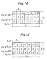
- the pattern generator 203A performs, an operation for generating the pattern 6 of the parameters (x o , y o , S x , Sy) shown in Fig. 1A so that the pattern 6 of the parameters is In this case, X 1 -6S ⁇ S. Therefore, the output of the comparator 307 changes so that the selector 308 selects the upper input thereof and the X-direction scanning and signal EX becomes logic "1". In this state, when the next pulse of the system clock signal CK1 is generated, a signal EX' becomes logic "1" so that X o is again stored in the register 301 and the value of the register 303 is changed from Y 0 to Y o +S.
- the pattern generator 203A performs an operation for generating the pattern 20 of the parameters (x o , y o , S x , Sy) shown in Fig. 1A so that the pattern 20 of the parameters is In this case, X,-6S ⁇ S and Y 1 -2S ⁇ S. Therefore, the outputs of the comparators 307 and 311 are both logic "1". As a result, an end signal EDI is transmitted to the CPU 201, thereby completing the exposure operation.
Landscapes
- Engineering & Computer Science (AREA)
- Chemical & Material Sciences (AREA)
- Nanotechnology (AREA)
- Analytical Chemistry (AREA)
- Physics & Mathematics (AREA)
- Manufacturing & Machinery (AREA)
- General Physics & Mathematics (AREA)
- Crystallography & Structural Chemistry (AREA)
- Condensed Matter Physics & Semiconductors (AREA)
- Computer Hardware Design (AREA)
- Microelectronics & Electronic Packaging (AREA)
- Power Engineering (AREA)
- Mathematical Physics (AREA)
- Theoretical Computer Science (AREA)
- Electron Beam Exposure (AREA)
Applications Claiming Priority (2)
| Application Number | Priority Date | Filing Date | Title |
|---|---|---|---|
| JP111534/82 | 1982-06-30 | ||
| JP57111534A JPS593923A (ja) | 1982-06-30 | 1982-06-30 | 電子ビ−ム露光方法 |
Publications (3)
| Publication Number | Publication Date |
|---|---|
| EP0098177A2 EP0098177A2 (en) | 1984-01-11 |
| EP0098177A3 EP0098177A3 (en) | 1986-06-04 |
| EP0098177B1 true EP0098177B1 (en) | 1989-03-22 |
Family
ID=14563780
Family Applications (1)
| Application Number | Title | Priority Date | Filing Date |
|---|---|---|---|
| EP19830303812 Expired EP0098177B1 (en) | 1982-06-30 | 1983-06-30 | Scanning electron-beam exposure system |
Country Status (3)
| Country | Link |
|---|---|
| EP (1) | EP0098177B1 (show.php) |
| JP (1) | JPS593923A (show.php) |
| DE (1) | DE3379487D1 (show.php) |
Families Citing this family (6)
| Publication number | Priority date | Publication date | Assignee | Title |
|---|---|---|---|---|
| US4818885A (en) * | 1987-06-30 | 1989-04-04 | International Business Machines Corporation | Electron beam writing method and system using large range deflection in combination with a continuously moving table |
| US4816692A (en) * | 1987-07-08 | 1989-03-28 | International Business Machines Corporation | Pattern splicing system and method for scanning of electron beam system |
| JPH01286310A (ja) * | 1988-05-12 | 1989-11-17 | Nec Corp | 荷電ビーム露光方法 |
| DE69030243T2 (de) * | 1989-12-21 | 1997-07-24 | Fujitsu Ltd | Verfahren und Gerät zur Steuerung von Ladungsträgerstrahlen in einem Belichtungssystem mittels Ladungsträgerstrahlen |
| US5393987A (en) * | 1993-05-28 | 1995-02-28 | Etec Systems, Inc. | Dose modulation and pixel deflection for raster scan lithography |
| US5624774A (en) * | 1994-06-16 | 1997-04-29 | Nikon Corporation | Method for transferring patterns with charged particle beam |
Family Cites Families (4)
| Publication number | Priority date | Publication date | Assignee | Title |
|---|---|---|---|---|
| US4099062A (en) * | 1976-12-27 | 1978-07-04 | International Business Machines Corporation | Electron beam lithography process |
| JPS5493364A (en) * | 1977-12-30 | 1979-07-24 | Fujitsu Ltd | Exposure system for electron beam |
| JPS5831728B2 (ja) * | 1979-12-04 | 1983-07-08 | 日本電子株式会社 | 電子線露光方法 |
| EP0053225B1 (en) * | 1980-11-28 | 1985-03-13 | International Business Machines Corporation | Electron beam system and method |
-
1982
- 1982-06-30 JP JP57111534A patent/JPS593923A/ja active Granted
-
1983
- 1983-06-30 EP EP19830303812 patent/EP0098177B1/en not_active Expired
- 1983-06-30 DE DE8383303812T patent/DE3379487D1/de not_active Expired
Also Published As
| Publication number | Publication date |
|---|---|
| JPS593923A (ja) | 1984-01-10 |
| JPH0341974B2 (show.php) | 1991-06-25 |
| EP0098177A2 (en) | 1984-01-11 |
| DE3379487D1 (en) | 1989-04-27 |
| EP0098177A3 (en) | 1986-06-04 |
Similar Documents
| Publication | Publication Date | Title |
|---|---|---|
| US7772575B2 (en) | Stencil design and method for cell projection particle beam lithography | |
| JPH06132203A (ja) | 荷電粒子ビーム露光方法 | |
| JPH07191199A (ja) | 荷電粒子ビーム露光システム及び露光方法 | |
| KR100581478B1 (ko) | 마이크로컬럼 어레이를 이용한 반도체 다이의 직기입 방법및 장치 | |
| KR19980080256A (ko) | 하전입자선 노광방법 및 웨이퍼상에 패턴을 형성하는 방법 | |
| JP2002118060A (ja) | 荷電ビーム露光装置、荷電ビーム露光方法、露光データ作成方法、露光データを作成するプログラムを記録したコンピュータ読取り可能な記録媒体、及び、露光データを記録したコンピュータ読取り可能な記録媒体 | |
| WO2000041207A1 (en) | A method and apparatus that determines charged particle beam shape codes | |
| KR100253052B1 (ko) | 패턴형성방법 및 패턴형성장치 | |
| US5968686A (en) | Charged-beam exposure mask and charged-beam exposure method | |
| EP1060500B1 (en) | An apparatus and method for controlling a beam shape in lithographiy systems | |
| EP0098177B1 (en) | Scanning electron-beam exposure system | |
| JP2835140B2 (ja) | ブランキングアパーチャアレイ、その製造方法、荷電粒子ビーム露光装置及び荷電粒子ビーム露光方法 | |
| US6352802B1 (en) | Mask for electron beam exposure and method of manufacturing semiconductor device using the same | |
| US7041991B2 (en) | Variably shaped beam EB writing system | |
| JP2874688B2 (ja) | マスク及びそれを用いた電子線露光方法 | |
| JP3206448B2 (ja) | 電子ビーム描画装置 | |
| US7368737B2 (en) | Electron beam writing method, electron beam writing apparatus and semiconductor device manufacturing method | |
| JP3173162B2 (ja) | 透過マスク板 | |
| US6444399B1 (en) | Methods for achieving reduced effects of overlayer and subfield-stitching errors in charged-particle-beam microlithography, and device manufacturing methods comprising such microlithography methods | |
| JP3481017B2 (ja) | 荷電粒子ビーム露光装置および該荷電粒子ビーム露光装置の露光データ処理方法 | |
| JPH11111584A (ja) | 荷電粒子ビーム露光方法 | |
| JP3395695B2 (ja) | マスク描画方法 | |
| JP2992081B2 (ja) | パターン作成装置 | |
| JP2871617B2 (ja) | 電子線露光方法 | |
| JP2000124101A (ja) | 荷電粒子線描画用部分一括パターンの作成方法 |
Legal Events
| Date | Code | Title | Description |
|---|---|---|---|
| PUAI | Public reference made under article 153(3) epc to a published international application that has entered the european phase |
Free format text: ORIGINAL CODE: 0009012 |
|
| AK | Designated contracting states |
Designated state(s): DE FR GB |
|
| PUAL | Search report despatched |
Free format text: ORIGINAL CODE: 0009013 |
|
| AK | Designated contracting states |
Kind code of ref document: A3 Designated state(s): DE FR GB |
|
| 17P | Request for examination filed |
Effective date: 19860624 |
|
| 17Q | First examination report despatched |
Effective date: 19870810 |
|
| GRAA | (expected) grant |
Free format text: ORIGINAL CODE: 0009210 |
|
| AK | Designated contracting states |
Kind code of ref document: B1 Designated state(s): DE FR GB |
|
| REF | Corresponds to: |
Ref document number: 3379487 Country of ref document: DE Date of ref document: 19890427 |
|
| ET | Fr: translation filed | ||
| PLBE | No opposition filed within time limit |
Free format text: ORIGINAL CODE: 0009261 |
|
| 26N | No opposition filed | ||
| PGFP | Annual fee paid to national office [announced via postgrant information from national office to epo] |
Ref country code: FR Payment date: 19960611 Year of fee payment: 14 |
|
| PGFP | Annual fee paid to national office [announced via postgrant information from national office to epo] |
Ref country code: GB Payment date: 19960621 Year of fee payment: 14 |
|
| PGFP | Annual fee paid to national office [announced via postgrant information from national office to epo] |
Ref country code: DE Payment date: 19960627 Year of fee payment: 14 |
|
| PG25 | Lapsed in a contracting state [announced via postgrant information from national office to epo] |
Ref country code: GB Free format text: LAPSE BECAUSE OF NON-PAYMENT OF DUE FEES Effective date: 19970630 |
|
| GBPC | Gb: european patent ceased through non-payment of renewal fee |
Effective date: 19970630 |
|
| PG25 | Lapsed in a contracting state [announced via postgrant information from national office to epo] |
Ref country code: FR Free format text: LAPSE BECAUSE OF NON-PAYMENT OF DUE FEES Effective date: 19980227 |
|
| PG25 | Lapsed in a contracting state [announced via postgrant information from national office to epo] |
Ref country code: DE Free format text: LAPSE BECAUSE OF NON-PAYMENT OF DUE FEES Effective date: 19980303 |
|
| REG | Reference to a national code |
Ref country code: FR Ref legal event code: ST |
|
| REG | Reference to a national code |
Ref country code: FR Ref legal event code: ST |