EP0098177B1 - Scanning electron-beam exposure system - Google Patents
Scanning electron-beam exposure system Download PDFInfo
- Publication number
- EP0098177B1 EP0098177B1 EP19830303812 EP83303812A EP0098177B1 EP 0098177 B1 EP0098177 B1 EP 0098177B1 EP 19830303812 EP19830303812 EP 19830303812 EP 83303812 A EP83303812 A EP 83303812A EP 0098177 B1 EP0098177 B1 EP 0098177B1
- Authority
- EP
- European Patent Office
- Prior art keywords
- area
- rectangular areas
- group
- rectangular
- pattern
- Prior art date
- Legal status (The legal status is an assumption and is not a legal conclusion. Google has not performed a legal analysis and makes no representation as to the accuracy of the status listed.)
- Expired
Links
- 238000010894 electron beam technology Methods 0.000 title claims description 30
- 230000001419 dependent effect Effects 0.000 claims description 2
- 238000010586 diagram Methods 0.000 description 4
- 238000004519 manufacturing process Methods 0.000 description 4
- 235000012431 wafers Nutrition 0.000 description 3
- 238000000609 electron-beam lithography Methods 0.000 description 2
- 239000004065 semiconductor Substances 0.000 description 2
- 230000015572 biosynthetic process Effects 0.000 description 1
- 230000007547 defect Effects 0.000 description 1
- 230000009931 harmful effect Effects 0.000 description 1
- 238000001459 lithography Methods 0.000 description 1
- 238000000034 method Methods 0.000 description 1
Images

Classifications
-
- B—PERFORMING OPERATIONS; TRANSPORTING
- B82—NANOTECHNOLOGY
- B82Y—SPECIFIC USES OR APPLICATIONS OF NANOSTRUCTURES; MEASUREMENT OR ANALYSIS OF NANOSTRUCTURES; MANUFACTURE OR TREATMENT OF NANOSTRUCTURES
- B82Y10/00—Nanotechnology for information processing, storage or transmission, e.g. quantum computing or single electron logic
-
- B—PERFORMING OPERATIONS; TRANSPORTING
- B82—NANOTECHNOLOGY
- B82Y—SPECIFIC USES OR APPLICATIONS OF NANOSTRUCTURES; MEASUREMENT OR ANALYSIS OF NANOSTRUCTURES; MANUFACTURE OR TREATMENT OF NANOSTRUCTURES
- B82Y40/00—Manufacture or treatment of nanostructures
-
- H—ELECTRICITY
- H01—ELECTRIC ELEMENTS
- H01J—ELECTRIC DISCHARGE TUBES OR DISCHARGE LAMPS
- H01J37/00—Discharge tubes with provision for introducing objects or material to be exposed to the discharge, e.g. for the purpose of examination or processing thereof
- H01J37/30—Electron-beam or ion-beam tubes for localised treatment of objects
- H01J37/302—Controlling tubes by external information, e.g. programme control
- H01J37/3023—Programme control
- H01J37/3026—Patterning strategy
-
- H—ELECTRICITY
- H01—ELECTRIC ELEMENTS
- H01J—ELECTRIC DISCHARGE TUBES OR DISCHARGE LAMPS
- H01J37/00—Discharge tubes with provision for introducing objects or material to be exposed to the discharge, e.g. for the purpose of examination or processing thereof
- H01J37/30—Electron-beam or ion-beam tubes for localised treatment of objects
- H01J37/317—Electron-beam or ion-beam tubes for localised treatment of objects for changing properties of the objects or for applying thin layers thereon, e.g. for ion implantation
- H01J37/3174—Particle-beam lithography, e.g. electron beam lithography
-
- H—ELECTRICITY
- H01—ELECTRIC ELEMENTS
- H01L—SEMICONDUCTOR DEVICES NOT COVERED BY CLASS H10
- H01L21/00—Processes or apparatus adapted for the manufacture or treatment of semiconductor or solid state devices or of parts thereof
- H01L21/02—Manufacture or treatment of semiconductor devices or of parts thereof
- H01L21/04—Manufacture or treatment of semiconductor devices or of parts thereof the devices having potential barriers, e.g. a PN junction, depletion layer or carrier concentration layer
- H01L21/18—Manufacture or treatment of semiconductor devices or of parts thereof the devices having potential barriers, e.g. a PN junction, depletion layer or carrier concentration layer the devices having semiconductor bodies comprising elements of Group IV of the Periodic Table or AIIIBV compounds with or without impurities, e.g. doping materials
- H01L21/30—Treatment of semiconductor bodies using processes or apparatus not provided for in groups H01L21/20 - H01L21/26
-
- H—ELECTRICITY
- H01—ELECTRIC ELEMENTS
- H01J—ELECTRIC DISCHARGE TUBES OR DISCHARGE LAMPS
- H01J2237/00—Discharge tubes exposing object to beam, e.g. for analysis treatment, etching, imaging
- H01J2237/30—Electron or ion beam tubes for processing objects
- H01J2237/317—Processing objects on a microscale
- H01J2237/3175—Lithography
- H01J2237/31761—Patterning strategy
- H01J2237/31764—Dividing into sub-patterns
-
- H—ELECTRICITY
- H01—ELECTRIC ELEMENTS
- H01J—ELECTRIC DISCHARGE TUBES OR DISCHARGE LAMPS
- H01J2237/00—Discharge tubes exposing object to beam, e.g. for analysis treatment, etching, imaging
- H01J2237/30—Electron or ion beam tubes for processing objects
- H01J2237/317—Processing objects on a microscale
- H01J2237/3175—Lithography
- H01J2237/31769—Proximity effect correction
-
- H—ELECTRICITY
- H01—ELECTRIC ELEMENTS
- H01J—ELECTRIC DISCHARGE TUBES OR DISCHARGE LAMPS
- H01J2237/00—Discharge tubes exposing object to beam, e.g. for analysis treatment, etching, imaging
- H01J2237/30—Electron or ion beam tubes for processing objects
- H01J2237/317—Processing objects on a microscale
- H01J2237/3175—Lithography
- H01J2237/31776—Shaped beam
Definitions
- the pattern generator 203A performs, an operation for generating the pattern 6 of the parameters (x o , y o , S x , Sy) shown in Fig. 1A so that the pattern 6 of the parameters is In this case, X 1 -6S ⁇ S. Therefore, the output of the comparator 307 changes so that the selector 308 selects the upper input thereof and the X-direction scanning and signal EX becomes logic "1". In this state, when the next pulse of the system clock signal CK1 is generated, a signal EX' becomes logic "1" so that X o is again stored in the register 301 and the value of the register 303 is changed from Y 0 to Y o +S.
- the pattern generator 203A performs an operation for generating the pattern 20 of the parameters (x o , y o , S x , Sy) shown in Fig. 1A so that the pattern 20 of the parameters is In this case, X,-6S ⁇ S and Y 1 -2S ⁇ S. Therefore, the outputs of the comparators 307 and 311 are both logic "1". As a result, an end signal EDI is transmitted to the CPU 201, thereby completing the exposure operation.
Landscapes
- Engineering & Computer Science (AREA)
- Chemical & Material Sciences (AREA)
- Nanotechnology (AREA)
- Analytical Chemistry (AREA)
- Physics & Mathematics (AREA)
- Crystallography & Structural Chemistry (AREA)
- Condensed Matter Physics & Semiconductors (AREA)
- General Physics & Mathematics (AREA)
- Manufacturing & Machinery (AREA)
- Theoretical Computer Science (AREA)
- Mathematical Physics (AREA)
- Computer Hardware Design (AREA)
- Microelectronics & Electronic Packaging (AREA)
- Power Engineering (AREA)
- Electron Beam Exposure (AREA)
Description
- The present invention relates to a scanning electron-beam exposure system.
- In recent years, in semiconductor manufacturing technology, lithography carried out by means of electron beams instead of by means of light has been made possible. Electron-beam lithography is suitable for manufacturing a fine structure. Particularly, in a scanning-type electron-beam exposure system, a pattern is formed directly by using design data. For example, a pattern on a wafer can be exposed without using a mask, and, therefore, the step of manufacturing such a mask is unnecessary. In addition, the number of errors or defects in a pattern is reduced and the flexibility of a pattern is high. Electron-beam lithography can also be applied to the manufacture of a reticle or a photomask.
- Furthermore, in a scanning-type electron-beam exposure system, in orderto improve the throughput, rectdngular beam exposure is used, as is a variable rectangular-beam exposure system in which the shape of a beam is variable in view of the flexibility of generating patterns.
- In the above-mentioned variable rectangular-beam exposure system, even if the shape of a beam is changed, the size thereof has a maximum limit. If this maximum limit is defined as a maximum rectangle, there is no problem in a case where a depicted rectangular pattern is smaller than the maximum rectangle. However, in a case where a depicted rectangular pattern is larger than the maximum rectangle, a plurality of exposure- scanning operations are necessary. In the prior art, when such a large rectangular pattern is depicted, the pattern is divided into a plurality of maximum rectangles exposed by a predetermined exposure dose. Thus, such depicted maximum rectangles are combined into a pattern.
- In the above-mentioned prior art, however, there is a problem in that the border of each exposed pattern deviates. Such a deviation is due to various factors. One factor is that heat generated by electron-beam exposure accumulates in a resist so that the sensibility of the resist become high. Another factor is the problem of beam alignment, or the lifetime of a gum filament. Particularly, the deviation of a border causes harmful effects in the formation of resistance patterns of an analog integrated circuit in a photomask or a wafer.
- It is thus desirable to provide a scanning electron-beam exposure system in which the problem of deviation of the borders of exposed patterns is overcome.
- EPA10 053 225 discloses an electron beam system and method for writing patterns, such as on semiconductor wafers, in which a writing field is divided into a large number of subfields which are exposed sequentially. Each subfield is divided into a series of rectangles, and defining data on each rectangle is stored in a pattern buffer. A rectangle generator converts data from the pattern buffer into control signals relative to spot shape, spot position, and exposure time of the electron beam.
- According to the present invention, there is provided a scanning electron-beam exposure system for exposing by an electron beam a desired rectangular area, said desired area being larger than a predetermined rectangular area, comprising:
- means for generating coordinate information and size information of said desired area relative to a pair of orthogonal axes in the plane of said desired area;
- area-dividing means for dividing said desired area into a plurality of rectangular areas to be exposed, each smaller- than or equal to said predetermined rectangular area; and
- exposing means for exposing said rectangular areas by said electron beam so as to expose said desired area;
- characterised in that said area-dividing means comprise:
- a first area-dividing means for dividing said desired area into a first group of rectangular areas to sequentially generate coordinate information and size information, relative to the said orthogonal axes, of each of said first group of rectangular areas; and
- a second area-dividing means for dividing said desired area into a second group of rectangular areas to sequentially generate coordinate information and size information, relative to the said orthogonal axes, of each of said second group of rectangular areas;
- said first and second groups of rectangular areas being so chosen, and the members of one group being so shifted relative to those of the other group with respect to the said orthogonal axes, that no boundary between members of said second group of rectangular areas coincides with a boundary between members of said first group; and in that
- said exposing means is operable to expose said desired area dependent upon said coordinate and size information of each of said first and second groups of rectangular areas, by exposing said first and second groups of rectangular areas respectively with an electron beam dose which is less than a predetermined electron beam dose.
- In an embodiment of the present invention, there are prepared two kinds of divided areas two- dimensionally shifted from each other. First, one kind of divided areas are exposed by half of a predetermined electron-beam exposure dose and then the other kind of divided areas are exposed by half of the predetermined electron-beam exposure dose. Since the two different kinds of areas are superposed on each other, deviation of the border of each area is no longer troublesome.
- The present invention will be more clearly understood from the description as set forth below with reference to the accompanying drawings, by way of example only, wherein:
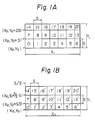
- Figs. 1A and 1B are diagrams of a rectangular area divided into a plurality of areas in accordance with the present invention;
- Fig. 2 is a block diagram illustrating an embodiment of the scanning electron-beam exposure system according to the present invention;
- Fig. 3 is a circuit diagram of the
pattern generator 203A of Fig. 2; and - Fig. 4 is a circuit diagram of the
pattern generator 203B of Fig. 2. - A rectangular pattern stored in a data memory (shown in Fig. 2 but not in Fig. 1) is determined by terminal coordinate information (Xo, Yo) and size (Xi, Yi). Here, if the maximum rectangle of an electron beam is defined as SxS, as is illustrated in Fig. 1A, the, rectangular pattern is divided into patterns 0
thorugh 6 arranged in the X direction of the coordinates (Xo, Yo),patterns 7 through 13 arranged in the X direction of the coordinates (Xo, Yo+S), andpatterns 14through 20 arranged in the X direction of the coordinates (Xo, Yo+2S). In this case, thepatterns - In an embodiment of the invention, such two kinds of divided patterns are prepared. First, the patterns 0 through 20, respectively, of Fig. 1A are exposed by half of a predetermined electron-beam dose. Next, the patterns 0' through 20', respectively, of Fig. 1B are exposed by half of the predetermined electron-beam dose. That is, an exposure operation is performed so as to superpose the exposed patterns of Fig. 1A on the exposed patterns of Fig. 1B. As a result, deviation of the border of each of the patterns 0
thorugh 20 and the patterns 0' through 20' is prevented. - In Fig. 2, which illustrates an embodiment of the present invention,
reference numeral 201 indicates a central processing unit (CPU), andreference numeral 202 indicates a data memory for storing rectangular patterns such as the rectangular pattern illustrated in Fig. 1A or Fig. 1B. That is, in this case, thedata memory 202 stores terminal coordinate information (X0, Yo) and size information (X1, Y,).Reference numerals pattern generator 203A generates terminal coordinate information (xo, yo) and size information (Sx, Sy) as parameters corresponding to each divided pattern illustrated in Fig. 1A to adriver circuit 204. Similarly, thepattern generator 203B generates parameters xo, yo, Sx, and Sy corresponding to each divided pattern illustrated in Fig. 1B to thedriver circuit 204. Thedriver circuit 204 drives amain deflection lens 205 and aslit deflection lens 206 to determine the beam positions xo and yo and the beam size Sx and Sy. A stage-driver control circuit 207 is used for moving a stage of the electron-beam exposure system. - The operation of the
pattern generator 203A is initiated by a start signal ST1 of theCPU 201 and proceeds with the pulses of a system clock signal CK1. When exposure of the divided patterns illustrated in Fig. 1A is completed, thepattern generator 203A generates an exposure end signal ED1 which is transmtited to theCPU 201. Next, theCPU 201 generates a start signal ST2 to initiate operation of thepattern generator 203B which proceeds with the pulses of a system clock signal CK2. When exposure of the divided patterns illustrated in Fig. 1 B is completed, thepattern generator 203B generates an exposure end signal ED2 which is trransmitted to theCPU 201. As a result, exposure of the rectangular patterns illustrated in Figs. 1A and 1B is completed. Therefore, theCPU 201 proceeds to expose the next rectangular pattern stored in thedata memory 202. - The
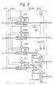
pattern generators - In Fig. 3, which illustrates the
pattern generator 203A of Fig. 2, aregister 301 and anadder 302 are provided in order to generate X-direction coordinate information xo of a terminal point of a divided pattern, and aregister 303 and anadder 304 are provided in order to generate Y-direction coordinate information yo of a terminal point of a divided pattern. In addition, aregister 305, asubtracter 306, acomparator 307, and aselector 308 are provided in order to generate size information Sx in the X-direction of a divided pattern, and aregister 309, asubtractor 310, acomparator 311, and aselector 312 are provided in order to generate size information Sy in the Y-direction of a divided pattern. - The operation of the circuit of Fig. 3 is explained with reference to Fig. 1A. First, the
CPU 201 generates a start signal ST1, and parameters Xo, Yo, X, and Y1, are supplied from thedata memory 202 to theregisters comparator 307 compares X1 with the maximum size S. As a result, since X,>S, theselector 308 selects the lower input S thereof and, accordingly, SX=S. In addition, thecomparator 311 compares Y, with the maximum size S. As a result, since Yi>S, theselector 312 selects the lower input S thereof and, accordingly, Sy=S. That is, pattern 0 of the parameters (xo, yo, Sx, Sy) in (Xo, Yo, S, S). - Next, after the
driver circuit 204 exposes the pattern 0 with a predetermined dose, theCPU 201 generates a pulse of the system clock signal CK1. As a result, thepattern generator 203A performs an operation for generating the pattern 1 of the parameters shown in Fig. 1A. That is, the value of theregister 301 is changed by theadder 302 from Xo to Xo+S. In addition, the value of theregister 305 is changed by the subtractor 306 from X1 to X,-S. In this case, the output of thecomparators 


- Similarly, the
pattern generator 203A performs, an operation for generating thepattern 6 of the parameters (xo, yo, Sx, Sy) shown in Fig. 1A so that thepattern 6 of the parameters is
comparator 307 changes so that theselector 308 selects the upper input thereof and the X-direction scanning and signal EX becomes logic "1". In this state, when the next pulse of the system clock signal CK1 is generated, a signal EX' becomes logic "1" so that Xo is again stored in theregister 301 and the value of theregister 303 is changed from Y0 to Yo+S. In addition, X1 is again stored in theregister 305 and the value of theregister 309 is changed from Y, to Y1-S. In this case, since X1-S<S and Y1-S<S, theselectors pattern 7 of the parameters (xo, yo, Sx, Sy) is
- Finally, the
pattern generator 203A performs an operation for generating thepattern 20 of the parameters (xo, yo, Sx, Sy) shown in Fig. 1A so that thepattern 20 of the parameters is
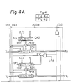
comparators CPU 201, thereby completing the exposure operation. - In Fig. 4, which illustrates the
pattern generator 203B of Fig. 2,selectors 401 through 404 are added to the elements of Fig. 3. That is, theselectors selectors comparators - The operation of the circuit of Fig. 4 is explained with reference to Fig. 1B. First, the
CPU 201 generates a start signal ST2, and parameters Xo, Yo, X1, and Y, are supplied from thedata memory 202 to theregisters selectors 401 through 404 select S/2. Therefore, thecomparator 307 compares X1 with S/2. As a result, since X1>S/2, theselector 308 selects the lower input S/2 thereof and, accordingly, Sx=S/2. In addition, thecomparator 311 compares Y1 with S/2. As a result, since Y1>S/2, theselector 312 selects the lower input S/2 thereof and, accordingly, Sy=S/2. That is, the pattern 0' of the parameters (xo, yo, Sx, Sy) is (Xo, Yo, S/2, S/2). - Next, after the
driver circuit 204 exposes the pattern 0' with a predetermined electron-beam dose, theCPU 201 generates a pulse of the system clock CK2 applied as a control signal toselectors adders pattern generator 203B performs an operation for generating the pattern 1' of the parameters shown in Fig. 1 B. That is, the value of theregister 301 is changed by theadder 302 from Xo to Xo+S/2. In addition, the value of theregister 305 is changed by the subtractor 306 from X1 to X1-S/2. That is,subtractor 306 is supplied with S/2 instead of S by not-shown selector means. In this case, the outputs of thecomparators selector 403 selects the value S (due to CK2). Therefore,


- Thus, the
pattern generator 203B performs an operation for generating the pattern 6' of the parameters (xo, yo, Sx, Sy) shown in Fig. 1B so that the pattern 6' of the parameters is
comparator 307 changes so that theselector 308 selects the upper input thereof and the X-direction scanning end signal EX becomes logic "1" and is applied as a control signal to theselectors registers adders register 301 and the value of theregister 303 is changed from Yo to Yo+S/2. In addition, X1 is again stored in theregister 305 and the value of theregister 309 is changed from Y1 to Y1-S/2. That is,subtractor 310 is supplied with S/2 instead of S by not-shown selector means. In this case, since X1-S>S and Y1-S/2>S, theselectors selectors 
- Finally, the
pattern generator 203B performs an operation for generating the pattern 20' of the parameters (xo, y0, Sx, Sy) shown in Fig. 1 B so that the pattern 20' of the parameters is
comparators CPU 201, thereby completing the exposure operation. - In the above-mentioned embodiment, the shift quantities in the X- and Y-directions between the two kinds of divided patterns are both S/2. However, it should be noted that such shift quantities can be other values only when both the X-direction and the Y-direction are shifted.
- As was explained above, in an embodiment of the present invention, deviation of the border of patterns can be protected against.
Claims (5)
Applications Claiming Priority (2)
| Application Number | Priority Date | Filing Date | Title |
|---|---|---|---|
| JP11153482A JPS593923A (en) | 1982-06-30 | 1982-06-30 | Electron beam exposing method |
| JP111534/82 | 1982-06-30 |
Publications (3)
| Publication Number | Publication Date |
|---|---|
| EP0098177A2 EP0098177A2 (en) | 1984-01-11 |
| EP0098177A3 EP0098177A3 (en) | 1986-06-04 |
| EP0098177B1 true EP0098177B1 (en) | 1989-03-22 |
Family
ID=14563780
Family Applications (1)
| Application Number | Title | Priority Date | Filing Date |
|---|---|---|---|
| EP19830303812 Expired EP0098177B1 (en) | 1982-06-30 | 1983-06-30 | Scanning electron-beam exposure system |
Country Status (3)
| Country | Link |
|---|---|
| EP (1) | EP0098177B1 (en) |
| JP (1) | JPS593923A (en) |
| DE (1) | DE3379487D1 (en) |
Families Citing this family (6)
| Publication number | Priority date | Publication date | Assignee | Title |
|---|---|---|---|---|
| US4818885A (en) * | 1987-06-30 | 1989-04-04 | International Business Machines Corporation | Electron beam writing method and system using large range deflection in combination with a continuously moving table |
| US4816692A (en) * | 1987-07-08 | 1989-03-28 | International Business Machines Corporation | Pattern splicing system and method for scanning of electron beam system |
| JPH01286310A (en) * | 1988-05-12 | 1989-11-17 | Nec Corp | Charged beam exposure method |
| EP0433993B1 (en) * | 1989-12-21 | 1997-03-19 | Fujitsu Limited | Method and apparatus for controlling charged particle beams in charged particle beam exposure system |
| US5393987A (en) * | 1993-05-28 | 1995-02-28 | Etec Systems, Inc. | Dose modulation and pixel deflection for raster scan lithography |
| US5624774A (en) * | 1994-06-16 | 1997-04-29 | Nikon Corporation | Method for transferring patterns with charged particle beam |
Family Cites Families (4)
| Publication number | Priority date | Publication date | Assignee | Title |
|---|---|---|---|---|
| US4099062A (en) * | 1976-12-27 | 1978-07-04 | International Business Machines Corporation | Electron beam lithography process |
| JPS5493364A (en) * | 1977-12-30 | 1979-07-24 | Fujitsu Ltd | Exposure system for electron beam |
| JPS5831728B2 (en) * | 1979-12-04 | 1983-07-08 | 日本電子株式会社 | Electron beam exposure method |
| EP0053225B1 (en) * | 1980-11-28 | 1985-03-13 | International Business Machines Corporation | Electron beam system and method |
-
1982
- 1982-06-30 JP JP11153482A patent/JPS593923A/en active Granted
-
1983
- 1983-06-30 DE DE8383303812T patent/DE3379487D1/en not_active Expired
- 1983-06-30 EP EP19830303812 patent/EP0098177B1/en not_active Expired
Also Published As
| Publication number | Publication date |
|---|---|
| JPS593923A (en) | 1984-01-10 |
| EP0098177A3 (en) | 1986-06-04 |
| EP0098177A2 (en) | 1984-01-11 |
| JPH0341974B2 (en) | 1991-06-25 |
| DE3379487D1 (en) | 1989-04-27 |
Similar Documents
| Publication | Publication Date | Title |
|---|---|---|
| US7772575B2 (en) | Stencil design and method for cell projection particle beam lithography | |
| JP3206143B2 (en) | Charged particle beam exposure method | |
| JPH07191199A (en) | Method and system for exposure with charged particle beam | |
| KR19980080256A (en) | Charged particle beam exposure method and method of forming pattern on wafer | |
| KR100581478B1 (en) | Method and apparatus for direct writing of semiconductor die using microcolumn array | |
| JP2002118060A (en) | Charged particle beam projection aligner, charged particle beam exposure method, exposure data creation method, computer-readable recording medium with program for creating exposure data stored, and computer with exposure data stored therein | |
| EP1060498A1 (en) | A method and apparatus that determines charged particle beam shape codes | |
| KR100253052B1 (en) | Method for forming a pattern and apparatus for forming a pattern | |
| US5968686A (en) | Charged-beam exposure mask and charged-beam exposure method | |
| EP1060500B1 (en) | An apparatus and method for controlling a beam shape in lithographiy systems | |
| EP0098177B1 (en) | Scanning electron-beam exposure system | |
| JP2835140B2 (en) | Blanking aperture array, manufacturing method thereof, charged particle beam exposure apparatus, and charged particle beam exposure method | |
| US20060289797A1 (en) | Electron beam writing method, electron beam writing apparatus and semiconductor device manufacturing method | |
| US6352802B1 (en) | Mask for electron beam exposure and method of manufacturing semiconductor device using the same | |
| US6182369B1 (en) | Pattern forming apparatus | |
| US7041991B2 (en) | Variably shaped beam EB writing system | |
| JP2874688B2 (en) | Mask and electron beam exposure method using the same | |
| JPH04252016A (en) | Pattern drawing method | |
| US6444399B1 (en) | Methods for achieving reduced effects of overlayer and subfield-stitching errors in charged-particle-beam microlithography, and device manufacturing methods comprising such microlithography methods | |
| JP3206448B2 (en) | Electron beam lithography system | |
| JPH0669112A (en) | Transparent mask plate | |
| JPH0536594A (en) | Exposure treatment system, charged particle beam aligner and charged particle beam exposure method | |
| JP3481017B2 (en) | Charged particle beam exposure apparatus and exposure data processing method of the charged particle beam exposure apparatus | |
| JP2992081B2 (en) | Pattern creation device | |
| JP2871617B2 (en) | Electron beam exposure method |
Legal Events
| Date | Code | Title | Description |
|---|---|---|---|
| PUAI | Public reference made under article 153(3) epc to a published international application that has entered the european phase |
Free format text: ORIGINAL CODE: 0009012 |
|
| AK | Designated contracting states |
Designated state(s): DE FR GB |
|
| PUAL | Search report despatched |
Free format text: ORIGINAL CODE: 0009013 |
|
| AK | Designated contracting states |
Kind code of ref document: A3 Designated state(s): DE FR GB |
|
| 17P | Request for examination filed |
Effective date: 19860624 |
|
| 17Q | First examination report despatched |
Effective date: 19870810 |
|
| GRAA | (expected) grant |
Free format text: ORIGINAL CODE: 0009210 |
|
| AK | Designated contracting states |
Kind code of ref document: B1 Designated state(s): DE FR GB |
|
| REF | Corresponds to: |
Ref document number: 3379487 Country of ref document: DE Date of ref document: 19890427 |
|
| ET | Fr: translation filed | ||
| PLBE | No opposition filed within time limit |
Free format text: ORIGINAL CODE: 0009261 |
|
| STAA | Information on the status of an ep patent application or granted ep patent |
Free format text: STATUS: NO OPPOSITION FILED WITHIN TIME LIMIT |
|
| 26N | No opposition filed | ||
| PGFP | Annual fee paid to national office [announced via postgrant information from national office to epo] |
Ref country code: FR Payment date: 19960611 Year of fee payment: 14 |
|
| PGFP | Annual fee paid to national office [announced via postgrant information from national office to epo] |
Ref country code: GB Payment date: 19960621 Year of fee payment: 14 |
|
| PGFP | Annual fee paid to national office [announced via postgrant information from national office to epo] |
Ref country code: DE Payment date: 19960627 Year of fee payment: 14 |
|
| PG25 | Lapsed in a contracting state [announced via postgrant information from national office to epo] |
Ref country code: GB Free format text: LAPSE BECAUSE OF NON-PAYMENT OF DUE FEES Effective date: 19970630 |
|
| GBPC | Gb: european patent ceased through non-payment of renewal fee |
Effective date: 19970630 |
|
| PG25 | Lapsed in a contracting state [announced via postgrant information from national office to epo] |
Ref country code: FR Free format text: LAPSE BECAUSE OF NON-PAYMENT OF DUE FEES Effective date: 19980227 |
|
| PG25 | Lapsed in a contracting state [announced via postgrant information from national office to epo] |
Ref country code: DE Free format text: LAPSE BECAUSE OF NON-PAYMENT OF DUE FEES Effective date: 19980303 |
|
| REG | Reference to a national code |
Ref country code: FR Ref legal event code: ST |
|
| REG | Reference to a national code |
Ref country code: FR Ref legal event code: ST |