EP0095094A2 - Photomaske mit korrigiertem Weissfehler - Google Patents
Photomaske mit korrigiertem Weissfehler Download PDFInfo
- Publication number
- EP0095094A2 EP0095094A2 EP83104651A EP83104651A EP0095094A2 EP 0095094 A2 EP0095094 A2 EP 0095094A2 EP 83104651 A EP83104651 A EP 83104651A EP 83104651 A EP83104651 A EP 83104651A EP 0095094 A2 EP0095094 A2 EP 0095094A2
- Authority
- EP
- European Patent Office
- Prior art keywords
- acid
- photomask
- white defects
- silver
- film
- Prior art date
- Legal status (The legal status is an assumption and is not a legal conclusion. Google has not performed a legal analysis and makes no representation as to the accuracy of the status listed.)
- Withdrawn
Links
Images
Classifications
-
- G—PHYSICS
- G03—PHOTOGRAPHY; CINEMATOGRAPHY; ANALOGOUS TECHNIQUES USING WAVES OTHER THAN OPTICAL WAVES; ELECTROGRAPHY; HOLOGRAPHY
- G03F—PHOTOMECHANICAL PRODUCTION OF TEXTURED OR PATTERNED SURFACES, e.g. FOR PRINTING, FOR PROCESSING OF SEMICONDUCTOR DEVICES; MATERIALS THEREFOR; ORIGINALS THEREFOR; APPARATUS SPECIALLY ADAPTED THEREFOR
- G03F1/00—Originals for photomechanical production of textured or patterned surfaces, e.g., masks, photo-masks, reticles; Mask blanks or pellicles therefor; Containers specially adapted therefor; Preparation thereof
- G03F1/68—Preparation processes not covered by groups G03F1/20 - G03F1/50
- G03F1/72—Repair or correction of mask defects
-
- G—PHYSICS
- G03—PHOTOGRAPHY; CINEMATOGRAPHY; ANALOGOUS TECHNIQUES USING WAVES OTHER THAN OPTICAL WAVES; ELECTROGRAPHY; HOLOGRAPHY
- G03F—PHOTOMECHANICAL PRODUCTION OF TEXTURED OR PATTERNED SURFACES, e.g. FOR PRINTING, FOR PROCESSING OF SEMICONDUCTOR DEVICES; MATERIALS THEREFOR; ORIGINALS THEREFOR; APPARATUS SPECIALLY ADAPTED THEREFOR
- G03F1/00—Originals for photomechanical production of textured or patterned surfaces, e.g., masks, photo-masks, reticles; Mask blanks or pellicles therefor; Containers specially adapted therefor; Preparation thereof
- G03F1/54—Absorbers, e.g. of opaque materials
-
- Y—GENERAL TAGGING OF NEW TECHNOLOGICAL DEVELOPMENTS; GENERAL TAGGING OF CROSS-SECTIONAL TECHNOLOGIES SPANNING OVER SEVERAL SECTIONS OF THE IPC; TECHNICAL SUBJECTS COVERED BY FORMER USPC CROSS-REFERENCE ART COLLECTIONS [XRACs] AND DIGESTS
- Y10—TECHNICAL SUBJECTS COVERED BY FORMER USPC
- Y10S—TECHNICAL SUBJECTS COVERED BY FORMER USPC CROSS-REFERENCE ART COLLECTIONS [XRACs] AND DIGESTS
- Y10S430/00—Radiation imagery chemistry: process, composition, or product thereof
- Y10S430/139—Defect coating
-
- Y—GENERAL TAGGING OF NEW TECHNOLOGICAL DEVELOPMENTS; GENERAL TAGGING OF CROSS-SECTIONAL TECHNOLOGIES SPANNING OVER SEVERAL SECTIONS OF THE IPC; TECHNICAL SUBJECTS COVERED BY FORMER USPC CROSS-REFERENCE ART COLLECTIONS [XRACs] AND DIGESTS
- Y10—TECHNICAL SUBJECTS COVERED BY FORMER USPC
- Y10S—TECHNICAL SUBJECTS COVERED BY FORMER USPC CROSS-REFERENCE ART COLLECTIONS [XRACs] AND DIGESTS
- Y10S430/00—Radiation imagery chemistry: process, composition, or product thereof
- Y10S430/146—Laser beam
Definitions
- the present invention relates to a photomask used in the production of LSI's and other integrated circuits, and in particular to a photomask with corrected white defects.
- This film has a poor resistance to chemicals.
- the photomask is washed with acid or alkali to remove attached dust and other foreign matter prior to use, the silver and titanium oxide are dissolved.
- the object of the present invention is to provide a photomask with white defects that have been corrected with a film having excellent resistance to chemicals.
- This object is achieved by applying a composition comprising silver nitrate, at least one compound selected from the group of tantalum complexes described by general formulas (1) to (3) (wherein R 1 , R 3 and R 5 are alkyl groups of 1 to 18 carbon atoms, R 2 and R 4 are alkyl or alkoxy groups of 1 to 18 carbon atoms, and 1, m, n, and k are 0 or integers from 1 to 5, with n + k ⁇ 5), and a solvent to at least the white defects on the photomask, and training a laser beam locally onto the defects to cause the deposition of silver and tantalum oxide such as to form a mixed deposition film.
- the materials employed in the present invention are described below. Irradiation of the silver nitrate by the laser beam causes a photochemical reaction to occur. The heat generated by absorption of the beam produces silver, which imparts light-shielding properties to the deposited film. The use of silver nitrate also provides excellent sensitivity and resolution.
- the tantalum complexes represented by formulas (1) to (3) above undergo thermal decomposition under the effects of the heat generated by absorption of the laser light, giving tantalum oxide, which is present between the silver particles in the deposited film. This enhances the strength of the deposited film, its adhesion to the photomask pattern, and its resistance to chemicals, as a result of which the film does not dissolve during washing of the photomask.
- Use of the tantalum complexes also enables the formation of a uniform film.
- the strength of the deposited film, and its adhesion to the photomask substrate and the photomask pattern become inadequate.
- a molar ratio of more than 5 provides only a small content of the light-shielding component silver in the deposited film, resulting in inadequate light-shielding properties.
- the solvents in the invention should preferably be mixtures of the nitrile substitution product of an aliphatic hydrocarbon, such as acetonitrile or propionitrile, and either an alcohol such as methanol, ethanol, or isopropanol, or the monoalkyl ethers of ethylene glycol, such as ethylene glycol monomethyl ether or ethylene glycol monoethyl ether.
- an aliphatic hydrocarbon such as acetonitrile or propionitrile
- an alcohol such as methanol, ethanol, or isopropanol
- the monoalkyl ethers of ethylene glycol such as ethylene glycol monomethyl ether or ethylene glycol monoethyl ether.
- a carboxylic acid in the above composition, which comprises silver nitrate, at least one compound selected from the group of tantalum complexes described by formulas (1) to (3), and a solvent, further enhances the strength of the deposited film and its adhesion both to the photomask substrate and the photomask pattern.
- a carboxylic acid reduces the particle size of the silver grains in the tantalum oxide.
- a polybasic carboxylic acid is desirable as the carboxylic acid.
- This may be, for example, malonic acid, methylmalonic acid, succinic acid, methylsuccinic acid, glutaric acid, adipic acid, suberic acid, azelaic acid, sebacic acid, itaconic acid, maleic acid, citraconic acid, ethylmaleic acid, or mesaconic acid.
- These acids may be used alone or in a mixture of two or more thereof.
- the mixing ratio in moles of the silver nitrate and carboxylic acid in the composition should preferably fall within the range given in Eq. (II).
- composition used in the present invention can be applied by spin coating to give a uniform film. Brush coating and dipping are also suitable for application.
- a beam of condensed light may be used to irradiate the desired portions of the film, but a laser beam is preferable.
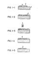
- Figs. 1-1 to 1-5 are schematic views showing the process of correcting a white defect in a photomask.
- Composition Nos. 1 to 14 in the table were spin coated at 2000 rpm on the white defect 3 in the chromium pattern 2 formed on the photomask substsrate ( F ig. 1-1) and dried for 5 minutes at 80°C to form film 4 shown in Fig. 1-2.
- the defect was selectively irradiated for 60 seconds with an argon laser beam, causing the deposition of silver and tantalum oxide to form a light-shielding mixed deposition film (Fig. 1-4).
- the area irradiated with laser light was a 10-micron square on the substrate surface, and the power at the irradiated surface was 3000 W/cm.
- the thickness, transmission ratio of 488-mm wavelength, light, and adhesion to the substrate of the deposited film are given in the table.
- the symbol 0 stands for good, and the symbol for excellent.
- composition in the present invention provides a deposited film that is sufficiently light-shielding and has good adhesion to the substrate.
- the table also shows that compositions containing a carboxylic acid have excellent adhesion to the substrate.
- the alkali resistance was determined by measuring the light transmission ratio after 30 minutes of immersion in an aqueous solution of 5% NaOH at 50°C, and comparing this with the initial value.
- the resistance to acid was determined by measuring the transmission ratio after 30 minutes of immersion in hot, concentrated sulfuric acid at 100°C, and comparing this with the initial value.
- the respective test values are given in the table.
- the deposited film had a thickness of 1500 A and a transmission ratio for 488-mm wavelength light of 3%. Adhesion of the film to the photomask substrate was excellent.
Landscapes
- Physics & Mathematics (AREA)
- General Physics & Mathematics (AREA)
- Preparing Plates And Mask In Photomechanical Process (AREA)
- Paints Or Removers (AREA)
- Inks, Pencil-Leads, Or Crayons (AREA)
- Inorganic Compounds Of Heavy Metals (AREA)
Applications Claiming Priority (2)
| Application Number | Priority Date | Filing Date | Title |
|---|---|---|---|
| JP57086604A JPS58203443A (ja) | 1982-05-24 | 1982-05-24 | ホトマスクの白点欠陥修正用組成物 |
| JP86604/82 | 1982-05-24 |
Publications (2)
| Publication Number | Publication Date |
|---|---|
| EP0095094A2 true EP0095094A2 (de) | 1983-11-30 |
| EP0095094A3 EP0095094A3 (de) | 1984-10-03 |
Family
ID=13891613
Family Applications (1)
| Application Number | Title | Priority Date | Filing Date |
|---|---|---|---|
| EP83104651A Withdrawn EP0095094A3 (de) | 1982-05-24 | 1983-05-11 | Photomaske mit korrigiertem Weissfehler |
Country Status (3)
| Country | Link |
|---|---|
| US (1) | US4510222A (de) |
| EP (1) | EP0095094A3 (de) |
| JP (1) | JPS58203443A (de) |
Cited By (2)
| Publication number | Priority date | Publication date | Assignee | Title |
|---|---|---|---|---|
| WO1995026355A1 (en) * | 1994-03-26 | 1995-10-05 | Timothy John Leedham | Tantalum compounds |
| WO1996008587A1 (en) * | 1994-09-16 | 1996-03-21 | Advanced Technology Materials, Inc. | Tantalum and niobium reagents useful in chemical vapor deposition processes, and process for depositing coatings using the same |
Families Citing this family (31)
| Publication number | Priority date | Publication date | Assignee | Title |
|---|---|---|---|---|
| JPS60196942A (ja) * | 1984-03-21 | 1985-10-05 | Hitachi Ltd | フオトマスク欠陥修正方法 |
| US4592975A (en) * | 1984-06-20 | 1986-06-03 | Gould Inc. | Method for repairing a photomask by laser-induced polymer degradation |
| US4636403A (en) * | 1985-04-29 | 1987-01-13 | At&T Technologies, Inc. | Method of repairing a defective photomask |
| NL8802047A (nl) * | 1988-08-18 | 1990-03-16 | Philips Nv | Werkwijze voor het selectief op een substraat aanbrengen van een metaal uit de vloeistoffase met behulp van een laser. |
| US6110529A (en) * | 1990-07-06 | 2000-08-29 | Advanced Tech Materials | Method of forming metal films on a substrate by chemical vapor deposition |
| US7323581B1 (en) | 1990-07-06 | 2008-01-29 | Advanced Technology Materials, Inc. | Source reagent compositions and method for forming metal films on a substrate by chemical vapor deposition |
| US5840897A (en) * | 1990-07-06 | 1998-11-24 | Advanced Technology Materials, Inc. | Metal complex source reagents for chemical vapor deposition |
| US5820664A (en) * | 1990-07-06 | 1998-10-13 | Advanced Technology Materials, Inc. | Precursor compositions for chemical vapor deposition, and ligand exchange resistant metal-organic precursor solutions comprising same |
| US5164565A (en) * | 1991-04-18 | 1992-11-17 | Photon Dynamics, Inc. | Laser-based system for material deposition and removal |
| US5175504A (en) * | 1991-06-17 | 1992-12-29 | Photon Dynamics, Inc. | Method and apparatus for automatically inspecting and repairing a simple matrix circuit panel |
| US5235272A (en) * | 1991-06-17 | 1993-08-10 | Photon Dynamics, Inc. | Method and apparatus for automatically inspecting and repairing an active matrix LCD panel |
| US5432461A (en) * | 1991-06-28 | 1995-07-11 | Photon Dynamics, Inc. | Method of testing active matrix liquid crystal display substrates |
| US5459409A (en) * | 1991-09-10 | 1995-10-17 | Photon Dynamics, Inc. | Testing device for liquid crystal display base plate |
| US5444385A (en) * | 1991-09-10 | 1995-08-22 | Photon Dynamics, Inc. | Testing apparatus for liquid crystal display substrates |
| US5504438A (en) * | 1991-09-10 | 1996-04-02 | Photon Dynamics, Inc. | Testing method for imaging defects in a liquid crystal display substrate |
| US5465052A (en) * | 1991-09-10 | 1995-11-07 | Photon Dynamics, Inc. | Method of testing liquid crystal display substrates |
| US5543729A (en) * | 1991-09-10 | 1996-08-06 | Photon Dynamics, Inc. | Testing apparatus and connector for liquid crystal display substrates |
| US5916359A (en) * | 1995-03-31 | 1999-06-29 | Advanced Technology Materials, Inc. | Alkane and polyamine solvent compositions for liquid delivery chemical vapor deposition |
| US6133051A (en) * | 1998-06-30 | 2000-10-17 | Advanced Technology Materials, Inc. | Amorphously deposited metal oxide ceramic films |
| US6015917A (en) | 1998-01-23 | 2000-01-18 | Advanced Technology Materials, Inc. | Tantalum amide precursors for deposition of tantalum nitride on a substrate |
| US7012292B1 (en) * | 1998-11-25 | 2006-03-14 | Advanced Technology Materials, Inc | Oxidative top electrode deposition process, and microelectronic device structure |
| US6261723B1 (en) | 1999-03-04 | 2001-07-17 | International Business Machines Corporation | Transfer layer repair process for attenuated masks |
| US7084080B2 (en) * | 2001-03-30 | 2006-08-01 | Advanced Technology Materials, Inc. | Silicon source reagent compositions, and method of making and using same for microelectronic device structure |
| US20030221748A1 (en) * | 2002-05-30 | 2003-12-04 | Fry's Metals, Inc. | Solder paste flux system |
| US6960675B2 (en) * | 2003-10-14 | 2005-11-01 | Advanced Technology Materials, Inc. | Tantalum amide complexes for depositing tantalum-containing films, and method of making same |
| US7166732B2 (en) * | 2004-06-16 | 2007-01-23 | Advanced Technology Materials, Inc. | Copper (I) compounds useful as deposition precursors of copper thin films |
| US20060102895A1 (en) * | 2004-11-16 | 2006-05-18 | Hendrix Bryan C | Precursor compositions for forming tantalum-containing films, and tantalum-containing barrier films and copper-metallized semiconductor device structures |
| US9312557B2 (en) * | 2005-05-11 | 2016-04-12 | Schlumberger Technology Corporation | Fuel cell apparatus and method for downhole power systems |
| TW200825200A (en) * | 2006-12-05 | 2008-06-16 | Advanced Tech Materials | Metal aminotroponiminates, bis-oxazolinates and guanidinates |
| US7750173B2 (en) * | 2007-01-18 | 2010-07-06 | Advanced Technology Materials, Inc. | Tantalum amido-complexes with chelate ligands useful for CVD and ALD of TaN and Ta205 thin films |
| CN109390217B (zh) * | 2017-08-09 | 2020-09-25 | 华邦电子股份有限公司 | 光掩膜及半导体装置的形成方法 |
Family Cites Families (7)
| Publication number | Priority date | Publication date | Assignee | Title |
|---|---|---|---|---|
| GB1461176A (en) * | 1974-04-11 | 1977-01-13 | Plessey Inc | Method of producing powdered materials |
| EP0054068A1 (de) * | 1980-06-19 | 1982-06-23 | Master Images Inc. | Verfahren zum bilden einer tadellosen photomaske oder zum ausbessern einer bestehenden photomaske, und erzeugnis derselben |
| US4340654A (en) * | 1980-06-19 | 1982-07-20 | Campi James G | Defect-free photomask |
| US4444801A (en) * | 1981-01-14 | 1984-04-24 | Hitachi, Ltd. | Method and apparatus for correcting transparent defects on a photomask |
| JPS57206026A (en) * | 1981-06-12 | 1982-12-17 | Hitachi Ltd | Defect correcting method of photomask |
| JPS586128A (ja) * | 1981-07-03 | 1983-01-13 | Hitachi Ltd | フォトマスクの欠落欠陥修正装置 |
| JPS586127A (ja) * | 1981-07-03 | 1983-01-13 | Hitachi Ltd | フオトマスク欠陥修正方法とその装置 |
-
1982
- 1982-05-24 JP JP57086604A patent/JPS58203443A/ja active Granted
-
1983
- 1983-05-11 EP EP83104651A patent/EP0095094A3/de not_active Withdrawn
- 1983-05-19 US US06/496,245 patent/US4510222A/en not_active Expired - Fee Related
Cited By (2)
| Publication number | Priority date | Publication date | Assignee | Title |
|---|---|---|---|---|
| WO1995026355A1 (en) * | 1994-03-26 | 1995-10-05 | Timothy John Leedham | Tantalum compounds |
| WO1996008587A1 (en) * | 1994-09-16 | 1996-03-21 | Advanced Technology Materials, Inc. | Tantalum and niobium reagents useful in chemical vapor deposition processes, and process for depositing coatings using the same |
Also Published As
| Publication number | Publication date |
|---|---|
| US4510222A (en) | 1985-04-09 |
| JPS58203443A (ja) | 1983-11-26 |
| EP0095094A3 (de) | 1984-10-03 |
| JPS6228462B2 (de) | 1987-06-20 |
Similar Documents
| Publication | Publication Date | Title |
|---|---|---|
| EP0095094A2 (de) | Photomaske mit korrigiertem Weissfehler | |
| DE69704294T2 (de) | Positiv arbeitende, fotoempfindliche Harzzusammensetzung und Halbleiteranordnung mit dieser Zusammensetzung | |
| DE2733267C2 (de) | Photolack | |
| EP0164083A2 (de) | Positiv arbeitende strahlungsempfindliche Beschichtungslösung | |
| JPS606961B2 (ja) | 光重合性被着組成物及びその被着方法 | |
| DE2312499A1 (de) | Diazochinon-siloxane und verwendung derselben fuer photolacke und lichtempfindliche gegenstaende | |
| EP0710522B1 (de) | Flussmittelzusammensetzung | |
| JPH03184695A (ja) | フラックス及びはんだペースト用添加剤 | |
| JPH0592296A (ja) | フラツクス又ははんだペースト用腐食防止剤 | |
| JPH03252500A (ja) | フラックス洗浄剤 | |
| JPH0388386A (ja) | プリント基板アセンブリの製造 | |
| DE69729562T2 (de) | Decafluorpentanzusammensetzungen | |
| JPH03106594A (ja) | ハンダ付け用フラックス組成物 | |
| US3684569A (en) | Process of producing conductive gold patterns | |
| JPS5821329A (ja) | フオトマスクの白点欠陥修正用組成物 | |
| US3281222A (en) | Activated rosin fluxes and cored solders made therefrom | |
| US3366481A (en) | Photoengraving resists and compositions therefor | |
| DE69012941T2 (de) | Verfahren und material zum schützen und zum verbessern der lötbarkeit von metallischen oberflächen. | |
| US2739892A (en) | Light-sensitive photomechanical resist compositions | |
| JPH06500051A (ja) | 光により発生される酸化物除去剤を有する半田付け用フラックス | |
| JPS6129895B2 (de) | ||
| CH643865A5 (de) | Zusammensetzung, enthaltend ein komplexsalz in esterloesung. | |
| JPS6351470B2 (de) | ||
| JPS61258242A (ja) | 感光性組成物及びそれを用いたパタ−ン形成方法 | |
| FR2475753A1 (fr) | Plaque lithographique a base de fluoborate de paradiazodiphenylamine et de resine epoxy liquide |
Legal Events
| Date | Code | Title | Description |
|---|---|---|---|
| PUAI | Public reference made under article 153(3) epc to a published international application that has entered the european phase |
Free format text: ORIGINAL CODE: 0009012 |
|
| 17P | Request for examination filed |
Effective date: 19830609 |
|
| AK | Designated contracting states |
Designated state(s): DE GB |
|
| PUAL | Search report despatched |
Free format text: ORIGINAL CODE: 0009013 |
|
| AK | Designated contracting states |
Designated state(s): DE GB |
|
| 17Q | First examination report despatched |
Effective date: 19860714 |
|
| STAA | Information on the status of an ep patent application or granted ep patent |
Free format text: STATUS: THE APPLICATION HAS BEEN WITHDRAWN |
|
| 18W | Application withdrawn |
Withdrawal date: 19861027 |
|
| RIN1 | Information on inventor provided before grant (corrected) |
Inventor name: HONGO, MIKIO Inventor name: MIZUKOSHI, KATSURO Inventor name: OKUNAKA, MASAAKI Inventor name: MIYAUCHI, TATEOKI |