EP0090608A2 - Dispositif semi-conducteur à empaquetage moulé - Google Patents
Dispositif semi-conducteur à empaquetage moulé Download PDFInfo
- Publication number
- EP0090608A2 EP0090608A2 EP83301667A EP83301667A EP0090608A2 EP 0090608 A2 EP0090608 A2 EP 0090608A2 EP 83301667 A EP83301667 A EP 83301667A EP 83301667 A EP83301667 A EP 83301667A EP 0090608 A2 EP0090608 A2 EP 0090608A2
- Authority
- EP
- European Patent Office
- Prior art keywords
- leads
- main body
- semiconductor device
- package
- external leads
- Prior art date
- Legal status (The legal status is an assumption and is not a legal conclusion. Google has not performed a legal analysis and makes no representation as to the accuracy of the status listed.)
- Granted
Links
Images


Classifications
-
- H—ELECTRICITY
- H05—ELECTRIC TECHNIQUES NOT OTHERWISE PROVIDED FOR
- H05K—PRINTED CIRCUITS; CASINGS OR CONSTRUCTIONAL DETAILS OF ELECTRIC APPARATUS; MANUFACTURE OF ASSEMBLAGES OF ELECTRICAL COMPONENTS
- H05K3/00—Apparatus or processes for manufacturing printed circuits
- H05K3/30—Assembling printed circuits with electric components, e.g. with resistor
- H05K3/32—Assembling printed circuits with electric components, e.g. with resistor electrically connecting electric components or wires to printed circuits
- H05K3/34—Assembling printed circuits with electric components, e.g. with resistor electrically connecting electric components or wires to printed circuits by soldering
- H05K3/341—Surface mounted components
- H05K3/3421—Leaded components
- H05K3/3426—Leaded components characterised by the leads
-
- H—ELECTRICITY
- H01—ELECTRIC ELEMENTS
- H01L—SEMICONDUCTOR DEVICES NOT COVERED BY CLASS H10
- H01L23/00—Details of semiconductor or other solid state devices
- H01L23/28—Encapsulations, e.g. encapsulating layers, coatings, e.g. for protection
- H01L23/31—Encapsulations, e.g. encapsulating layers, coatings, e.g. for protection characterised by the arrangement or shape
- H01L23/3107—Encapsulations, e.g. encapsulating layers, coatings, e.g. for protection characterised by the arrangement or shape the device being completely enclosed
-
- H—ELECTRICITY
- H01—ELECTRIC ELEMENTS
- H01L—SEMICONDUCTOR DEVICES NOT COVERED BY CLASS H10
- H01L23/00—Details of semiconductor or other solid state devices
- H01L23/48—Arrangements for conducting electric current to or from the solid state body in operation, e.g. leads, terminal arrangements ; Selection of materials therefor
- H01L23/488—Arrangements for conducting electric current to or from the solid state body in operation, e.g. leads, terminal arrangements ; Selection of materials therefor consisting of soldered or bonded constructions
- H01L23/495—Lead-frames or other flat leads
- H01L23/49541—Geometry of the lead-frame
- H01L23/49548—Cross section geometry
- H01L23/49551—Cross section geometry characterised by bent parts
- H01L23/49555—Cross section geometry characterised by bent parts the bent parts being the outer leads
-
- H—ELECTRICITY
- H01—ELECTRIC ELEMENTS
- H01L—SEMICONDUCTOR DEVICES NOT COVERED BY CLASS H10
- H01L2224/00—Indexing scheme for arrangements for connecting or disconnecting semiconductor or solid-state bodies and methods related thereto as covered by H01L24/00
- H01L2224/01—Means for bonding being attached to, or being formed on, the surface to be connected, e.g. chip-to-package, die-attach, "first-level" interconnects; Manufacturing methods related thereto
- H01L2224/42—Wire connectors; Manufacturing methods related thereto
- H01L2224/47—Structure, shape, material or disposition of the wire connectors after the connecting process
- H01L2224/48—Structure, shape, material or disposition of the wire connectors after the connecting process of an individual wire connector
- H01L2224/4805—Shape
- H01L2224/4809—Loop shape
- H01L2224/48091—Arched
-
- H—ELECTRICITY
- H01—ELECTRIC ELEMENTS
- H01L—SEMICONDUCTOR DEVICES NOT COVERED BY CLASS H10
- H01L2224/00—Indexing scheme for arrangements for connecting or disconnecting semiconductor or solid-state bodies and methods related thereto as covered by H01L24/00
- H01L2224/01—Means for bonding being attached to, or being formed on, the surface to be connected, e.g. chip-to-package, die-attach, "first-level" interconnects; Manufacturing methods related thereto
- H01L2224/42—Wire connectors; Manufacturing methods related thereto
- H01L2224/47—Structure, shape, material or disposition of the wire connectors after the connecting process
- H01L2224/48—Structure, shape, material or disposition of the wire connectors after the connecting process of an individual wire connector
- H01L2224/481—Disposition
- H01L2224/48151—Connecting between a semiconductor or solid-state body and an item not being a semiconductor or solid-state body, e.g. chip-to-substrate, chip-to-passive
- H01L2224/48221—Connecting between a semiconductor or solid-state body and an item not being a semiconductor or solid-state body, e.g. chip-to-substrate, chip-to-passive the body and the item being stacked
- H01L2224/48245—Connecting between a semiconductor or solid-state body and an item not being a semiconductor or solid-state body, e.g. chip-to-substrate, chip-to-passive the body and the item being stacked the item being metallic
- H01L2224/48247—Connecting between a semiconductor or solid-state body and an item not being a semiconductor or solid-state body, e.g. chip-to-substrate, chip-to-passive the body and the item being stacked the item being metallic connecting the wire to a bond pad of the item
-
- H—ELECTRICITY
- H01—ELECTRIC ELEMENTS
- H01L—SEMICONDUCTOR DEVICES NOT COVERED BY CLASS H10
- H01L24/00—Arrangements for connecting or disconnecting semiconductor or solid-state bodies; Methods or apparatus related thereto
- H01L24/01—Means for bonding being attached to, or being formed on, the surface to be connected, e.g. chip-to-package, die-attach, "first-level" interconnects; Manufacturing methods related thereto
- H01L24/42—Wire connectors; Manufacturing methods related thereto
- H01L24/47—Structure, shape, material or disposition of the wire connectors after the connecting process
- H01L24/48—Structure, shape, material or disposition of the wire connectors after the connecting process of an individual wire connector
-
- H—ELECTRICITY
- H01—ELECTRIC ELEMENTS
- H01L—SEMICONDUCTOR DEVICES NOT COVERED BY CLASS H10
- H01L2924/00—Indexing scheme for arrangements or methods for connecting or disconnecting semiconductor or solid-state bodies as covered by H01L24/00
- H01L2924/0001—Technical content checked by a classifier
- H01L2924/00014—Technical content checked by a classifier the subject-matter covered by the group, the symbol of which is combined with the symbol of this group, being disclosed without further technical details
-
- H—ELECTRICITY
- H01—ELECTRIC ELEMENTS
- H01L—SEMICONDUCTOR DEVICES NOT COVERED BY CLASS H10
- H01L2924/00—Indexing scheme for arrangements or methods for connecting or disconnecting semiconductor or solid-state bodies as covered by H01L24/00
- H01L2924/10—Details of semiconductor or other solid state devices to be connected
- H01L2924/11—Device type
- H01L2924/14—Integrated circuits
-
- H—ELECTRICITY
- H01—ELECTRIC ELEMENTS
- H01L—SEMICONDUCTOR DEVICES NOT COVERED BY CLASS H10
- H01L2924/00—Indexing scheme for arrangements or methods for connecting or disconnecting semiconductor or solid-state bodies as covered by H01L24/00
- H01L2924/15—Details of package parts other than the semiconductor or other solid state devices to be connected
- H01L2924/181—Encapsulation
- H01L2924/1815—Shape
-
- Y—GENERAL TAGGING OF NEW TECHNOLOGICAL DEVELOPMENTS; GENERAL TAGGING OF CROSS-SECTIONAL TECHNOLOGIES SPANNING OVER SEVERAL SECTIONS OF THE IPC; TECHNICAL SUBJECTS COVERED BY FORMER USPC CROSS-REFERENCE ART COLLECTIONS [XRACs] AND DIGESTS
- Y02—TECHNOLOGIES OR APPLICATIONS FOR MITIGATION OR ADAPTATION AGAINST CLIMATE CHANGE
- Y02P—CLIMATE CHANGE MITIGATION TECHNOLOGIES IN THE PRODUCTION OR PROCESSING OF GOODS
- Y02P70/00—Climate change mitigation technologies in the production process for final industrial or consumer products
- Y02P70/50—Manufacturing or production processes characterised by the final manufactured product
Definitions
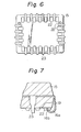
- FIG. 2 is a side view of
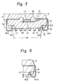
- Fig. 3 is a sectional view of
- Fig. 4 is a plan view of an embodiment of the present invention.
- the same portions are denoted by the same reference numerals.
- the tips 16b of the external leads 16 are formed perpendicular to or aslant (explained later) the main surface 18, the external leads 16 are not likely to be deformed due to an accidentally imposed slight pressure exerted by the upper part of the package and thus the standoff distance SO is not lost even when the middle portions 16a are soldered onto a mother board, such as a printed board.
- the standoff distance SO is the distance between the main surface 18 of the package and the mother board (not shown) when the device is mounted and plays an important role in radiating the heat of the semiconductor device. Without the tips 16b, the middle portions 16a tend to bend toward the main surface 18, and the predetermined standoff distance SO is not maintained.
- the resin 15 is divided into a portion above the internal leads and a portion below the internal leads, as is shown in Fig. 3, the upper portion having a thickness h and the lower portion having a thickness h 2 and the relationship h 1 ⁇ h 2 (for example, h 2 is 1.5 times as great as h I ) being maintained. Therefore, when the resin is molded, a greater amount of stress is accumulated in the lower portion than in the upper portion due to thermal contraction in the lower portion, with the result that the package undergoes deformation.
Applications Claiming Priority (2)
| Application Number | Priority Date | Filing Date | Title |
|---|---|---|---|
| JP57052061A JPS58169948A (ja) | 1982-03-30 | 1982-03-30 | 樹脂封止型半導体装置 |
| JP52061/82 | 1982-03-30 |
Publications (3)
| Publication Number | Publication Date |
|---|---|
| EP0090608A2 true EP0090608A2 (fr) | 1983-10-05 |
| EP0090608A3 EP0090608A3 (en) | 1985-05-22 |
| EP0090608B1 EP0090608B1 (fr) | 1988-07-27 |
Family
ID=12904293
Family Applications (1)
| Application Number | Title | Priority Date | Filing Date |
|---|---|---|---|
| EP83301667A Expired EP0090608B1 (fr) | 1982-03-30 | 1983-03-24 | Dispositif semi-conducteur à empaquetage moulé |
Country Status (5)
| Country | Link |
|---|---|
| US (1) | US4698660A (fr) |
| EP (1) | EP0090608B1 (fr) |
| JP (1) | JPS58169948A (fr) |
| DE (1) | DE3377553D1 (fr) |
| IE (1) | IE54671B1 (fr) |
Cited By (6)
| Publication number | Priority date | Publication date | Assignee | Title |
|---|---|---|---|---|
| EP0098051A2 (fr) * | 1982-05-31 | 1984-01-11 | Kabushiki Kaisha Toshiba | Un élément de circuit encapsulé en plastique |
| DE3421539A1 (de) * | 1984-06-08 | 1985-12-19 | Siemens AG, 1000 Berlin und 8000 München | Halbleiterbauelement fuer smd-technik |
| EP0212521A1 (fr) * | 1985-08-10 | 1987-03-04 | Fujitsu Limited | Empaquetage pour circuit intégré |
| EP0261324A1 (fr) * | 1986-09-26 | 1988-03-30 | Texas Instruments Incorporated | Boîtier en plastique pour circuit intégré de grandes dimensions |
| EP0439825A2 (fr) * | 1990-01-29 | 1991-08-07 | Motorola Inc. | Empaquetage semi-conducteur comprenant des conducteurs détachables de supports |
| EP3193406A4 (fr) * | 2014-09-11 | 2018-08-15 | NSK Ltd. | Composant à conducteurs multipolaires, et dispositif de connexion pour substrat |
Families Citing this family (20)
| Publication number | Priority date | Publication date | Assignee | Title |
|---|---|---|---|---|
| JPS61225841A (ja) * | 1985-03-30 | 1986-10-07 | Toshiba Corp | 樹脂封止型半導体装置 |
| JPS625642U (fr) * | 1985-06-27 | 1987-01-14 | ||
| JPS628645U (fr) * | 1985-06-28 | 1987-01-19 | ||
| JPS6212959U (fr) * | 1985-07-06 | 1987-01-26 | ||
| JPH0642345Y2 (ja) * | 1986-03-12 | 1994-11-02 | ロ−ム株式会社 | 半導体装置 |
| US5150193A (en) * | 1987-05-27 | 1992-09-22 | Hitachi, Ltd. | Resin-encapsulated semiconductor device having a particular mounting structure |
| US4872260A (en) * | 1988-01-19 | 1989-10-10 | Gte Products Corporation | Method of making pre-formed lead-ins for an IC package |
| US4890154A (en) * | 1988-03-02 | 1989-12-26 | Lsi Logic Corporation | Semiconductor package profile |
| US4829669A (en) * | 1988-04-28 | 1989-05-16 | Nec Corporation | Method of manufacturing a chip carrier |
| JP2507053B2 (ja) * | 1989-06-14 | 1996-06-12 | 松下電子工業株式会社 | Jリ―ドパッケ―ジ型半導体装置 |
| US4967262A (en) * | 1989-11-06 | 1990-10-30 | Micron Technology, Inc. | Gull-wing zig-zag inline lead package having end-of-package anchoring pins |
| JPH05144992A (ja) * | 1991-11-18 | 1993-06-11 | Mitsubishi Electric Corp | 半導体装置およびその製造方法ならびにその製造に使用されるリードフレームおよびその製造方法 |
| MY114547A (en) * | 1992-05-25 | 2002-11-30 | Hitachi Ltd | Thin type semiconductor device, module structure using the device and method of mounting the device on board |
| WO1997044821A1 (fr) * | 1996-05-22 | 1997-11-27 | Olin Corporation | Boitier electronique metallique comprenant des fils conducteurs fixes sur sa peripherie |
| JP2924854B2 (ja) * | 1997-05-20 | 1999-07-26 | 日本電気株式会社 | 半導体装置、その製造方法 |
| US5986894A (en) * | 1997-09-29 | 1999-11-16 | Pulse Engineering, Inc. | Microelectronic component carrier and method of its manufacture |
| JP4644008B2 (ja) * | 2005-03-09 | 2011-03-02 | 三菱電機株式会社 | 半導体モジュール |
| DE102014100110A1 (de) * | 2014-01-07 | 2015-07-09 | Infineon Technologies Ag | Package mit Anschlusspins mit lateralem Umkehrpunkt und lateral freigelegtem freien Ende |
| CN105514057B (zh) * | 2016-01-15 | 2017-03-29 | 气派科技股份有限公司 | 高密度集成电路封装结构以及集成电路 |
| CN111082306B (zh) * | 2019-11-13 | 2021-10-22 | 海南师范大学 | 一种半导体激光阵列及其封装方法 |
Citations (3)
| Publication number | Priority date | Publication date | Assignee | Title |
|---|---|---|---|---|
| FR2360174A1 (fr) * | 1976-07-30 | 1978-02-24 | Amp Inc | Boitier de circuit integre et son procede de fabrication |
| US4195193A (en) * | 1979-02-23 | 1980-03-25 | Amp Incorporated | Lead frame and chip carrier housing |
| FR2456390A1 (fr) * | 1979-05-11 | 1980-12-05 | Thomson Csf | Grille d'encapsulation, microboitier de circuit electronique utilisant cette grille et procede d'encapsulation de circuit electronique en microboitier |
Family Cites Families (6)
| Publication number | Priority date | Publication date | Assignee | Title |
|---|---|---|---|---|
| US3877064A (en) * | 1974-02-22 | 1975-04-08 | Amp Inc | Device for connecting leadless integrated circuit packages to a printed-circuit board |
| US4142287A (en) * | 1976-12-27 | 1979-03-06 | Amp Incorporated | Electrical devices such as watches and method of construction thereof |
| JPS5498168U (fr) * | 1977-12-21 | 1979-07-11 | ||
| US4224637A (en) * | 1978-08-10 | 1980-09-23 | Minnesota Mining And Manufacturing Company | Leaded mounting and connector unit for an electronic device |
| JPS57155758A (en) * | 1981-03-23 | 1982-09-25 | Hitachi Ltd | Semiconductor device |
| US4463217A (en) * | 1981-09-14 | 1984-07-31 | Texas Instruments Incorporated | Plastic surface mounted high pinout integrated circuit package |
-
1982
- 1982-03-30 JP JP57052061A patent/JPS58169948A/ja active Granted
-
1983
- 1983-03-24 EP EP83301667A patent/EP0090608B1/fr not_active Expired
- 1983-03-24 DE DE8383301667T patent/DE3377553D1/de not_active Expired
- 1983-03-30 IE IE718/83A patent/IE54671B1/en not_active IP Right Cessation
-
1986
- 1986-02-12 US US06/833,535 patent/US4698660A/en not_active Expired - Fee Related
Patent Citations (3)
| Publication number | Priority date | Publication date | Assignee | Title |
|---|---|---|---|---|
| FR2360174A1 (fr) * | 1976-07-30 | 1978-02-24 | Amp Inc | Boitier de circuit integre et son procede de fabrication |
| US4195193A (en) * | 1979-02-23 | 1980-03-25 | Amp Incorporated | Lead frame and chip carrier housing |
| FR2456390A1 (fr) * | 1979-05-11 | 1980-12-05 | Thomson Csf | Grille d'encapsulation, microboitier de circuit electronique utilisant cette grille et procede d'encapsulation de circuit electronique en microboitier |
Non-Patent Citations (1)
| Title |
|---|
| PATENTS ABSTRACTS OF JAPAN, Vol.6 No. 259 (E-149) (1137) December 1982. & JP-A-57 155 758 (Hitachi Seisakusho K.K.) 25-09-1982 * |
Cited By (9)
| Publication number | Priority date | Publication date | Assignee | Title |
|---|---|---|---|---|
| EP0098051A2 (fr) * | 1982-05-31 | 1984-01-11 | Kabushiki Kaisha Toshiba | Un élément de circuit encapsulé en plastique |
| EP0098051B1 (fr) * | 1982-05-31 | 1990-01-31 | Kabushiki Kaisha Toshiba | Un élément de circuit encapsulé en plastique |
| DE3421539A1 (de) * | 1984-06-08 | 1985-12-19 | Siemens AG, 1000 Berlin und 8000 München | Halbleiterbauelement fuer smd-technik |
| EP0212521A1 (fr) * | 1985-08-10 | 1987-03-04 | Fujitsu Limited | Empaquetage pour circuit intégré |
| US4724280A (en) * | 1985-08-10 | 1988-02-09 | Fujitsu Limited | Package for integrated circuit |
| EP0261324A1 (fr) * | 1986-09-26 | 1988-03-30 | Texas Instruments Incorporated | Boîtier en plastique pour circuit intégré de grandes dimensions |
| EP0439825A2 (fr) * | 1990-01-29 | 1991-08-07 | Motorola Inc. | Empaquetage semi-conducteur comprenant des conducteurs détachables de supports |
| EP0439825A3 (en) * | 1990-01-29 | 1991-09-11 | Motorola Inc. | Semiconductor package having leads that break-away from supports |
| EP3193406A4 (fr) * | 2014-09-11 | 2018-08-15 | NSK Ltd. | Composant à conducteurs multipolaires, et dispositif de connexion pour substrat |
Also Published As
| Publication number | Publication date |
|---|---|
| EP0090608B1 (fr) | 1988-07-27 |
| JPS634950B2 (fr) | 1988-02-01 |
| EP0090608A3 (en) | 1985-05-22 |
| IE830718L (en) | 1983-09-30 |
| US4698660A (en) | 1987-10-06 |
| IE54671B1 (en) | 1990-01-03 |
| DE3377553D1 (en) | 1988-09-01 |
| JPS58169948A (ja) | 1983-10-06 |
Similar Documents
| Publication | Publication Date | Title |
|---|---|---|
| EP0090608B1 (fr) | Dispositif semi-conducteur à empaquetage moulé | |
| US4465898A (en) | Carrier for integrated circuit | |
| US5413970A (en) | Process for manufacturing a semiconductor package having two rows of interdigitated leads | |
| US4496965A (en) | Stacked interdigitated lead frame assembly | |
| KR100242994B1 (ko) | 버텀리드프레임 및 그를 이용한 버텀리드 반도체 패키지 | |
| US4463217A (en) | Plastic surface mounted high pinout integrated circuit package | |
| US5777382A (en) | Plastic packaging for a surface mounted integrated circuit | |
| EP0155044A2 (fr) | Support en plastique pour puces comprenant des rangs de broches en forme de réseau | |
| EP0228869A2 (fr) | Méthode de fabrication d'un paquetage pour un composant électronique | |
| JPH06125021A (ja) | 面実装型ダイオード | |
| KR19980032479A (ko) | 표면 설치 to-220 패키지 및 그의 제조 공정 | |
| US5349235A (en) | High density vertically mounted semiconductor package | |
| US5728601A (en) | Process for manufacturing a single in-line package for surface mounting | |
| US4272140A (en) | Arrangement for mounting dual-in-line packaged integrated circuits to thick/thin film circuits | |
| KR100407751B1 (ko) | 반도체장치 | |
| JPS6225262B2 (fr) | ||
| US4530552A (en) | Electrical connector for integrated circuit package | |
| US4495376A (en) | Carrier for integrated circuit | |
| US5849609A (en) | Semiconductor package and a method of manufacturing thereof | |
| KR930004255B1 (ko) | 수지밀봉형 반도체장치 | |
| JPS60254646A (ja) | 半導体装置 | |
| JP2507852B2 (ja) | 半導体装置 | |
| KR19980054997A (ko) | 적층형 반도체 패키지 | |
| KR100235498B1 (ko) | 반도체 패키지 | |
| JPS6013186Y2 (ja) | 電気コネクタ |
Legal Events
| Date | Code | Title | Description |
|---|---|---|---|
| PUAI | Public reference made under article 153(3) epc to a published international application that has entered the european phase |
Free format text: ORIGINAL CODE: 0009012 |
|
| AK | Designated contracting states |
Designated state(s): DE FR GB |
|
| PUAL | Search report despatched |
Free format text: ORIGINAL CODE: 0009013 |
|
| AK | Designated contracting states |
Designated state(s): DE FR GB |
|
| 17P | Request for examination filed |
Effective date: 19851115 |
|
| 17Q | First examination report despatched |
Effective date: 19870330 |
|
| GRAA | (expected) grant |
Free format text: ORIGINAL CODE: 0009210 |
|
| AK | Designated contracting states |
Kind code of ref document: B1 Designated state(s): DE FR GB |
|
| REF | Corresponds to: |
Ref document number: 3377553 Country of ref document: DE Date of ref document: 19880901 |
|
| ET | Fr: translation filed | ||
| PLBI | Opposition filed |
Free format text: ORIGINAL CODE: 0009260 |
|
| 26 | Opposition filed |
Opponent name: TELEFUNKEN ELECTRONIC GMBH Effective date: 19890424 Opponent name: DEUTSCHE ITT INDUSTRIES GMBH Effective date: 19890426 |
|
| PLBN | Opposition rejected |
Free format text: ORIGINAL CODE: 0009273 |
|
| STAA | Information on the status of an ep patent application or granted ep patent |
Free format text: STATUS: OPPOSITION REJECTED |
|
| 27O | Opposition rejected |
Effective date: 19910422 |
|
| PGFP | Annual fee paid to national office [announced via postgrant information from national office to epo] |
Ref country code: GB Payment date: 19930312 Year of fee payment: 11 |
|
| PGFP | Annual fee paid to national office [announced via postgrant information from national office to epo] |
Ref country code: FR Payment date: 19930330 Year of fee payment: 11 |
|
| PGFP | Annual fee paid to national office [announced via postgrant information from national office to epo] |
Ref country code: DE Payment date: 19930521 Year of fee payment: 11 |
|
| PG25 | Lapsed in a contracting state [announced via postgrant information from national office to epo] |
Ref country code: GB Effective date: 19940324 |
|
| GBPC | Gb: european patent ceased through non-payment of renewal fee |
Effective date: 19940324 |
|
| PG25 | Lapsed in a contracting state [announced via postgrant information from national office to epo] |
Ref country code: FR Effective date: 19941130 |
|
| PG25 | Lapsed in a contracting state [announced via postgrant information from national office to epo] |
Ref country code: DE Effective date: 19941201 |
|
| REG | Reference to a national code |
Ref country code: FR Ref legal event code: ST |