EP0090116A2 - Dispositif semi-conducteur CMOS comportant deux sources d'alimentation - Google Patents
Dispositif semi-conducteur CMOS comportant deux sources d'alimentation Download PDFInfo
- Publication number
- EP0090116A2 EP0090116A2 EP82306286A EP82306286A EP0090116A2 EP 0090116 A2 EP0090116 A2 EP 0090116A2 EP 82306286 A EP82306286 A EP 82306286A EP 82306286 A EP82306286 A EP 82306286A EP 0090116 A2 EP0090116 A2 EP 0090116A2
- Authority
- EP
- European Patent Office
- Prior art keywords
- circuit
- power supply
- potential
- output
- cmis
- Prior art date
- Legal status (The legal status is an assumption and is not a legal conclusion. Google has not performed a legal analysis and makes no representation as to the accuracy of the status listed.)
- Granted
Links
Images


Classifications
-
- G—PHYSICS
- G11—INFORMATION STORAGE
- G11C—STATIC STORES
- G11C5/00—Details of stores covered by group G11C11/00
- G11C5/14—Power supply arrangements, e.g. power down, chip selection or deselection, layout of wirings or power grids, or multiple supply levels
-
- G—PHYSICS
- G11—INFORMATION STORAGE
- G11C—STATIC STORES
- G11C16/00—Erasable programmable read-only memories
- G11C16/02—Erasable programmable read-only memories electrically programmable
- G11C16/06—Auxiliary circuits, e.g. for writing into memory
- G11C16/10—Programming or data input circuits
- G11C16/12—Programming voltage switching circuits
-
- H—ELECTRICITY
- H01—ELECTRIC ELEMENTS
- H01L—SEMICONDUCTOR DEVICES NOT COVERED BY CLASS H10
- H01L27/00—Devices consisting of a plurality of semiconductor or other solid-state components formed in or on a common substrate
- H01L27/02—Devices consisting of a plurality of semiconductor or other solid-state components formed in or on a common substrate including semiconductor components specially adapted for rectifying, oscillating, amplifying or switching and having at least one potential-jump barrier or surface barrier; including integrated passive circuit elements with at least one potential-jump barrier or surface barrier
- H01L27/04—Devices consisting of a plurality of semiconductor or other solid-state components formed in or on a common substrate including semiconductor components specially adapted for rectifying, oscillating, amplifying or switching and having at least one potential-jump barrier or surface barrier; including integrated passive circuit elements with at least one potential-jump barrier or surface barrier the substrate being a semiconductor body
- H01L27/08—Devices consisting of a plurality of semiconductor or other solid-state components formed in or on a common substrate including semiconductor components specially adapted for rectifying, oscillating, amplifying or switching and having at least one potential-jump barrier or surface barrier; including integrated passive circuit elements with at least one potential-jump barrier or surface barrier the substrate being a semiconductor body including only semiconductor components of a single kind
- H01L27/085—Devices consisting of a plurality of semiconductor or other solid-state components formed in or on a common substrate including semiconductor components specially adapted for rectifying, oscillating, amplifying or switching and having at least one potential-jump barrier or surface barrier; including integrated passive circuit elements with at least one potential-jump barrier or surface barrier the substrate being a semiconductor body including only semiconductor components of a single kind including field-effect components only
- H01L27/088—Devices consisting of a plurality of semiconductor or other solid-state components formed in or on a common substrate including semiconductor components specially adapted for rectifying, oscillating, amplifying or switching and having at least one potential-jump barrier or surface barrier; including integrated passive circuit elements with at least one potential-jump barrier or surface barrier the substrate being a semiconductor body including only semiconductor components of a single kind including field-effect components only the components being field-effect transistors with insulated gate
- H01L27/092—Devices consisting of a plurality of semiconductor or other solid-state components formed in or on a common substrate including semiconductor components specially adapted for rectifying, oscillating, amplifying or switching and having at least one potential-jump barrier or surface barrier; including integrated passive circuit elements with at least one potential-jump barrier or surface barrier the substrate being a semiconductor body including only semiconductor components of a single kind including field-effect components only the components being field-effect transistors with insulated gate complementary MIS field-effect transistors
-
- G—PHYSICS
- G09—EDUCATION; CRYPTOGRAPHY; DISPLAY; ADVERTISING; SEALS
- G09G—ARRANGEMENTS OR CIRCUITS FOR CONTROL OF INDICATING DEVICES USING STATIC MEANS TO PRESENT VARIABLE INFORMATION
- G09G2310/00—Command of the display device
- G09G2310/02—Addressing, scanning or driving the display screen or processing steps related thereto
- G09G2310/0264—Details of driving circuits
- G09G2310/0289—Details of voltage level shifters arranged for use in a driving circuit
Definitions
- the present invention relates to a semiconductor device in which two circuits are driven by two power supplies having different potentials.
- the present invention can be applied to a level shifting circuit using complementary metal-insulator semiconductor (CMIS) circuits in an erasable programmable read-only memory (EPROM).
- CMIS complementary metal-insulator semiconductor
- EPROM erasable programmable read-only memory
- peripheral circuits such as address buffers, address decoders, level shifting circuits, and the like are constructed with complementary metal-oxide semiconductor (CMOS), broadly, CMIS, circuits.
- CMOS complementary metal-oxide semiconductor
- the read operation is performed by using a low voltage of, for example, 5 volts while the write operation is performed by using a high voltage of, for example, 20 volts to inject carriers into the floating gate thereof.
- the present invention consists in a semiconductor device comprising: first and second power supplies, the second power supply having a higher potential than the first power supply; a first circuit driven by the first power supply, for generating an output which is substantially the same as that of the first power supply; a second circuit comprising at least one CMIS circuit driven by the second power supply; a P-channel transistor having a source connected to the.
- second power supply a drain connected to the input of the CMIS circuit of the second circuit, and a gate connected to the output of the CMIS circuit of the second circuit; and a first N-channel transistor connected between the output of the first circuit and the input of the CMIS circuit of the second circuit, and having a gate connected to the first power supply; and characterized by a second N-channel transistor connected in series with the first N-channel transistor and having a gate connected to the second power supply.
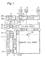
- Each of the memory cells is connected to one of the word lines WL 0 , WL 1 , ..., WL 255 and to one of the bit lines BL 0 , BL 1 , ..., BL 255 .
- Row address buffers 2 convert a transistor-transistor logic (TTL) level of row address signals A 0 , A 1 , ..., A 7 into a MOS level of row address signals A 0 , A 1 , ..., A 7 and into their inverted signals A O , A 1 , ..., A 7 , which are decoded by row address decoders and drivers 3.
- TTL transistor-transistor logic
- the row address decoders and drivers 3 select one of the word lines WL O , WL, , ..., WL 255 .
- column address buffers 4 convert a TTL level of column address signals A 0 ', A 1 ', ..., A 4 ' into a MOS level of column address signals A 0 ', ..., A 4 ' and into their inverted signals A 0 ', A 1 ', ..., A 4 ', which are decoded by column decoders 5, which drive column gates 6.
- Reference numeral 7 designates eight data input/output buffers.
- each of the input buffers comprises a level shifting circuit 7-0 for changing the potential level of an input data signal D in of one of the input/output terminals 8 from a TTL level to a MOS level while each of the output buffers comprises a sense amplifier circuit 7-1 for sensing the stored information in a memory cell so as to output output data D out to one of the input/output terminals 8.
- Reference numeral 9 designates a control signal generating circuit which receives external control signals OE and CE to generate various internal control signals to the elements 2, 3, 4, 5, 7, and the like.
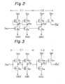
- level shifting circuit 7-0 will be explained with reference to an example in which two circuits which are driven by two different power supplies are used.
- Fig. 2 which illustrates a first prior art level shifting circuit
- enhancement/depletion (E/D)-type MOS transistors are used. That is, a first circuit Cl formed by transistors Q 1 through Q 4 is driven by a low power supply V CC of, for example, about 5 volts while a second circuit C2 formed by transistors Q 5 through Q 8 is driven by a high power supply V pp of, for example; about 20 volts.
- the potential at the node N 3 is low (GND), and, accordingly, the potential of the output D i n ' is in a floating state or low (GND).
- the voltage amplitude of the data signal D in which is, for example, of a TTL level, is converted into a large voltage amplitude (about 20 volts).
- CMOS circuits are advantageous over E/D-type MOS circuits in regard to power dissipation.
- the depletion-type transistors Q 1 , Q 3 , and Q 5 of Fig. 2 are replaced with P-channel transistors Q 11 , Q 12 , and Q 13 , respectively, and the enhancement-type transistors Q 2 , Q 4 , Q 6 , and Q 7 of Fig. 2 are replaced with N-channel transistors Q 12 , Q 14 , Q 16 , and Q 17 , respectively.
- the circuit of Fig. 3 is constructed with CMOS circuits.
- a P-channel transistor Q 18 and an N-channel transistor Q 19 are added between the first circuit Cl and the second circuit C2.
- the transistor Q 18 has a source connected to the power supply V pp , a gate connected to the node N 3 , that is, to the output of the CMOS circuit formed by the transistors Q 15 and Q16 , and a source connected to the node N 4 , that is, to the input of the CMOS circuit formed by the transistors Q 15 and Q 16 .
- the transistor Q 19 has a drain connected to the node N 2 , a gate connected to the power supply V cc , and a source connected to the node N 4 .
- the transistor Q 19 prevents a high voltage V pp from being applied to the first circuit Cl.
- V cc the potential at the node N4 increases, so that the transistor Q 19 is cut off to shut off the current flowing therethrough.
- the circuit of Fig. 4 operates stably if normal voltages are applied to the two power supply terminals, that is, if the voltage V pp is higher than the voltage V cc .
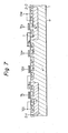
- Fig. 5 which is a cross-sectional view of the transistors Q 13 , Q 18 , and Q19 of Fig. 4, a P-type semiconductor substrate 1 in which a plurality of N-type well regions 2-1 and 2-2 are formed is used.
- N-channel transistors are formed in the P-type semiconductor substrate 1 while P-channel transistors are formed in the N-type well regions.
- a GND potential is applied to the substrate and that the power supply voltages V cc and V pp are applied to the well regions 2-1 and 2-2, respectively.
- Figure 6 is a circuit diagram illustrating a first embodiment of the semiconductor device according to the present invention.
- an N-channel transistor Q 20 is added to Fig. 5.
- This transistor Q 20 which is connected in series to the transistor Q 19 , has a drain connected to the source of the transistor Q 19 , a source connected to the node N 4 , and a gate connected to the power supply V pp .
- the gate of the transistor Q 20 remains at the GND potential, even when the data signal D in is high, so as to increase the potential at the node N 5 . Therefore, the transistor Q 20 is cut off, and, as a result, the potential at the node N 4 does not increase.
- FIG. 8 is a circuit diagram illustrating a second embodiment of the semiconductor device according to the present invention
- Fig. 9 is a partial cross-sectional view of the device of Fig. 8.
- a circuit Cl' is provided instead of the first circuit Cl of Fig. 7.
- the circuit Cl' is driven by the power supply V cc and generates an output having about the same potential as the voltage V .
- the circuit Cl' is not provided in the semiconductor substrate, which is, in this case, a P-type semiconductor substrate, while the other elements Q 15 through Q 20 are provided in the semiconductor substrate.
- the circuit Cl' comprises a connection L connected between the power supply V cc and the source of the transistor Q 19 .
- a device formed on a P-type semiconductor.substrate is illustrated.
- the present invention can also be applied to a device formed on an N-type semiconductor substrate.
- the circuit of Fig. 6 cannot be constructed by using an N-type semiconductor substrate since, in this case, the substrate must be connected to the power supply V Pp , and in addition, P -type regions and P-type wells within the substrate both cannot be connected to the power supply V cc (which may forward-bias PN junctions).
- the circuit of Fig. 8 is constructed by using an N-type semiconductor substrate as illustrated in Fig. 10.
- reference numeral 1' designates an N-type semiconductor substrate connected to the power supply V pp
- 2' designates a P-type well region connected to the GND potential.
- P-channel transistors are formed in the substrate 1' while N-channel transistors are formed in the well regions, such as 2'.
- the sequence of supplying power is not restricted.
Applications Claiming Priority (2)
| Application Number | Priority Date | Filing Date | Title |
|---|---|---|---|
| JP56189442A JPS5891680A (ja) | 1981-11-26 | 1981-11-26 | 半導体装置 |
| JP189442/81 | 1981-11-26 |
Publications (3)
| Publication Number | Publication Date |
|---|---|
| EP0090116A2 true EP0090116A2 (fr) | 1983-10-05 |
| EP0090116A3 EP0090116A3 (en) | 1985-01-23 |
| EP0090116B1 EP0090116B1 (fr) | 1987-01-28 |
Family
ID=16241313
Family Applications (1)
| Application Number | Title | Priority Date | Filing Date |
|---|---|---|---|
| EP82306286A Expired EP0090116B1 (fr) | 1981-11-26 | 1982-11-25 | Dispositif semi-conducteur CMOS comportant deux sources d'alimentation |
Country Status (5)
| Country | Link |
|---|---|
| US (1) | US4506164A (fr) |
| EP (1) | EP0090116B1 (fr) |
| JP (1) | JPS5891680A (fr) |
| DE (1) | DE3275334D1 (fr) |
| IE (1) | IE54239B1 (fr) |
Cited By (8)
| Publication number | Priority date | Publication date | Assignee | Title |
|---|---|---|---|---|
| EP0143596A2 (fr) * | 1983-11-24 | 1985-06-05 | Fujitsu Limited | Dispositif de mémoire morte programmable |
| EP0204499A2 (fr) * | 1985-05-29 | 1986-12-10 | Advanced Micro Devices, Inc. | Circuit d'isolation haute tension pour réseaux CMOS |
| EP0206710A2 (fr) * | 1985-06-17 | 1986-12-30 | Advanced Micro Devices, Inc. | Interrupteur CMOS à haute tension |
| EP0209805A2 (fr) * | 1985-07-22 | 1987-01-28 | Hitachi, Ltd. | Dispositif à semi-conducteurs à transistor bipolaire et transistor à effet de champ à grille isolée |
| EP0254139A2 (fr) * | 1986-07-09 | 1988-01-27 | Kabushiki Kaisha Toshiba | Dispositif de mémoire non-volatile à semi-conducteurs |
| EP0357502A2 (fr) * | 1988-08-30 | 1990-03-07 | Fujitsu Limited | Circuit de mémoire programmable à semi-conducteurs |
| EP0385469A2 (fr) * | 1989-03-03 | 1990-09-05 | Kabushiki Kaisha Toshiba | Circuit de détection de potentiel |
| US6125075A (en) * | 1985-07-22 | 2000-09-26 | Hitachi, Ltd. | Semiconductor device incorporating internal power supply for compensating for deviation in operating condition and fabrication process conditions |
Families Citing this family (52)
| Publication number | Priority date | Publication date | Assignee | Title |
|---|---|---|---|---|
| JPS5990292A (ja) * | 1982-11-12 | 1984-05-24 | Toshiba Corp | 電圧変換回路 |
| JPH0680803B2 (ja) * | 1983-07-19 | 1994-10-12 | 株式会社東芝 | Misダイナミックメモリセル及びmisダイナミックメモリセルの製造方法 |
| DE3339253A1 (de) * | 1983-10-28 | 1985-05-09 | Siemens AG, 1000 Berlin und 8000 München | Cmos-inverter |
| US4565932A (en) * | 1983-12-29 | 1986-01-21 | Motorola, Inc. | High voltage circuit for use in programming memory circuits (EEPROMs) |
| NL8400326A (nl) * | 1984-02-03 | 1985-09-02 | Philips Nv | Geintegreerde schakeling met veldeffecttransistoren en een programmeerbaar leesgeheugen. |
| US4638182A (en) * | 1984-07-11 | 1987-01-20 | Texas Instruments Incorporated | High-level CMOS driver circuit |
| US4814646A (en) * | 1985-03-22 | 1989-03-21 | Monolithic Memories, Inc. | Programmable logic array using emitter-coupled logic |
| JPS6269719A (ja) * | 1985-09-24 | 1987-03-31 | Toshiba Corp | レベル変換論理回路 |
| NL8503331A (nl) * | 1985-12-03 | 1987-07-01 | Philips Nv | Geintegreerde schakeling bevattende een lastkapaciteit en geintegreerde referentiebron. |
| JPS62170098A (ja) * | 1986-01-21 | 1987-07-27 | Fujitsu Ltd | 半導体集積回路 |
| US4760283A (en) * | 1986-08-29 | 1988-07-26 | Texas Instruments Incorporated | Dynamic input latch |
| JPS63131396A (ja) * | 1986-11-20 | 1988-06-03 | Ricoh Co Ltd | 半導体メモリ装置のセンス回路 |
| JP2585348B2 (ja) * | 1988-02-22 | 1997-02-26 | 株式会社東芝 | 不揮発性半導体記憶装置 |
| US5084637A (en) * | 1989-05-30 | 1992-01-28 | International Business Machines Corp. | Bidirectional level shifting interface circuit |
| US4963765A (en) * | 1989-07-03 | 1990-10-16 | Texas Instruments Incorporated | High speed CMOS transition detector circuit |
| US5151616A (en) * | 1990-01-23 | 1992-09-29 | Nec Corporation | Cmos high voltage switch |
| GB9007791D0 (en) * | 1990-04-06 | 1990-06-06 | Foss Richard C | High voltage boosted wordline supply charge pump and regulator for dram |
| GB9007790D0 (en) * | 1990-04-06 | 1990-06-06 | Lines Valerie L | Dynamic memory wordline driver scheme |
| IT1243691B (it) * | 1990-07-27 | 1994-06-21 | Sgs Thomson Microelectronics | Traslatore di livello a transistore singolo, con bassa impedenza dinamica, in tecnologia cmos |
| US5128560A (en) * | 1991-03-22 | 1992-07-07 | Micron Technology, Inc. | Boosted supply output driver circuit for driving an all N-channel output stage |
| JP3151329B2 (ja) * | 1993-04-07 | 2001-04-03 | 株式会社東芝 | データ出力回路 |
| JP3267436B2 (ja) * | 1993-04-19 | 2002-03-18 | 三菱電機株式会社 | 半導体装置 |
| JPH0758623A (ja) * | 1993-08-20 | 1995-03-03 | Mitsubishi Electric Corp | Cmos入力回路 |
| JP3173247B2 (ja) * | 1993-09-29 | 2001-06-04 | ソニー株式会社 | レベルシフタ |
| JP3160449B2 (ja) * | 1993-12-02 | 2001-04-25 | 株式会社東芝 | トランジスタ回路 |
| US5796673A (en) * | 1994-10-06 | 1998-08-18 | Mosaid Technologies Incorporated | Delay locked loop implementation in a synchronous dynamic random access memory |
| JP3369384B2 (ja) * | 1995-07-12 | 2003-01-20 | 三菱電機株式会社 | 出力バッファ回路 |
| US5644265A (en) * | 1995-05-01 | 1997-07-01 | International Business Machines Corporation | Off-chip driver for mixed voltage applications |
| JPH09148914A (ja) * | 1995-11-21 | 1997-06-06 | Sony Corp | レベル変換回路 |
| US6175952B1 (en) * | 1997-05-27 | 2001-01-16 | Altera Corporation | Technique of fabricating integrated circuits having interfaces compatible with different operating voltage conditions |
| US6118302A (en) | 1996-05-28 | 2000-09-12 | Altera Corporation | Interface for low-voltage semiconductor devices |
| JPH10285013A (ja) * | 1997-04-08 | 1998-10-23 | Mitsubishi Electric Corp | 出力バッファ回路 |
| JP3137030B2 (ja) * | 1997-04-18 | 2001-02-19 | 日本電気株式会社 | 半導体装置 |
| US6278294B1 (en) | 1997-05-01 | 2001-08-21 | Mitsubishi Denki Kabushiki Kaisha | Output buffer circuit |
| JP3123463B2 (ja) * | 1997-05-16 | 2001-01-09 | 日本電気株式会社 | レベル変換回路 |
| JPH11102305A (ja) * | 1997-09-29 | 1999-04-13 | Oki Electric Ind Co Ltd | インサーキットエミュレータ |
| US6154059A (en) * | 1997-11-25 | 2000-11-28 | Altera Corporation | High performance output buffer |
| JP2000228627A (ja) * | 1999-02-05 | 2000-08-15 | Mitsubishi Electric Corp | 入出力回路 |
| JP2002353805A (ja) * | 2001-05-30 | 2002-12-06 | Fujitsu Ltd | 半導体回路 |
| US6545521B2 (en) | 2001-06-29 | 2003-04-08 | International Business Machines Corporation | Low skew, power sequence independent CMOS receiver device |
| JP3889954B2 (ja) * | 2001-10-29 | 2007-03-07 | 株式会社ルネサステクノロジ | 半導体装置 |
| US6844770B2 (en) * | 2002-04-17 | 2005-01-18 | Virtual Silicon Technology, Inc. | Circuitry to provide a low power input buffer |
| EP2005591A1 (fr) * | 2006-03-30 | 2008-12-24 | Tte Technology, Inc. | Circuit de communication doté d'une tension de signal sélectionnable |
| US7855574B2 (en) * | 2006-10-10 | 2010-12-21 | Altera Corporation | Programmable multiple supply regions with switched pass gate level converters |
| US7429875B2 (en) * | 2006-12-13 | 2008-09-30 | Lattice Semiconductor Corporation | Low static current drain logic circuit |
| US20080201502A1 (en) * | 2007-02-15 | 2008-08-21 | Inventec Corporation | Sync circuit of data transmission interface |
| US7564290B2 (en) * | 2007-10-09 | 2009-07-21 | International Business Machines Corporation | Design structure for a high-speed level shifter |
| US8138814B2 (en) | 2008-07-29 | 2012-03-20 | Qualcomm Incorporated | High signal level compliant input/output circuits |
| US8106699B2 (en) * | 2008-07-29 | 2012-01-31 | Qualcomm Incorporated | High signal level compliant input/output circuits |
| US7804334B2 (en) * | 2008-07-29 | 2010-09-28 | Qualcomm Incorporated | High signal level compliant input/output circuits |
| US8593203B2 (en) * | 2008-07-29 | 2013-11-26 | Qualcomm Incorporated | High signal level compliant input/output circuits |
| US7772887B2 (en) | 2008-07-29 | 2010-08-10 | Qualcomm Incorporated | High signal level compliant input/output circuits |
Citations (1)
| Publication number | Priority date | Publication date | Assignee | Title |
|---|---|---|---|---|
| US4039869A (en) * | 1975-11-28 | 1977-08-02 | Rca Corporation | Protection circuit |
Family Cites Families (6)
| Publication number | Priority date | Publication date | Assignee | Title |
|---|---|---|---|---|
| US3916430A (en) * | 1973-03-14 | 1975-10-28 | Rca Corp | System for eliminating substrate bias effect in field effect transistor circuits |
| US4080539A (en) * | 1976-11-10 | 1978-03-21 | Rca Corporation | Level shift circuit |
| US4239994A (en) * | 1978-08-07 | 1980-12-16 | Rca Corporation | Asymmetrically precharged sense amplifier |
| US4216390A (en) * | 1978-10-04 | 1980-08-05 | Rca Corporation | Level shift circuit |
| US4317110A (en) * | 1980-06-30 | 1982-02-23 | Rca Corporation | Multi-mode circuit |
| US4463273A (en) * | 1981-10-26 | 1984-07-31 | Rca Corporation | Electronic circuits and structures employing enhancement and depletion type IGFETs |
-
1981
- 1981-11-26 JP JP56189442A patent/JPS5891680A/ja active Granted
-
1982
- 1982-11-24 IE IE2797/82A patent/IE54239B1/en not_active IP Right Cessation
- 1982-11-24 US US06/444,482 patent/US4506164A/en not_active Expired - Lifetime
- 1982-11-25 DE DE8282306286T patent/DE3275334D1/de not_active Expired
- 1982-11-25 EP EP82306286A patent/EP0090116B1/fr not_active Expired
Patent Citations (1)
| Publication number | Priority date | Publication date | Assignee | Title |
|---|---|---|---|---|
| US4039869A (en) * | 1975-11-28 | 1977-08-02 | Rca Corporation | Protection circuit |
Non-Patent Citations (2)
| Title |
|---|
| IEEE JOURNAL OF SOLID-STATE CIRCUITS, vol. 14, no. 5, October 1979, pages 860-864, IEEE, New York, USA; R.G. STEWART: "CMOS/SOS EAROM memory arrays" * |
| IEEE JOURNAL OF SOLID-STATE CIRCUITS, vol. SC-13, no. 5, October 1978, pages 677-680, IEEE, New York, USA; Y.-F. CHAN: "A 4K CMOS erasable PROM" * |
Cited By (20)
| Publication number | Priority date | Publication date | Assignee | Title |
|---|---|---|---|---|
| EP0143596A3 (en) * | 1983-11-24 | 1987-09-02 | Fujitsu Limited | Programmable read-only memory device |
| EP0143596A2 (fr) * | 1983-11-24 | 1985-06-05 | Fujitsu Limited | Dispositif de mémoire morte programmable |
| EP0204499A2 (fr) * | 1985-05-29 | 1986-12-10 | Advanced Micro Devices, Inc. | Circuit d'isolation haute tension pour réseaux CMOS |
| EP0204499A3 (fr) * | 1985-05-29 | 1988-12-14 | Advanced Micro Devices, Inc. | Circuit d'isolation haute tension pour réseaux CMOS |
| EP0206710A3 (fr) * | 1985-06-17 | 1988-10-26 | Advanced Micro Devices, Inc. | Interrupteur CMOS à haute tension |
| EP0206710A2 (fr) * | 1985-06-17 | 1986-12-30 | Advanced Micro Devices, Inc. | Interrupteur CMOS à haute tension |
| EP0209805A2 (fr) * | 1985-07-22 | 1987-01-28 | Hitachi, Ltd. | Dispositif à semi-conducteurs à transistor bipolaire et transistor à effet de champ à grille isolée |
| EP0209805B1 (fr) * | 1985-07-22 | 1993-04-07 | Hitachi, Ltd. | Dispositif à semi-conducteurs à transistor bipolaire et transistor à effet de champ à grille isolée |
| US6970391B2 (en) | 1985-07-22 | 2005-11-29 | Renesas Technology Corporation | Semiconductor device incorporating internal power supply for compensating for deviation in operating condition and fabrication process conditions |
| US6363029B1 (en) | 1985-07-22 | 2002-03-26 | Hitachi, Ltd. | Semiconductor device incorporating internal power supply for compensating for deviation in operating condition and fabrication process conditions |
| US6125075A (en) * | 1985-07-22 | 2000-09-26 | Hitachi, Ltd. | Semiconductor device incorporating internal power supply for compensating for deviation in operating condition and fabrication process conditions |
| EP0433271A2 (fr) * | 1985-07-22 | 1991-06-19 | Hitachi, Ltd. | Dispositif à semi-conducteurs |
| EP0433271A3 (en) * | 1985-07-22 | 1991-11-06 | Hitachi, Ltd. | Semiconductor device |
| EP0254139A2 (fr) * | 1986-07-09 | 1988-01-27 | Kabushiki Kaisha Toshiba | Dispositif de mémoire non-volatile à semi-conducteurs |
| EP0254139A3 (fr) * | 1986-07-09 | 1991-01-09 | Kabushiki Kaisha Toshiba | Dispositif de mémoire non-volatile à semi-conducteurs |
| US7002856B2 (en) | 1986-07-18 | 2006-02-21 | Renesas Technology Corporation | Semiconductor device incorporating internal power supply for compensating for deviation in operating condition and fabrication process conditions |
| EP0357502A3 (fr) * | 1988-08-30 | 1992-01-02 | Fujitsu Limited | Circuit de mémoire programmable à semi-conducteurs |
| EP0357502A2 (fr) * | 1988-08-30 | 1990-03-07 | Fujitsu Limited | Circuit de mémoire programmable à semi-conducteurs |
| EP0385469A3 (fr) * | 1989-03-03 | 1992-04-08 | Kabushiki Kaisha Toshiba | Circuit de détection de potentiel |
| EP0385469A2 (fr) * | 1989-03-03 | 1990-09-05 | Kabushiki Kaisha Toshiba | Circuit de détection de potentiel |
Also Published As
| Publication number | Publication date |
|---|---|
| JPS5891680A (ja) | 1983-05-31 |
| IE54239B1 (en) | 1989-08-02 |
| EP0090116A3 (en) | 1985-01-23 |
| JPH0143464B2 (fr) | 1989-09-20 |
| IE822797L (en) | 1983-05-26 |
| EP0090116B1 (fr) | 1987-01-28 |
| DE3275334D1 (en) | 1987-03-05 |
| US4506164A (en) | 1985-03-19 |
Similar Documents
| Publication | Publication Date | Title |
|---|---|---|
| EP0090116B1 (fr) | Dispositif semi-conducteur CMOS comportant deux sources d'alimentation | |
| US4404659A (en) | Programmable read only memory | |
| KR970003809B1 (ko) | 소거특성을 개량한 플래쉬메모리 및 그것에 대한 회로 | |
| US5039882A (en) | Address decoder circuit for non-volatile memory | |
| US5253201A (en) | Writing control circuit employed in non-volatile semiconductor memory device | |
| US5392253A (en) | Nonvolatile semiconductor memory device having row decoder supplying a negative potential to word lines during erase mode | |
| US7339828B2 (en) | Nonvolatile semiconductor memory device with memory cells, each having an FG cell transistor and select gate transistor, and a method of writing data into the same | |
| KR0155078B1 (ko) | 강전계용의 mos 회로를 갖춘 반도체 회로 | |
| US6243292B1 (en) | Nonvolatile semiconductor memory device capable of reducing memory array area | |
| EP0522579A2 (fr) | Circuit de décalage de niveau pour circuits intégrés | |
| JPH0562486A (ja) | 集積回路用スイツチ | |
| KR910007436B1 (ko) | 반도체 비휘발성 메모리 장치 | |
| US5818758A (en) | Zero voltage drop negative switch for dual well processes | |
| JPH02187994A (ja) | 半導体記憶装置 | |
| EP0029716A2 (fr) | Dispositif de mémoire programmable à semi-conducteurs | |
| US6128230A (en) | Semiconductor memory with PN junction potential reduction in a writing mode | |
| KR100346991B1 (ko) | 반도체 기억 장치 | |
| KR0180329B1 (ko) | 상이한 전력 전압을 선택적으로 공급하는 간단하고 안정된 전환 회로를 갖는 반도체 장치 | |
| US6013932A (en) | Supply voltage reduction circuit for integrated circuit | |
| US5719490A (en) | Dual sourced voltage supply circuit | |
| US5808935A (en) | Common source line driving circuit for use in nonvolatile semiconductor memories | |
| US6049498A (en) | Double transistor switch for supplying multiple voltages to flash memory wordlines | |
| EP0164868A2 (fr) | Mémoire morte programmable et effaçable | |
| US5691944A (en) | Non-volatile semiconductor memory device | |
| US5295113A (en) | Flash memory source inhibit generator |
Legal Events
| Date | Code | Title | Description |
|---|---|---|---|
| PUAI | Public reference made under article 153(3) epc to a published international application that has entered the european phase |
Free format text: ORIGINAL CODE: 0009012 |
|
| AK | Designated contracting states |
Designated state(s): DE FR GB |
|
| PUAL | Search report despatched |
Free format text: ORIGINAL CODE: 0009013 |
|
| AK | Designated contracting states |
Designated state(s): DE FR GB |
|
| 17P | Request for examination filed |
Effective date: 19841228 |
|
| 17Q | First examination report despatched |
Effective date: 19860415 |
|
| GRAA | (expected) grant |
Free format text: ORIGINAL CODE: 0009210 |
|
| AK | Designated contracting states |
Kind code of ref document: B1 Designated state(s): DE FR GB |
|
| ET | Fr: translation filed | ||
| REF | Corresponds to: |
Ref document number: 3275334 Country of ref document: DE Date of ref document: 19870305 |
|
| PLBE | No opposition filed within time limit |
Free format text: ORIGINAL CODE: 0009261 |
|
| STAA | Information on the status of an ep patent application or granted ep patent |
Free format text: STATUS: NO OPPOSITION FILED WITHIN TIME LIMIT |
|
| 26N | No opposition filed | ||
| PGFP | Annual fee paid to national office [announced via postgrant information from national office to epo] |
Ref country code: FR Payment date: 20011113 Year of fee payment: 20 |
|
| PGFP | Annual fee paid to national office [announced via postgrant information from national office to epo] |
Ref country code: GB Payment date: 20011128 Year of fee payment: 20 |
|
| PGFP | Annual fee paid to national office [announced via postgrant information from national office to epo] |
Ref country code: DE Payment date: 20011210 Year of fee payment: 20 |
|
| REG | Reference to a national code |
Ref country code: GB Ref legal event code: IF02 |
|
| PG25 | Lapsed in a contracting state [announced via postgrant information from national office to epo] |
Ref country code: GB Free format text: LAPSE BECAUSE OF EXPIRATION OF PROTECTION Effective date: 20021124 |
|
| REG | Reference to a national code |
Ref country code: GB Ref legal event code: PE20 Effective date: 20021124 |