EP0086349B1 - Display device - Google Patents
Display device Download PDFInfo
- Publication number
- EP0086349B1 EP0086349B1 EP83100476A EP83100476A EP0086349B1 EP 0086349 B1 EP0086349 B1 EP 0086349B1 EP 83100476 A EP83100476 A EP 83100476A EP 83100476 A EP83100476 A EP 83100476A EP 0086349 B1 EP0086349 B1 EP 0086349B1
- Authority
- EP
- European Patent Office
- Prior art keywords
- electrode
- picture
- display device
- film
- transparent
- Prior art date
- Legal status (The legal status is an assumption and is not a legal conclusion. Google has not performed a legal analysis and makes no representation as to the accuracy of the status listed.)
- Expired
Links
Images


Classifications
-
- G—PHYSICS
- G02—OPTICS
- G02F—OPTICAL DEVICES OR ARRANGEMENTS FOR THE CONTROL OF LIGHT BY MODIFICATION OF THE OPTICAL PROPERTIES OF THE MEDIA OF THE ELEMENTS INVOLVED THEREIN; NON-LINEAR OPTICS; FREQUENCY-CHANGING OF LIGHT; OPTICAL LOGIC ELEMENTS; OPTICAL ANALOGUE/DIGITAL CONVERTERS
- G02F1/00—Devices or arrangements for the control of the intensity, colour, phase, polarisation or direction of light arriving from an independent light source, e.g. switching, gating or modulating; Non-linear optics
- G02F1/01—Devices or arrangements for the control of the intensity, colour, phase, polarisation or direction of light arriving from an independent light source, e.g. switching, gating or modulating; Non-linear optics for the control of the intensity, phase, polarisation or colour
- G02F1/13—Devices or arrangements for the control of the intensity, colour, phase, polarisation or direction of light arriving from an independent light source, e.g. switching, gating or modulating; Non-linear optics for the control of the intensity, phase, polarisation or colour based on liquid crystals, e.g. single liquid crystal display cells
- G02F1/133—Constructional arrangements; Operation of liquid crystal cells; Circuit arrangements
- G02F1/136—Liquid crystal cells structurally associated with a semi-conducting layer or substrate, e.g. cells forming part of an integrated circuit
- G02F1/1362—Active matrix addressed cells
- G02F1/1368—Active matrix addressed cells in which the switching element is a three-electrode device
-
- H—ELECTRICITY
- H10—SEMICONDUCTOR DEVICES; ELECTRIC SOLID-STATE DEVICES NOT OTHERWISE PROVIDED FOR
- H10W—GENERIC PACKAGES, INTERCONNECTIONS, CONNECTORS OR OTHER CONSTRUCTIONAL DETAILS OF DEVICES COVERED BY CLASS H10
- H10W72/00—Interconnections or connectors in packages
-
- G—PHYSICS
- G02—OPTICS
- G02F—OPTICAL DEVICES OR ARRANGEMENTS FOR THE CONTROL OF LIGHT BY MODIFICATION OF THE OPTICAL PROPERTIES OF THE MEDIA OF THE ELEMENTS INVOLVED THEREIN; NON-LINEAR OPTICS; FREQUENCY-CHANGING OF LIGHT; OPTICAL LOGIC ELEMENTS; OPTICAL ANALOGUE/DIGITAL CONVERTERS
- G02F1/00—Devices or arrangements for the control of the intensity, colour, phase, polarisation or direction of light arriving from an independent light source, e.g. switching, gating or modulating; Non-linear optics
- G02F1/01—Devices or arrangements for the control of the intensity, colour, phase, polarisation or direction of light arriving from an independent light source, e.g. switching, gating or modulating; Non-linear optics for the control of the intensity, phase, polarisation or colour
- G02F1/13—Devices or arrangements for the control of the intensity, colour, phase, polarisation or direction of light arriving from an independent light source, e.g. switching, gating or modulating; Non-linear optics for the control of the intensity, phase, polarisation or colour based on liquid crystals, e.g. single liquid crystal display cells
- G02F1/133—Constructional arrangements; Operation of liquid crystal cells; Circuit arrangements
- G02F1/1333—Constructional arrangements; Manufacturing methods
- G02F1/1335—Structural association of cells with optical devices, e.g. polarisers or reflectors
- G02F1/133509—Filters, e.g. light shielding masks
- G02F1/133512—Light shielding layers, e.g. black matrix
-
- G—PHYSICS
- G02—OPTICS
- G02F—OPTICAL DEVICES OR ARRANGEMENTS FOR THE CONTROL OF LIGHT BY MODIFICATION OF THE OPTICAL PROPERTIES OF THE MEDIA OF THE ELEMENTS INVOLVED THEREIN; NON-LINEAR OPTICS; FREQUENCY-CHANGING OF LIGHT; OPTICAL LOGIC ELEMENTS; OPTICAL ANALOGUE/DIGITAL CONVERTERS
- G02F2202/00—Materials and properties
- G02F2202/10—Materials and properties semiconductor
- G02F2202/104—Materials and properties semiconductor poly-Si
Definitions
- the present invention relates to a thin-film transistor addressed display device. It is applicable to, for example, a liquid-crystal display device or electroluminescent display device of the active- matrix addressing type.
- the substrate of picture elements is desired to be transparent.
- the selection of a displaying mode becomes more versatile.
- a picture of high contrast ratio can be formed, for example, in such a way that transmissive-type liquid-crystal display elements with a twisted nematic liquid-crystal layer held between two polarizers are illuminated from the rear.
- Another advantage is that a color display device can be readily provided by the use of lights which are transmitted through filters of three colors.
- a transparent substrate such as glass and quartz is used for rendering the picture element parts transparent and that a semiconductor film constituting the thin-film transistors is formed in selected parts outside the picture elements.
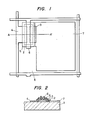
- the semiconductor film 2 is formed as the islands on a transparent insulating substrate 1.
- a source electrode 3 is electrically connected with one transparent electrode 7 of a display element (for example, liquid-crystal element).
- a drain electrode 4 serves also as a signal electrode.
- a gate electrode 6, which is formed on a gate insulating film 5, serves also as a scanning electrode.
- Numeral 8 indicates an area where neither an electrode nor a semiconductor material is disposed.
- thin-film transistors in accordance with a fabrication process similar to that of single-crystal silicon devices by employing, e.g., a polycrystalline silicon film.
- patterns are formed by the use of photolithographic techniques. This is desirable from the viewpoints of improving the characteristics of the thin-film transistors and rendering the precision of interconnection patterns high.
- the display device is desired to have the transparent substrate of the picture elements. It is accordingly desirable to selectively etch the semiconductor film constituting the thin-film transistors, by the photolithographic techniques, so as to remove the parts of the semiconductor film corresponding to the picture elements. In this case, when the semiconductor film is left as the islands, a problem stated hereunder arises.
- the section of the pattern formed by the photolithographic techniques changes abruptly from a film thickness dto a film thickness o.
- this has led to the disadvantage that, when an electrode bus 12 is formed on the film 11 having such stepped part, it is liable to disconnection as indicated at numeral 13.
- the switching matrix of the thin-film transistors which are formed on the semiconductor film selectively etched into the islands by the photolithographic techniques, has had the disadvantage that defects ascribable to the disconnection of the interconnection bus are prone to occur.
- Another disadvantage of the prior-art switching matrix of the thin-film transistors having the structure as shown in Figure 1, is that when the switching matrix is applied to a display device, the contrast of display viewed as a whole is inferior. More specifically, with the structure as shown in Figure 1, there are the parts as indicated at numeral 8, which are not electrode portions and which are not covered with the semiconductor film, either. In case of, e.g., a liquid-crystal display device, accordingly, liquid crystal on the part 8 has no voltage applied thereto and is overlaid with no material for shielding it from light, so that the light transmissivity for the part 8 is always great in some liquid crystal modes of operation.
- the display device which employs the prior-art switching matrix of the structure as shown in Figure 1 has had, in some displaying modes, the disadvantage that the contrast of display viewed as a whole is inferior.
- this disadvantage can be eliminated in such a way that a mask adapted to shield the transmitted lights of parts irrelevant to the display is disposed outside.
- the object of the present invention is to provide a display device including an active matrix having a structure in which electrode buses are less prone to disconnection even in case of forming an active matrix of thin-film transistors by the use of photolithographic techniques, and according to which the display device can display a good picture of few defects and to provide the matrix structure of the thin-film transistors so that fabrication is simple and a good contrast ratio of display can be effected.
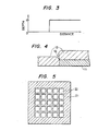
- a poly-Si film is formed on a quartz substrate to a thickness of 1 pm, and it is selectively etched in the shape of meshes as shown in Figure 5.
- the poly-Si film is evaporated, for example, in ultrahigh vacuum with a pressure below 10- 8 Torr.
- Figure 5 is a schematic plan view of the poly-Si meshes for the whole display device.
- the poly-Si film is selectively etched so as to leave a hatched part 21 behind. Parts 22 where the poly-Si film has been removed, become picture element parts.
- the transparent insulating substrate is exposed to these parts 22.
- Figure 6 is a plan view of a switching matrix with one picture element thereof enlarged, while Figure 7 is a sectional view taken along B-B' in Figure 6.
- a metal-oxide-semiconductor (MOS) field-effect transistor is formed, which is provided with a source electrode 24, a drain and signal electrode bus 25 and a gate and scanning electrode bus 26, 26'.
- the signal electrode bus 25 and the scanning electrode bus 26' form two-level interconnection layers insulated by an insulator, at the point of intersection 50 thereof.
- a transparent picture-element electrode (5,000 A thick) 27 of indium-tin-oxide or the like is formed.
- This transparent picture-element electrode is put into a structure in which it can be electrically connected with the source electrode 24 and in which it covers the picture element part 22 with the poly-Si film removed therefrom.
- the transparent electrode can be satisfactorily formed by a conventional method, for example, the sputtering process or the evaporation process.
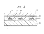
- a transparent common electrode 32 of indium-tin-oxide or the like is disposed in opposition to the transparent picture-element electrodes 27 which is connected with the thin-film transistors 31 formed as described above, and a liquid crystal 33, for example, PCH (phenyl cyclohexane)-based liquid crystal or biphenyl-based liquid crystal is contained between the transistors and the common electrode.
- PCH phenyl cyclohexane
- each thin-film transistor 31 has its section constructed as shown in Figure 7.
- the gap between the transparent picture-element electrode 27 and the transparent common electrode 32, namely, the thickness of the liquid-crystal layer is 10 Il m.
- the way of constructing the liquid-crystal display device itself is similar to that in the prior art. Only the construction on one faceplate is different.
- the transparent common electrode 32 is supported by a glass substrate 34. Shown at numeral 20 is the quartz substrate on which the switching matrix has been formed.
- the source electrode 24, the drain and signal electrode bus 25 and the gate electrode 26 are formed of aluminum, and the scanning electrode bus 26' is formed of a multi-layer film of Cr and Au.
- Cr is for bonding and is about 500 A thick, and Au is about 5,000 A thick.
- any of the source electrode 24, the drain and signal electrode bus 25, the gate electrode 26 and the scanning electrode 26' does not traverse the stepped portion of the poly-Si film. Accordingly, the possibility of the disconnection of the three spaced electrodes ascribable to the stepped portion of the poly-Si film is eliminated. According to an example of the present embodiment, a good picture of few defects could be displayed.
- the transparent picture-element electrode 27 inevitably becomes a structure in which it strides over the stepped portion of the poly-Si film. Since, however, the transparent picture-element electrode 27 may join to a part of the long stepped portion, the disconnection of the transparent picture-element electrode was not caused by the stepped portion.
- the poly-Si film formed in the shape of meshes is small in the light transmissivity irrespective of voltages applied to the respective picture elements, it shields the transmitted lights of portions irrelevant to the display.
- the contrast ratio of the display viewed as a whole was enhanced.
- the occupying area of picture elements is 60% with respect to the whole screen.
- the contrast ratio of a picture degrades to about 2.5 independent of that of the picture elements themselves.
- the contrast ratio of the picture elements themselves which is usually more than 20 can be secured.
- a mask which shields the transmitted lights of parts irrelevant to the display is not especially provided, but the shape of the semiconductor film which is a constituent material of the thin-film transistors is contrived thereby to assign the function of the above mask to the semiconductor film.
- the additional mask need not be disposed, the production process is simplified and the production cost can be reduced, so that the present invention has a high industrial value.
- Figure 9 is a plan view showing one picture element of the embodiment of a switching matrix of thin-film transistors for the EL display device.
- a semiconductor film 41 etched in the shape of meshes, there are formed two thin-film transistors 42 and 43 and the three electrode buses of a power electrode bus 44, a scanning electrode bus 45 and a signal electrode bus 46, which are coupled with the picture element electrode 51 of an EL-element 47 and capacitor 48.
- the semiconductor film is left unetched in parts other than the portions of EL elements.
- An equivalent circuit of the device is as shown in Figure 10. This circuit is customary as the transistor matrix for driving EL elements.
- the thin-film transistor matrix is overlaid with the EL elements 47 which are further overlaid with a common counter electrode 49.
- the EL-element 47 is so constructed that, for example, an active layer of ZnS: Mn having a thickness of 5000 A is sandwiched between insulating layers, for example, S M2 0 3 films having a thickness of 2000 A.
- Either the picture element electrode 51 or the common counter electrode 49 is formed of a transparent electrode so as to derive light emitted therefrom. Since, in this case, the light emitting elements are used, it does not occur that parts irrelevant to display lower the contrast of the display. Therefore, the present embodiment does not bring forth the second effect of the present invention, namely, the effect of enhancing the display quality. In the present embodiment, however, the electrode buses are less prone to disconnection owing to the present invention. Accordingly, an EL display device which displays a good picture of few defects has been obtained.
- the present invention is applicable to various display devices.
- the disconnection of electrode buses can be reduced, and transmitted lights through parts irrelevant to display can be shielded without employing any special mask. According to the present invention, therefore, a display device which displays a picture of good quality having few defects and exhibiting a favorable contrast ratio can be fabricated simply and at low cost. This is greatly effective in industry.
Landscapes
- Physics & Mathematics (AREA)
- Nonlinear Science (AREA)
- Engineering & Computer Science (AREA)
- Microelectronics & Electronic Packaging (AREA)
- Mathematical Physics (AREA)
- Chemical & Material Sciences (AREA)
- Crystallography & Structural Chemistry (AREA)
- General Physics & Mathematics (AREA)
- Optics & Photonics (AREA)
- Liquid Crystal (AREA)
- Devices For Indicating Variable Information By Combining Individual Elements (AREA)
- Electroluminescent Light Sources (AREA)
Applications Claiming Priority (2)
| Application Number | Priority Date | Filing Date | Title |
|---|---|---|---|
| JP22744/82 | 1982-02-17 | ||
| JP57022744A JPS58140781A (ja) | 1982-02-17 | 1982-02-17 | 画像表示装置 |
Publications (2)
| Publication Number | Publication Date |
|---|---|
| EP0086349A1 EP0086349A1 (en) | 1983-08-24 |
| EP0086349B1 true EP0086349B1 (en) | 1986-05-07 |
Family
ID=12091206
Family Applications (1)
| Application Number | Title | Priority Date | Filing Date |
|---|---|---|---|
| EP83100476A Expired EP0086349B1 (en) | 1982-02-17 | 1983-01-20 | Display device |
Country Status (6)
| Country | Link |
|---|---|
| US (1) | US4904989A (enExample) |
| EP (1) | EP0086349B1 (enExample) |
| JP (1) | JPS58140781A (enExample) |
| KR (1) | KR860000229B1 (enExample) |
| CA (1) | CA1207420A (enExample) |
| DE (1) | DE3363314D1 (enExample) |
Families Citing this family (27)
| Publication number | Priority date | Publication date | Assignee | Title |
|---|---|---|---|---|
| JPS60227235A (ja) * | 1984-04-26 | 1985-11-12 | Canon Inc | 画像形成装置 |
| FR2571913B1 (fr) * | 1984-10-17 | 1986-12-26 | Richard Joseph | Ecran d'affichage a matrice active a double transistor d'adressage |
| JPH0627980B2 (ja) * | 1984-10-17 | 1994-04-13 | レタ・フランセ・ルプレザント・パ・ル・ミニストル・デ・ペ・テ・テ・(セントル・ナシヨナル・デチユ−ド・デ・テレコミユニカシオン) | 能動マトリクスデイスプレイスクリ−ンの製造方法 |
| US4688896A (en) * | 1985-03-04 | 1987-08-25 | General Electric Company | Information conversion device with auxiliary address lines for enhancing manufacturing yield |
| FR2585167B1 (fr) * | 1985-07-19 | 1993-05-07 | Gen Electric | Structures conductrices redondantes pour affichages a cristaux liquides commandes par des transistors a effet de champ en couche mince |
| US4819038A (en) * | 1986-12-22 | 1989-04-04 | Ibm Corporation | TFT array for liquid crystal displays allowing in-process testing |
| JP2769830B2 (ja) * | 1989-01-23 | 1998-06-25 | 藤森工業株式会社 | 液晶セルの製造法 |
| DE69013275T2 (de) * | 1989-08-21 | 1995-05-04 | Sharp Kk | Flüssigkristall-Anzeigevorrichtung. |
| US5194974A (en) * | 1989-08-21 | 1993-03-16 | Sharp Kabushiki Kaisha | Non-flicker liquid crystal display with capacitive charge storage |
| US5075595A (en) * | 1991-01-24 | 1991-12-24 | Motorola, Inc. | Field emission device with vertically integrated active control |
| US5212426A (en) * | 1991-01-24 | 1993-05-18 | Motorola, Inc. | Integrally controlled field emission flat display device |
| US5471225A (en) * | 1993-04-28 | 1995-11-28 | Dell Usa, L.P. | Liquid crystal display with integrated frame buffer |
| JPH0887034A (ja) * | 1994-09-16 | 1996-04-02 | Toshiba Corp | 液晶表示装置およびその製造方法 |
| KR100205259B1 (ko) * | 1996-03-04 | 1999-07-01 | 구자홍 | 액티브매트릭스 액정디스플레이의 구동회로 |
| US6462722B1 (en) | 1997-02-17 | 2002-10-08 | Seiko Epson Corporation | Current-driven light-emitting display apparatus and method of producing the same |
| EP1830344B1 (en) * | 1997-02-17 | 2012-07-04 | Seiko Epson Corporation | Structure of a pixel driving circuit for an electroluminescent display |
| US6175345B1 (en) * | 1997-06-02 | 2001-01-16 | Canon Kabushiki Kaisha | Electroluminescence device, electroluminescence apparatus, and production methods thereof |
| JP3042493B2 (ja) | 1998-05-13 | 2000-05-15 | 日本電気株式会社 | 液晶表示装置およびその駆動方法 |
| JP2000227771A (ja) | 1998-12-01 | 2000-08-15 | Sanyo Electric Co Ltd | カラーel表示装置 |
| JP2005209656A (ja) * | 1998-12-01 | 2005-08-04 | Sanyo Electric Co Ltd | カラーel表示装置 |
| JP2000227770A (ja) | 1998-12-01 | 2000-08-15 | Sanyo Electric Co Ltd | カラーel表示装置 |
| JP2005166687A (ja) * | 1998-12-01 | 2005-06-23 | Sanyo Electric Co Ltd | カラーel表示装置 |
| TW468269B (en) * | 1999-01-28 | 2001-12-11 | Semiconductor Energy Lab | Serial-to-parallel conversion circuit, and semiconductor display device employing the same |
| JP4637315B2 (ja) * | 1999-02-24 | 2011-02-23 | 株式会社半導体エネルギー研究所 | 表示装置 |
| JP5210473B2 (ja) * | 1999-06-21 | 2013-06-12 | 株式会社半導体エネルギー研究所 | 表示装置 |
| US6750835B2 (en) | 1999-12-27 | 2004-06-15 | Semiconductor Energy Laboratory Co., Ltd. | Image display device and driving method thereof |
| KR100592273B1 (ko) * | 2004-05-20 | 2006-06-22 | 삼성에스디아이 주식회사 | 평판 디스플레이 장치 |
Family Cites Families (19)
| Publication number | Priority date | Publication date | Assignee | Title |
|---|---|---|---|---|
| US3512041A (en) * | 1966-09-26 | 1970-05-12 | Olivetti & Co Spa | Display device comprising a matrix of selection electrodes,field effect transistors and luminescent elements |
| US4008484A (en) * | 1968-04-04 | 1977-02-15 | Fujitsu Ltd. | Semiconductor device having multilayered electrode structure |
| US3862360A (en) * | 1973-04-18 | 1975-01-21 | Hughes Aircraft Co | Liquid crystal display system with integrated signal storage circuitry |
| US3824003A (en) * | 1973-05-07 | 1974-07-16 | Hughes Aircraft Co | Liquid crystal display panel |
| JPS556233B2 (enExample) * | 1974-08-07 | 1980-02-14 | ||
| US4062626A (en) * | 1974-09-20 | 1977-12-13 | Hitachi, Ltd. | Liquid crystal display device |
| JPS5351985A (en) * | 1976-10-22 | 1978-05-11 | Hitachi Ltd | Semiconductor wiring constitution |
| US4103297A (en) * | 1976-12-20 | 1978-07-25 | Hughes Aircraft Company | Light-insensitive matrix addressed liquid crystal display system |
| JPS6030956B2 (ja) * | 1977-01-10 | 1985-07-19 | 松下電器産業株式会社 | カラ−画像表示装置の製造方法 |
| US4115799A (en) * | 1977-01-26 | 1978-09-19 | Westinghouse Electric Corp. | Thin film copper transition between aluminum and indium copper films |
| DE2927824A1 (de) * | 1978-07-12 | 1980-01-31 | Vlsi Technology Res Ass | Halbleitervorrichtungen und ihre herstellung |
| JPS55159493A (en) * | 1979-05-30 | 1980-12-11 | Suwa Seikosha Kk | Liquid crystal face iimage display unit |
| DE2926874A1 (de) * | 1979-07-03 | 1981-01-22 | Siemens Ag | Verfahren zum herstellen von niederohmigen, diffundierten bereichen bei der silizium-gate-technologie |
| GB2056739B (en) * | 1979-07-30 | 1984-03-21 | Sharp Kk | Segmented type liquid crystal display and driving method thereof |
| US4431271A (en) * | 1979-09-06 | 1984-02-14 | Canon Kabushiki Kaisha | Display device with a thin film transistor and storage condenser |
| JPS5739422A (en) * | 1980-08-15 | 1982-03-04 | Hitachi Ltd | V-i converter |
| JPS57112027A (en) * | 1980-12-29 | 1982-07-12 | Fujitsu Ltd | Manufacture of semiconductor device |
| JPS5910988A (ja) * | 1982-07-12 | 1984-01-20 | ホシデン株式会社 | カラ−液晶表示器 |
| US4642620A (en) * | 1982-09-27 | 1987-02-10 | Citizen Watch Company Limited | Matrix display device |
-
1982
- 1982-02-17 JP JP57022744A patent/JPS58140781A/ja active Granted
-
1983
- 1983-01-20 DE DE8383100476T patent/DE3363314D1/de not_active Expired
- 1983-01-20 EP EP83100476A patent/EP0086349B1/en not_active Expired
- 1983-01-26 CA CA000420258A patent/CA1207420A/en not_active Expired
- 1983-02-16 KR KR1019830000620A patent/KR860000229B1/ko not_active Expired
-
1987
- 1987-10-30 US US07/115,616 patent/US4904989A/en not_active Expired - Fee Related
Also Published As
| Publication number | Publication date |
|---|---|
| CA1207420A (en) | 1986-07-08 |
| DE3363314D1 (en) | 1986-06-12 |
| US4904989A (en) | 1990-02-27 |
| KR860000229B1 (ko) | 1986-03-15 |
| EP0086349A1 (en) | 1983-08-24 |
| KR840003869A (ko) | 1984-10-04 |
| JPH0436368B2 (enExample) | 1992-06-16 |
| JPS58140781A (ja) | 1983-08-20 |
Similar Documents
| Publication | Publication Date | Title |
|---|---|---|
| EP0086349B1 (en) | Display device | |
| US6088072A (en) | Liquid crystal display having a bus line formed of two metal layers and method of manufacturing the same | |
| US5610738A (en) | Method for making LCD device in which gate insulator of TFT is formed after the pixel electrode but before the video signal line | |
| US4687298A (en) | Forming an opaque metal layer in a liquid crystal display | |
| EP0166948B1 (en) | Displays and subassemblies having improved pixel electrodes | |
| KR100307385B1 (ko) | 액정표시장치의구조및그제조방법 | |
| JPH1031235A (ja) | 液晶表示装置 | |
| JPH0814669B2 (ja) | マトリクス型表示装置 | |
| EP0412831B1 (en) | An active matrix board | |
| US4820024A (en) | Active matrix display | |
| US5894136A (en) | Liquid crystal display having a bottom gate TFT switch having a wider active semiconductor layer than a conductive layer on same | |
| US7671931B2 (en) | Liquid crystal display device and method of fabricating the same | |
| US5005056A (en) | Amorphous-silicon thin film transistor array substrate | |
| KR100282681B1 (ko) | 액정표시장치 및 그 제조방법 | |
| US20050140909A1 (en) | Liquid crystal display device and method of fabricating the same | |
| JPH11258629A (ja) | 液晶表示装置の製造方法 | |
| JPH0815711A (ja) | アクティブマトリクス基板 | |
| US5270845A (en) | Liquid crystal display unit manufacturing method including forming one of two gate line layers of display electrode material | |
| JPH0614259B2 (ja) | 表示装置 | |
| KR100951359B1 (ko) | 박막 다이오드 표시판 및 그 제조 방법 | |
| KR19980078722A (ko) | 액정표시장치 | |
| JP3207084B2 (ja) | 液晶表示装置 | |
| KR100453362B1 (ko) | 박막트랜지스터 액정표시장치 | |
| JPH01268062A (ja) | 薄膜トランジスタ | |
| JPH10239712A (ja) | 液晶表示装置 |
Legal Events
| Date | Code | Title | Description |
|---|---|---|---|
| PUAI | Public reference made under article 153(3) epc to a published international application that has entered the european phase |
Free format text: ORIGINAL CODE: 0009012 |
|
| PUAI | Public reference made under article 153(3) epc to a published international application that has entered the european phase |
Free format text: ORIGINAL CODE: 0009012 |
|
| AK | Designated contracting states |
Designated state(s): DE FR GB IT NL |
|
| 17P | Request for examination filed |
Effective date: 19830825 |
|
| GRAA | (expected) grant |
Free format text: ORIGINAL CODE: 0009210 |
|
| AK | Designated contracting states |
Kind code of ref document: B1 Designated state(s): DE FR GB IT NL |
|
| REF | Corresponds to: |
Ref document number: 3363314 Country of ref document: DE Date of ref document: 19860612 |
|
| ITF | It: translation for a ep patent filed | ||
| ET | Fr: translation filed | ||
| PLBE | No opposition filed within time limit |
Free format text: ORIGINAL CODE: 0009261 |
|
| STAA | Information on the status of an ep patent application or granted ep patent |
Free format text: STATUS: NO OPPOSITION FILED WITHIN TIME LIMIT |
|
| 26N | No opposition filed | ||
| ITTA | It: last paid annual fee | ||
| REG | Reference to a national code |
Ref country code: GB Ref legal event code: IF02 |
|
| PGFP | Annual fee paid to national office [announced via postgrant information from national office to epo] |
Ref country code: GB Payment date: 20020110 Year of fee payment: 20 |
|
| PGFP | Annual fee paid to national office [announced via postgrant information from national office to epo] |
Ref country code: FR Payment date: 20020118 Year of fee payment: 20 |
|
| PGFP | Annual fee paid to national office [announced via postgrant information from national office to epo] |
Ref country code: NL Payment date: 20020131 Year of fee payment: 20 |
|
| PGFP | Annual fee paid to national office [announced via postgrant information from national office to epo] |
Ref country code: DE Payment date: 20020328 Year of fee payment: 20 |
|
| PG25 | Lapsed in a contracting state [announced via postgrant information from national office to epo] |
Ref country code: GB Free format text: LAPSE BECAUSE OF EXPIRATION OF PROTECTION Effective date: 20030119 |
|
| PG25 | Lapsed in a contracting state [announced via postgrant information from national office to epo] |
Ref country code: NL Free format text: LAPSE BECAUSE OF EXPIRATION OF PROTECTION Effective date: 20030120 |
|
| REG | Reference to a national code |
Ref country code: GB Ref legal event code: PE20 Effective date: 20030119 |
|
| NLV7 | Nl: ceased due to reaching the maximum lifetime of a patent |
Effective date: 20030120 |