EP0080101A2 - MOS Halbleitervorrichtung - Google Patents
MOS Halbleitervorrichtung Download PDFInfo
- Publication number
- EP0080101A2 EP0080101A2 EP82110291A EP82110291A EP0080101A2 EP 0080101 A2 EP0080101 A2 EP 0080101A2 EP 82110291 A EP82110291 A EP 82110291A EP 82110291 A EP82110291 A EP 82110291A EP 0080101 A2 EP0080101 A2 EP 0080101A2
- Authority
- EP
- European Patent Office
- Prior art keywords
- region
- pinch
- polycrystalline silicon
- source region
- drain region
- Prior art date
- Legal status (The legal status is an assumption and is not a legal conclusion. Google has not performed a legal analysis and makes no representation as to the accuracy of the status listed.)
- Withdrawn
Links
Images

Classifications
-
- H—ELECTRICITY
- H10—SEMICONDUCTOR DEVICES; ELECTRIC SOLID-STATE DEVICES NOT OTHERWISE PROVIDED FOR
- H10D—INORGANIC ELECTRIC SEMICONDUCTOR DEVICES
- H10D30/00—Field-effect transistors [FET]
- H10D30/60—Insulated-gate field-effect transistors [IGFET]
-
- H—ELECTRICITY
- H10—SEMICONDUCTOR DEVICES; ELECTRIC SOLID-STATE DEVICES NOT OTHERWISE PROVIDED FOR
- H10D—INORGANIC ELECTRIC SEMICONDUCTOR DEVICES
- H10D62/00—Semiconductor bodies, or regions thereof, of devices having potential barriers
- H10D62/10—Shapes, relative sizes or dispositions of the regions of the semiconductor bodies; Shapes of the semiconductor bodies
- H10D62/124—Shapes, relative sizes or dispositions of the regions of semiconductor bodies or of junctions between the regions
- H10D62/126—Top-view geometrical layouts of the regions or the junctions
-
- H—ELECTRICITY
- H10—SEMICONDUCTOR DEVICES; ELECTRIC SOLID-STATE DEVICES NOT OTHERWISE PROVIDED FOR
- H10D—INORGANIC ELECTRIC SEMICONDUCTOR DEVICES
- H10D64/00—Electrodes of devices having potential barriers
- H10D64/20—Electrodes characterised by their shapes, relative sizes or dispositions
- H10D64/27—Electrodes not carrying the current to be rectified, amplified, oscillated or switched, e.g. gates
- H10D64/311—Gate electrodes for field-effect devices
- H10D64/411—Gate electrodes for field-effect devices for FETs
- H10D64/511—Gate electrodes for field-effect devices for FETs for IGFETs
- H10D64/517—Gate electrodes for field-effect devices for FETs for IGFETs characterised by the conducting layers
- H10D64/518—Gate electrodes for field-effect devices for FETs for IGFETs characterised by the conducting layers characterised by their lengths or sectional shapes
-
- H—ELECTRICITY
- H10—SEMICONDUCTOR DEVICES; ELECTRIC SOLID-STATE DEVICES NOT OTHERWISE PROVIDED FOR
- H10D—INORGANIC ELECTRIC SEMICONDUCTOR DEVICES
- H10D84/00—Integrated devices formed in or on semiconductor substrates that comprise only semiconducting layers, e.g. on Si wafers or on GaAs-on-Si wafers
- H10D84/80—Integrated devices formed in or on semiconductor substrates that comprise only semiconducting layers, e.g. on Si wafers or on GaAs-on-Si wafers characterised by the integration of at least one component covered by groups H10D12/00 or H10D30/00, e.g. integration of IGFETs
- H10D84/811—Combinations of field-effect devices and one or more diodes, capacitors or resistors
- H10D84/817—Combinations of field-effect devices and resistors only
-
- H—ELECTRICITY
- H10—SEMICONDUCTOR DEVICES; ELECTRIC SOLID-STATE DEVICES NOT OTHERWISE PROVIDED FOR
- H10P—GENERIC PROCESSES OR APPARATUS FOR THE MANUFACTURE OR TREATMENT OF DEVICES COVERED BY CLASS H10
- H10P76/00—Manufacture or treatment of masks on semiconductor bodies, e.g. by lithography or photolithography
- H10P76/40—Manufacture or treatment of masks on semiconductor bodies, e.g. by lithography or photolithography of masks comprising inorganic materials
Definitions
- the present invention relates to a MOS semiconductor device. More particularly the present invention relates to a MOS FET of a high breakdown voltage type which is suitable for an output buffer circuit and method of making the same.
- an output buffer circuit on the same chip with related IC device, for instance or direct driving of indication lamp,such as numerical indicator or the like/provided on the IC are actively made.
- a high output power transistor is used.
- a fluorescent indicating lamp is driven by such buffer circuit.
- An output power signal having amplitude of 30 V to 40 V are required, and therefore the high breakdown voltage transistor structure has to be adopted.
- a preceding stage circuit for handling driving signal is usually made with ordinary complementaly MOS circuit or single channel circuit configuration,and a high speed performance is required.
- Such preceding stage circuit is usually driven by a power source of about 5 V or such low voltage.
- the output circuit including the buffer transistor is usually driven by a high voltage power source of for instance 0 to 40 V, and accordingly a high breakdown voltage construction is required.
- FIG. l(a), FIG. l(b) and FIG. l(c) show high break down voltage type driver circuit of conventional configurations. It is provided that the last stage inverter 1 and preceding circuit thereto are made of complementary type MOS transistors (or in abbreviation referred to as C-MOS FET), p-channel MOS FET or n-channel type MOS FET.
- the outputs terminal of the inverter 1 is connected to gate of a subsequent buffer transistor 2, one end of which is connected to a power source terminal 3 whereto power source voltage Vcc is impressed.
- the buffer transistor 2 is driven by a signal impressed on its gate and output signal is taken out from its drain 5 as such, and such first circuit is called open drain type circuit.
- FIG. l(b) is a circuit having in addition to the circuit of FIG. l(a), a pull down resistor 6 connected to the drain 5, and the pull down resistor 6 can be made as a resistor formed as impurity diffused regions, and to the other end of the resistor 6 a-power source voltage Vp which is other than said Vcc is applied.
- this pull down resistor 6 is selected to be a considerably large resistor, for instance several hundreds K ⁇ so that it can fulfill operation condition of, for instance, fluorescent indication lamps. When such a considerably large resistance is intended to be formed by a diffused region, a ratio of length L to width W become extraordinary large.
- the ratio L/W becomes 10 2 to 101 That is,when the width is 10 ⁇ m, the length becomes such large one as 10 3 to 10 4 ⁇ m which offset advantage of high integration of IC.
- FIG. l(c) shows the further conventional proposal wherein as a pull down resistor a MOS FET as such is employed.
- IC circuit is constituted to have a buffer circuit of FIG. l(c)
- circuits including the inverter 1 and related prededing stage thereto are formed with ordinary complementary MOS FET or single. channel circuit configuration where a high speed performance is required, and the circuit is ordinarily operated by a power source Vcc of a low voltage, for instance 5 V , instead of using such a high voltage power source, as 30 to 40 V.
- a power source Vcc of a low voltage for instance 5 V
- an output circuit part is driven by a high voltage power source for instance, 30 to 40 V, and therefore a high breakdown voltage is required.
- the inverter in order to combine a high speed circuit of low power source voltage and an output circuit of a high voltage power source, it is preferable that the inverter should be made by a complementary MS FET and the buffer 2 should be made by a p-channel type high break down voltage circuit. And such a high breakdown voltage buffer circuit can be formed in a closed gate type M OS FET wherein output terminal of a high break down voltage 5 does not touch a channel stopper.
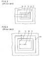
- FIG. 2 shows an example of the conventional closed gate type MOS FET in a plan view.
- FIG. 2 is a plan view of the above-mentioned configuration wherein gate electrode 11 is formed as a closed gate electrode, thereby the drain region 12 is disposed isolated from a channel stopper region which is under an oxide region 16.
- a connection to the drain electrode region 12 is made _by forming a contact opening 13 on an insulating oxide film (not shown because of transparency) and through the opening an aluminum electrode 14 contacts the underlying drain region 12.
- Source region 15 is formed around the drain region 12 and a oxide film insulating region 16 is formed surrounding the source region 15. In the above-mentioned configuration the source region 15 only touches the channel stopper under the thick insulation film 16.
- the breakdown voltage on the side of the source electrode 15 is determined by junction-between the source electrode 15 and the channel stopper under the thick insulation film.
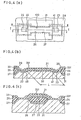
- the width W is far larger than the length L, and therefore W/L ⁇ 1. Therefore, in order to fulfill the condition W/L ⁇ 1, a MOS FET having an extremely long length L must be made. Accordingly, to fulfil the condition of W/L « 1, the channel length L must be made as long as possible as shown in FIG . 3, wherein 17 designates closed structure gate electrode of polysilicon region, 18 designates a drain diffused region, 15 designates a source diffused region, and 20 designates a .thick insulating film region under which channel stopper is formed. In the configuration of FIG.
- the configuration of FIG. 3 has such disadvantage that because of a large isolating gap space of width D the device cannot be formed in a small area with high integration.
- a high breakdown voltage performance is intended by configurating the closed gate type MOS FET for isolation of the source diffused region 15 and the- channel stopper region.
- actual designing and manufacturing of such MOS FET are difficult in an IC.
- MOS FET metal-oxide-semiconductor field-effect transistor
- a pinch off region is formed between the drain diffused region and a gate electrode,-to form an offset gate type configuration.
- MOS FET it is necessary to add one step of forming a photo mask in making process for determining a region to -make ion implantation, for forming the pinch off registered region, thereby making the manufacturing process complicated and expensive.
- MOS FET has a problem that high breakdown voltage performance is limited because it relies on pinch off register between the drain and the gate only.
- the purpose of the present invention is to provide a high breakdown voltage performance MOS FET, and a superior manufacturing method of the same.
- a MOS FET in accordance with the present invention comprises
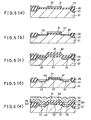
- FIG. 4(a) which is a plan view
- FIG. 4(b) which is a sectional view taken at line I-I of FIG . 4(a)
- FIG. 4(c) which is a sectional elevation view taken at line II-II of FIG. 4(a).
- the semiconductor device has, on a principal face of semiconductor substrate 31 of for instance silicon, a first conductivity type a gate electrode 21 of a polycrystalline silicon film with an insulation oxide film 33 formed inbetween.
- a source region 22 and a drain region 23 are formed on the principal face at the part on both sides of a part under the gate electrode 21, by diffusing impurities at a high implantation rate, for instance, 10 15 atoms/cm 2 of a second conductivity which is opposite to the first conductivity type. Then, a pair of pinch off resistor regions 40 and 41 are formed preferably at a lower impurity implantation rate, for instance 10 12 atoms/cm 2 , so as to extend form the source region 22 and the drain region 23, respectively, in the direction to each other. This forming of the pinch off resistor regions 40 and 41 are important feature of the present invention to achieve a high breakdown voltage. As shown in FIG. 4(b) and in FIG.
- field oxide film 26 is formed to surround the source region, drain region, pinch off region 40 and pinch off region 41 with a space of a predetermined width.
- a channel stopper 27 is formed under the field oxide film 26, and a channel part which is under the gate electrode 21 and between the pinch off resistor 40 and 41 are left as the semiconductor substrate as such.
- the channel stopper 27 In order to achieve a high breakdown voltage performance, the channel stopper 27 must be isolated from the source region 22 and drain region 23, therefore the field oxide film 26 should be formed with an isolation space from the source region 22 and the drain region 23.
- Aluminum films 28 and 29 are formed to lead out the source region 22 and the drain region 23. Insulation films 33 and 331 are formed on the field oxide film 26 and gate electrode 21. As shown by FIG. 4(a), FIG.
- the MOS semiconductor device by forming the pinch off resistor regions 40 and 41 of a lower impurity concentration than those of the source region 22 and drain region 23 and extended therefrom. And by isolating the source region 22, the drain region 23, the pinch off resistor regions 40 and 41 from the surrounding channel stopper region 27, the MOS semiconductor device can be made to have high breakdown voltage characteristic.
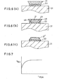
- FIG. 5 (a) , FIG. 5(b), FIG. 5(c), FIG. 5 (d) and FIG. 5(e) show manufacturing steps in accordance with the present invention.
- channel stopper 27 is formed by known ion implantation and thermal diffusion, and then field oxide film 26 is formed thereon, and subsequently silicon oxide film 33 is formed on all the substrate surface.
- polycrystalline silicon region 21 is formed at a part to form a gate electrode by chemical vapour deposition method or the like known method. Thereafter, by using a photoresist mask (not shown) the polycrystalline silicon region 21 is chemically etched to retain the part to become the gate electrode 21. Then as shown in FIG. 5(b), the silicon oxide film 33 is removed by chemical etching.
- an impurity of the second conductivity type which is of opposite conductivity type to that of the substrate, is introduced by ion implantation method using the polycrystalline silicon film 21 as mask, thereby forming impurity implanted regions 35 and 36.
- a source region 22 and the drain region 23 are formed by thermal diffusion.
- oxide silicon film 39 is formed all the surface of the wafer including the surface of polycrystalline silicon film 21, the surface of source region 22 and the surface of drain region 23.
- the surface of the wafer is subject to chemical etching or plasma etching to remove the silicon oxide film.
- oxide silicon film 331 is formed on all the surface of the wafer, then followed by chemical etching to form connection openings for the source region 22 and the drain region 23, and an aluminum film is formed and selectively etched to form electrode wirings 28 and 29, and thereafter insulation film 44 is formed as passivation film by means of chemical vapour deposition method.
- FIG. 6(a), FIG. 6(b) and FIG. 6(c) show various steps of improving the effect of the pinch off resistor regions.
- FIG. 6(a) when forming a polycrystalline silicon film to become a gate electrode 21 on a silicon oxide film 33, by utilizing silicon nitride film as etching mask formed on the polycrystalline. silicon film and using an appropriate etchant, thepolycristalline silicon film 21 can be etched in overhunging shape as shown in FIG. 6(a). Subsequently, a low temperature oxidizing treatment is carried out in a wet atomosphere, then as shown in FIG.
- the overhunging top protruding parts 46, 46 are most oxidized, and therefore the polycrystalline silicon film 21 retained unoxidized inside is shaped tapered upside narrower and bottom border as shown in FIG. 6(b).
- the low temperature oxidizing is in order not to produce unexcessive diffusion of the source region and the drain region. Since the speed of oxidation of the polycrystalline silicon film depends largely on the sheet resistance of the polychristal- line silicon film, and therefore the oxidation speed can be freely controled. Since the protruding top edge parts 46 and 46 are sufficiently supplied of oxygen, the speed at the top edge parts become faster then other parts.
- the peripheral parts of the polycrystalline film 21 are faster oxidized, thereby making the pattern of the polycrystalline silicon film as of implantation mask thereafter smaller than the original pattern of the polycrystalline silicon film. That.is the length of shrinkage of the polycrystalline silicon film pattern defines length of pinch off resistor regions 41 and 42. Therefore, length of the- shrinkage length can be controlled by controlling the overhunging chemical etching and subsequent low temperature oxidizing of the protruding top edge parts 46 and 46. The shrinkage length can be made long, and therefore the pinch off resistor regions 40 and 41 can be selected long.
- FIG. 6(c) shows a modified way of forming a long pinch off resistor region.
- a polycrystalline silicon film 21' formed on an oxide silicon film 33 on a silicon substrate 31 is etched by using an appropriate etchant to form taper etching, and a roof shaped taper etched polycrystalline film pattern is obtainable. Thereafter, by carrying out another chemical etching of the polycrystalline silicon film, the shrinked polycrystalline film pattern as of the narrower size at the tapered top face, hence a longer pinch off resistor regions are obtainable.
- the breakdown voltage becomes high for over a certain lengths of the pinch off region.
- the pinch off resistor regions are formed without requiring a special mask to define the length of the pinch off resistor regions.
- the length of the pinch off resistor regions can be controled by self-alignment method and therefore the controling is accurate and manufacturing steps become smaller.
- the impurity concentration of the pinch off resistor region is controlled small, and thereby the resistance of the pinch off resistor region can be made large, and breakdown voltage can be improved.
- the present invention can be applicable both type of the semiconductor device of n-type substrate and p-type substrate.
Landscapes
- Insulated Gate Type Field-Effect Transistor (AREA)
- Metal-Oxide And Bipolar Metal-Oxide Semiconductor Integrated Circuits (AREA)
Applications Claiming Priority (4)
| Application Number | Priority Date | Filing Date | Title |
|---|---|---|---|
| JP180896/81 | 1981-11-10 | ||
| JP56180896A JPS5882572A (ja) | 1981-11-10 | 1981-11-10 | 半導体装置の製造方法 |
| JP198118/81 | 1981-12-08 | ||
| JP56198118A JPS5898954A (ja) | 1981-12-08 | 1981-12-08 | 出力バツフア装置 |
Publications (2)
| Publication Number | Publication Date |
|---|---|
| EP0080101A2 true EP0080101A2 (de) | 1983-06-01 |
| EP0080101A3 EP0080101A3 (de) | 1985-08-07 |
Family
ID=26500261
Family Applications (1)
| Application Number | Title | Priority Date | Filing Date |
|---|---|---|---|
| EP82110291A Withdrawn EP0080101A3 (de) | 1981-11-10 | 1982-11-08 | MOS Halbleitervorrichtung |
Country Status (2)
| Country | Link |
|---|---|
| EP (1) | EP0080101A3 (de) |
| CA (1) | CA1204221A (de) |
Family Cites Families (4)
| Publication number | Priority date | Publication date | Assignee | Title |
|---|---|---|---|---|
| JPS5928992B2 (ja) * | 1975-02-14 | 1984-07-17 | 日本電信電話株式会社 | Mosトランジスタおよびその製造方法 |
| JPS5284981A (en) * | 1976-01-06 | 1977-07-14 | Mitsubishi Electric Corp | Production of insulated gate type semiconductor device |
| JPS5370768A (en) * | 1976-12-07 | 1978-06-23 | Fujitsu Ltd | Integrated circuit |
| US4280271A (en) * | 1979-10-11 | 1981-07-28 | Texas Instruments Incorporated | Three level interconnect process for manufacture of integrated circuit devices |
-
1982
- 1982-11-08 EP EP82110291A patent/EP0080101A3/de not_active Withdrawn
- 1982-11-09 CA CA000415181A patent/CA1204221A/en not_active Expired
Also Published As
| Publication number | Publication date |
|---|---|
| EP0080101A3 (de) | 1985-08-07 |
| CA1204221A (en) | 1986-05-06 |
Similar Documents
| Publication | Publication Date | Title |
|---|---|---|
| US4305200A (en) | Method of forming self-registering source, drain, and gate contacts for FET transistor structures | |
| EP0052450B1 (de) | Verfahren zur Herstellung eines Halbleiterbauelements mit polykristallinen Halbleiter- u. Metall-Elektroden | |
| US4395726A (en) | Semiconductor device of silicon on sapphire structure having FETs with different thickness polycrystalline silicon films | |
| EP0918353A1 (de) | Verfahren zur Herstellung von einem Feldeffekthalbleiterbauelement mit einem eingefügten isolierten Gatter | |
| JPS56120166A (en) | Semiconductor ic device and manufacture thereof | |
| KR930006972A (ko) | 전계 효과 트랜지스터의 제조 방법 | |
| US4271422A (en) | CMOS SOS With narrow ring shaped P silicon gate common to both devices | |
| KR890013796A (ko) | 반도체장치 및 그 제조방법 | |
| US4507846A (en) | Method for making complementary MOS semiconductor devices | |
| EP0080101A2 (de) | MOS Halbleitervorrichtung | |
| US4722912A (en) | Method of forming a semiconductor structure | |
| US4317276A (en) | Method of manufacturing an insulated gate field-effect transistor therefore in a silicon wafer | |
| JP2990784B2 (ja) | 薄膜トランジスタの製造方法 | |
| KR0151066B1 (ko) | 게이트 전극으로 티타늄 질화막을 사용하는 반도체 장치의 제조방법 | |
| JPS5538019A (en) | Manufacturing of semiconductor device | |
| JPS6229169A (ja) | Mos半導体装置の製造方法 | |
| JPH0621369A (ja) | Mos集積回路の製造方法 | |
| JPH0864688A (ja) | 半導体装置の製造方法 | |
| KR100219069B1 (ko) | 반도체장치 제조방법 | |
| JPS6211516B2 (de) | ||
| KR930001290B1 (ko) | 고 접합파괴전압을 갖는 모오스 트랜지스터 및 그 제조방법 | |
| KR890004427B1 (ko) | 고전압 고속 반도체 소자 | |
| KR100225383B1 (ko) | 반도체 소자의 제조 방법 | |
| JPS59114869A (ja) | 多結晶シリコンの浮遊ゲ−トを有する不揮発性半導体記憶装置 | |
| JPH01154561A (ja) | 半導体装置およびその製造方法 |
Legal Events
| Date | Code | Title | Description |
|---|---|---|---|
| PUAI | Public reference made under article 153(3) epc to a published international application that has entered the european phase |
Free format text: ORIGINAL CODE: 0009012 |
|
| AK | Designated contracting states |
Designated state(s): DE FR GB |
|
| PUAL | Search report despatched |
Free format text: ORIGINAL CODE: 0009013 |
|
| AK | Designated contracting states |
Designated state(s): DE FR GB |
|
| STAA | Information on the status of an ep patent application or granted ep patent |
Free format text: STATUS: THE APPLICATION IS DEEMED TO BE WITHDRAWN |
|
| 18D | Application deemed to be withdrawn |
Effective date: 19860408 |
|
| RIN1 | Information on inventor provided before grant (corrected) |
Inventor name: HOSOKAWA, YOSHIHIRO |