EP0068163A2 - Pile pour l'adresse d'instruction dans la mémoire de données d'un processeur en pipe-line - Google Patents
Pile pour l'adresse d'instruction dans la mémoire de données d'un processeur en pipe-line Download PDFInfo
- Publication number
- EP0068163A2 EP0068163A2 EP82104814A EP82104814A EP0068163A2 EP 0068163 A2 EP0068163 A2 EP 0068163A2 EP 82104814 A EP82104814 A EP 82104814A EP 82104814 A EP82104814 A EP 82104814A EP 0068163 A2 EP0068163 A2 EP 0068163A2
- Authority
- EP
- European Patent Office
- Prior art keywords
- instruction
- address
- data store
- store
- stage
- Prior art date
- Legal status (The legal status is an assumption and is not a legal conclusion. Google has not performed a legal analysis and makes no representation as to the accuracy of the status listed.)
- Granted
Links
- 230000004044 response Effects 0.000 claims description 86
- 238000012163 sequencing technique Methods 0.000 claims description 78
- 238000012546 transfer Methods 0.000 claims description 30
- 230000007246 mechanism Effects 0.000 claims description 22
- 238000000034 method Methods 0.000 claims description 7
- 238000001514 detection method Methods 0.000 claims description 2
- 238000013500 data storage Methods 0.000 abstract description 30
- 230000008901 benefit Effects 0.000 abstract description 8
- 230000000593 degrading effect Effects 0.000 abstract description 8
- 238000002360 preparation method Methods 0.000 abstract description 5
- 230000006870 function Effects 0.000 description 36
- 238000012545 processing Methods 0.000 description 7
- 238000010586 diagram Methods 0.000 description 6
- 230000000295 complement effect Effects 0.000 description 4
- 238000012360 testing method Methods 0.000 description 4
- 238000004364 calculation method Methods 0.000 description 2
- 230000001427 coherent effect Effects 0.000 description 2
- 235000008733 Citrus aurantifolia Nutrition 0.000 description 1
- 101000611618 Homo sapiens Photoreceptor disk component PRCD Proteins 0.000 description 1
- 102100040826 Photoreceptor disk component PRCD Human genes 0.000 description 1
- 235000011941 Tilia x europaea Nutrition 0.000 description 1
- 230000015572 biosynthetic process Effects 0.000 description 1
- 230000008859 change Effects 0.000 description 1
- 230000003247 decreasing effect Effects 0.000 description 1
- 230000003111 delayed effect Effects 0.000 description 1
- 239000004571 lime Substances 0.000 description 1
- 238000012423 maintenance Methods 0.000 description 1
- CPTIBDHUFVHUJK-NZYDNVMFSA-N mitopodozide Chemical compound C1([C@@H]2C3=CC=4OCOC=4C=C3[C@H](O)[C@@H](CO)[C@@H]2C(=O)NNCC)=CC(OC)=C(OC)C(OC)=C1 CPTIBDHUFVHUJK-NZYDNVMFSA-N 0.000 description 1
- 230000008520 organization Effects 0.000 description 1
- 230000008569 process Effects 0.000 description 1
- 230000009467 reduction Effects 0.000 description 1
Images

Classifications
-
- G—PHYSICS
- G06—COMPUTING; CALCULATING OR COUNTING
- G06F—ELECTRIC DIGITAL DATA PROCESSING
- G06F9/00—Arrangements for program control, e.g. control units
- G06F9/06—Arrangements for program control, e.g. control units using stored programs, i.e. using an internal store of processing equipment to receive or retain programs
- G06F9/30—Arrangements for executing machine instructions, e.g. instruction decode
- G06F9/38—Concurrent instruction execution, e.g. pipeline or look ahead
- G06F9/3802—Instruction prefetching
- G06F9/3804—Instruction prefetching for branches, e.g. hedging, branch folding
- G06F9/3806—Instruction prefetching for branches, e.g. hedging, branch folding using address prediction, e.g. return stack, branch history buffer
-
- G—PHYSICS
- G06—COMPUTING; CALCULATING OR COUNTING
- G06F—ELECTRIC DIGITAL DATA PROCESSING
- G06F9/00—Arrangements for program control, e.g. control units
- G06F9/06—Arrangements for program control, e.g. control units using stored programs, i.e. using an internal store of processing equipment to receive or retain programs
- G06F9/30—Arrangements for executing machine instructions, e.g. instruction decode
- G06F9/30003—Arrangements for executing specific machine instructions
- G06F9/3005—Arrangements for executing specific machine instructions to perform operations for flow control
- G06F9/30054—Unconditional branch instructions
-
- G—PHYSICS
- G06—COMPUTING; CALCULATING OR COUNTING
- G06F—ELECTRIC DIGITAL DATA PROCESSING
- G06F9/00—Arrangements for program control, e.g. control units
- G06F9/06—Arrangements for program control, e.g. control units using stored programs, i.e. using an internal store of processing equipment to receive or retain programs
- G06F9/30—Arrangements for executing machine instructions, e.g. instruction decode
- G06F9/38—Concurrent instruction execution, e.g. pipeline or look ahead
- G06F9/3885—Concurrent instruction execution, e.g. pipeline or look ahead using a plurality of independent parallel functional units
- G06F9/3889—Concurrent instruction execution, e.g. pipeline or look ahead using a plurality of independent parallel functional units controlled by multiple instructions, e.g. MIMD, decoupled access or execute
-
- G—PHYSICS
- G06—COMPUTING; CALCULATING OR COUNTING
- G06F—ELECTRIC DIGITAL DATA PROCESSING
- G06F9/00—Arrangements for program control, e.g. control units
- G06F9/06—Arrangements for program control, e.g. control units using stored programs, i.e. using an internal store of processing equipment to receive or retain programs
- G06F9/44—Arrangements for executing specific programs
- G06F9/448—Execution paradigms, e.g. implementations of programming paradigms
- G06F9/4482—Procedural
- G06F9/4484—Executing subprograms
- G06F9/4486—Formation of subprogram jump address
Definitions
- the invention relates to data processing systems and more particularly to the instruction mechanism in stored program data processors.
- a computer instruction is the specification of an operation to be performed, and may include the address of one or more operands on which the operation will be performed, the address for the location of the results, and an address of the next instruction in the sequence.
- SAR sequential address register
- the program should return to the point in the original instruction sequence which was the point of departure for the branch. This is accomplished by a "return instruction.”
- the instruction address to which the program is to return must be stored at the time the branch instruction was executed.
- the last in-first out (LIFO) instruction address stack must be provided to store those return addresses:
- an instruction pipeline for a data processor in which instruction execution is carried out in a sequence of phases which include fetching the instruction from an instruction storage, computing a data storage address from the fetched instruction, accessing the data storage at the computed address- to obtain a datum operand, and then carrying out the logical or arithmetic operation on the accessed datum in accordance with the fetched instruction.
- Branch and return instruction are accommodated by providing a return address stack in the data storage, which stores the next instruction store address to be returned to after a branching operation has been completed.
- a stack register is provided in the instruction fetch stage of the pipeline which contains a duplicate of the instruction store address presently residing at the top of the instruction address stack. Then when a return instruction is encountered in the instruction fetch stage, the address of the next instruction to be returned to in the instruction storage is immediately available without interrupting the flow in the pipeline.
- a stack pointer in a stage of the pipeline between the instruction fetch stage and the data store access stage then takes advantage of unused instruction phases in the pipeline, to cause the data store access stage to read the next available instruction store address from the instruction address stack therein and load it into the stack register in preparation for the next return instruction.
- the data storage and instruction stacking function can be shared in the same data storage device which is accessed by an intermediate stage in the multiple phase instruction pipeline without degrading the performance of the pipeline.
- An instruction pipeline for a data processor in which instruction execution is carried out in a sequence of phases which include fetching the instruction from an instruction storage, computing a data storage address from the fetched instruction, accessing the data storage at the computed address to obtain a datum operand, and then carrying out the logical or arithmetic operation on the accessed datum in accordance with the fetched instruction.
- Branch and return instructions are accommodated by providing a return address stack in the data storage, which stores the next instruction store address to be returned to after a branching operation has been completed.
- a stack register is provided in the instruction fetch stage of the pipeline which contains a duplicate of the instruction store address presently residing at the top of the instruction address stack. Then when a return instruction is encountered in the instruction fetch stage, the address of the next instruction to be returned to in the instruction storage is immediately available without interrupting the flow in the pipeline.
- a stack pointer in a stage of the pipeline between the instruction fetch stage and the data store access stage,-then takes advantage of unused instruction phases in the pipeline, to cause the data store access stage to read the next available instruction store address from the instructior address stack therein and load it into the stack register in preparation for the next return instruction.
- the data storage and instruction stacking function can be shared in the same data storage device which is accessed by an intermediate stage in the multiple phase instruction pipeline without degrading the performance of the pipeline.
- the real time signal processor is a single operand general purpose processor with a 16-bit data flow and a 24- bit instruction set which is particularly adapted to implement signal processing algorithms.
- the RSP has a pipelined instruction organization designed to achieve maximum processing throughput without requiring high performance, high power circuits.
- the architecture contains a full repertoire of arithmetic, logic, and control instructions including a variable precision multiply and a 32-bit divide.
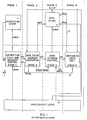
- the entire processor, exclusive of the memory, is designed to be implemented on a single VLSI chip 5 as shown in Figure 1.
- the RSP instruction set is built around instructions which perform arithmetic functions in one cycle (except multiply, divide, and left shift) where one of the operands can be contained in data store 8 and the other in a local register 18 as is shown in Figure 3. The result is returned to a local register.
- the four distinct functions to be performed in order to execute such an instruction are:
- phase 1 of an instruction is the instruction fetch.
- Phase 2 is the effective address generation.
- Phase 3 is the data memory access, and
- Phase 4 is the arithmetic function execution.
- the distinct area of hardware which implements a function is referred to as a stage.
- the hardware stages execute the four phases for four different instructions concurrently.
- RSP Since the RSP was designed to be built on a single LSI chip 5, space on the chip is at a premium. The large storage functions of data storage 8 and instruction storage 6 are therefore carried out by separate memory chips which are accessed by the RSP chip 5.
- the placement of the return address LIFO storage function in the data store 8 appeared to be unsuitable because a return address could not be accessed from the data store until two phases after the return instruction was read by the first stage, without degrading pipeline throughput.
- the address sequencing control includes a 64 level stack 10 shown in Figure 5, located in data store 8 (memory locations 0 to 63). The value written into the 'top' of the stack 10, is also held in a single 16-bit hardware stack register 18 located in the instruction sequencing and fetch stage 1.
- This 64 level stack 10 which is addressed with a 6-bit stack pointer (SP) 28 allows nesting up to 64 levels of subroutine and interrupt routines.
- the instructions which affect the stack are: branch and stack unconditionally 'BS,' return RET,' and return and enable interrupts 'RET ENABLE.' Unmasked interrupts also affect the stack.
- the updated stack pointer register 28 always contains the address of the 'top' of the data store stack 10.
- the 'RET' type instructions cause the contents of the address pointed to by the stack pointer 28 (i.e., 'top' of stack) to be used as the address of the next instruction.
- SP the stack . pointer 28
- Phase 3 of the instruction that value is read from the data store stack 10 and loaded into the stack register 18 at the end of Phase 3 of the 'RET' type instruction.
- This allows the return address just read from the data store stack 10 to be available for use by a subsequent 'RET' type instruction occurring at least one instruction away from any previous 'RET' type instruction. This is because the first 'RET' type instruction which reads the data store stack 10 and loads the value into the stack register 18 during its Phase 3, will have had time to complete this stack register update.
- the RSP chip 5 has a 64 address stack 10 immediately available to its instruction fetch stage 1 without occupying excessive chip area on the LSI device. This is achieved by employing the otherwise unused second and third stages 2 and 3 of the RSP instruction pipeline during branch and return operations to access the'stack 10 which is actually located in a partitioned area of the data store 8.
- a stored program data processor is formed on an integrated circuit chip 5, having a pipelined instruction mechanism including four time-sequential stages with a first stage 1 for instruction sequencing and fetch, a second stage 2 for data store address generation, a third stage 3 for data store access, and a fourth stage 4 for arithmetic execution. These stages operate in an overlapped mode on successive instructions each including an op code and an operand, which are accessed from an instruction store 6 external to the chip 5, to carry out arithmetic operations on data accessed from a data store 8 external to the chip 5.
- a last-in-first-out instruction address stack 10 of Figure 5 is in a partitioned area of data store 8, for storing addresses for the instruction store 6.
- An instruction address multiplexer 12 of Figure 3 is in the first stage 1 and has an output 13 connected to an address input of the instruction store 6 and having a plurality of inputs, for inputting instruction addresses to the instruction store 6.
- An instruction address incrementer 14 of Figure 3 is in the first stage 1 and has an input connected to the output 13 of the multiplexer 12 and an output connected through a sequential address register (SAR) 16 to one of the inputs of the multiplexer 12, for sequentially incrementing the instruction store addresses by unity.
- SAR sequential address register
- a stack register 18 of Figure 3 is in the first stage 1 and has an input selectively connected to either an output of the sequential address register 16 or to an output 17 from the instruction address stack 10 in the data store 8, for storing the last instruction store address outputted from the incrementer 14 or storing the last instruction store address outputted over line 17 from the instruction address stack 10 in the data store 8 and has an output selectively connected to either an input to the multiplexer 12 or to an input over line 19 to the instruction address stack 10 in the data store 8.
- Stack register 18 stores only a single address.
- An instruction sequencing decoder (sequencing controls) 20 of Figure 3 is in the first stage 1 and has an input connected to an output 7 of the instruction store 6 and an output 21 connected to the multiplexer 12, for selectively controlling the connection of the instruction store 6 address input 13, through the multiplexer 12, to either the sequential address register 16 output or to the stack register 18 output in response to the op code of the last instruction word accessed from the instruction store 6 over line 7.
- the multiplexer 12 can have one of its plurality of inputs connected to the output 7 of the instruction store 8 for selectively transferring the operand of the last instruction accessed therefrom as an unconditional branch address input to the instruction store 6 in response to the decoding of the associated op code in the instruction sequencing decoder 20.
- a data store accessing decoder 22 of Figure 4 is in the second stage 2 and has an input 7 connected to the instruction store 6 output, for decoding the op code from the last instruction accessed from the instruction store 6.
- a data store address generator 24 of Figure 4 is in the second stage 2 and has an input 7 connected to the instracier store 6 output, a control input 25 connected to the data store accessing decoder 22, and an output 26, for selectively generating a data store 8 address from the operand of. the last accessed instruction word in response to the decoding of the associated op code in the data store accessing decoder 22.
- a stack pointer 28 of Figure 4 is in the second stage 2 and has a control input 25 connected to the data store accessing decoder 22 and an output 29, for selectively incrementing or decrementing a data store address value for accessing the last instruction address stored in the instruction address stack 10 in the data store 8.
- a data store address register 30 of.Figure 5 is in the third stage 3, and has an input connected to the data store address generator 24 output 26 and to the stack pointer 28 output 29, and an output 31 connected to the address input of the data store 8, for accessing a location in the data store 8.
- the instruction sequencing decoder 20 selectively controls the transfer of the operand of an unconditional branch instruction through the multiplexer-12 to the address input 13 of the instruction store 6 in response to the associated branch op code, selectively controls the incrementing of the sequential address register 16 by unity and loads the contents thereof into the stack register 18 in response to the associated branch op code, and selectively controls the nondestructive outputting of the contents of the stack register 18 over line 19 to the data input 32 of the data store 8 in response to the associated branch op code.
- the data store accessing decoder 22 in response to the branch op code, selectively controls the incrementing of the stack pointer 28 by unity and the outputting of its contents to the data store address register 30 as the address of the location in the instruction address stack 10 for storing the contents of the stack register 18 as the_return address from the branch specified in the branch op code.
- the instruction sequencing decoder 20 in the first stage 1 carries out its controlling operations during a first phase or interval upon the occurrence of the branch instruction.
- the data store accessing decoder 22 in the second stage 2 carries out its controlling operations during a second phase following the first phase.
- the data store address register 30 in the third stage 3 accesses the data store 8 at the location in the instruction address stack 10 and the data store 8 stores the contents of the stack register 18 there, during a third phase following the second phase. In this manner, the otherwise unused second and third stages 2 and 3 are employed during a branching operation to access the instruction stack 10 which is not located on the integrated circuit chip 5.
- the instruction sequencing decoder 20 in the first stage I selectively controls the transfer of the contents of the stack register 18 through the multiplexer 12 to the address input 13 of said instruction store 6 in response to a return instruction.
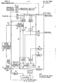
- This stage 1 shown in Figure 3 implements only Phase 1 of the instruction execution.
- the 8-bit op code of the previous instruction is decoded, the address of the current instruction is determined based on the Condition Codes in the processor and the decode of the previous instruction op code, and the current instruction is fetched from Instruction Store 6.
- the value of the Program Counter (i.e. the current instruction address) is selected from either the next sequential address 16 or one of a number of possible branch addresses.
- the address selection is under program and/or interrupt control. In all cases, the address of the current instruction is entirely resolved during Phase 1 of an instruction execution in order that branching can occur in one instruction cycle.
- the effective Data Store address is calculated for those instructions which require data memory 8 access.
- the 16-bit operand field 'a' of the instruction is passed to the Address Generation Stage 2 shown in Figure 4.
- the effective address for the Data Store operation is then formed as one of four functions depending on the instruction.
- the four types of effective address are:
- a number of instructions are provided for updating the registers that are used in the formation of the effective address (i.e. Xl, X2, Wl, and W2). These instructions complete execution in the Second Phase unless they involve Data Store operations. Data Store writes are completed in the third phase. Operations which read Data Store 8 perform the read operation and Stage 2 register update in Phase 3 so that the updated registers are available in the following phase (cycle). For Data Store operations, the effective addresses are generated by the Stage 2 logic and passed to the Data Store Address Register (DSAR) 30 at the end of Phase 2, in preparation for access in Phase 3.
- DSAR Data Store Address Register
- Phase 3 of an instruction execution the Data Store 8 is accessed at the effective address.
- the Address Generation Stage hardware 2 passes the effective address, calculated in the previous cycle (phase), to the Data Store Stage 3 of Figure 5 for use in the present phase.
- the Data Store output is loaded into the appropriate register specified by the op code of the previous instruction. This is done at the completion of Phase 3 of that instruction in preparation for use during Phase 4.
- Some instructions do not access Data Store 8 fc an operand but require the immediate operand to participate in the arithmetic of Phase 4.
- the-Data Storage Stage forms a conduit for passage of the instruction operand 'a' from the Stage 2 hardware to the Stage 4 hardware for use during Phase 4 of the instruction.
- the Arithmetic Stage 4 executes the actual arithmetic operation defined in the instruction. Most instructions in the set of arithmetic operations, execute in a single cycle of the Arithmetic Stage 4. However, the multiply, divide, and arithmetic left shift, instructions require multiple executions of this stage in order to complete. The multiply instruction requires up to 8 cycles, the divide requires 17 cycles, and the left shift instruction requires 1 more cycle (in Phase 4) than the shift count (0 to 31). In these cases, the first three stages/phases 1, 2, and 3 of the instruction execution are "frozen" while Stage 4 for the present instruction is allowed to execute until the instruction is completed.
- the functions of the I/O stage 34 can be divided into 2 major areas: Direct I/O, and Externally Controlled I/O.
- RSP Real Time Clock
- Maintenance Interface with the capability to allow a Scan In/Scan Out of all registers and latches in the RSP
- I/O Interface with the capability to allow an External Device to control the RSP by issuing a set of Function Commands.
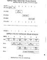
- Example 1 shows a single instruction being executed. Phases 1 through 4 refer to the four functions performed on the instruction by the four hardware stages. The cycles refer to machine cycles.
- This example illustrates the instruction 'AZ Z,a(Ml)' which adds the contents of the Masked Memory location M(a,Xl,B) to the contents of the Z register and places the sum into the Z Register.
- Example 2 shows a set of instructions which perform the following sequence of operations:
- a no-operation instruction 'NOP' is inserted in the instruction pipeline in order to allow time for the fourth stage 4 of the pipeline to complete for the 'AZ' instruction before the third stage of the 'STZ' instruction performs the storage operation to move the result.
- the unused cycles retain their position in the instruction pipeline.
- This section describes in detail the operation of the hardware stages of the RSP. It includes the details of (1) How the instructions are fetched and decoded, (2) How the effective address is generated and used, and (3) How the various Condition Codes and registers (SAR, STACK, etc.) are set and interpreted.
- This stage is depicted in the flow diagram of Figure 3. It implements the Phase 1 function of execution of the instruction pipeline.
- This Stage contains the Instruction Address Selection Logic which controls the Instruction Store 6.
- the Instruction Store 6 which is 24 bits wide, is made up of an 8-bit op code field and a 16-bit operand field. It is addressed by the Program Counter (PC) multiplexer 12.
- the PC Mux output 13 which is 16 bits, is capable of addressing an Instruction Store 6 of up to 65536 instructions.
- the Instruction Address Selection Logic decodes the 8-bit op code from the previous instruction to determine the source for the address of the present instruction. The address is selected by the PC Mux 12 and the instruction is accessed. Op codes from the previous instruction which call out Branch, Proceed, or Return, operations cause the-address of the instruction being fetched to be taken from one of five branch sources. All other op codes cause the current instruction address to be taken from the Sequential Address Register (SAR) 16 which contains the address of the last instruction fetched (PC) plus one.
- SAR Sequential Address Register
- the instruction address generation and fetch operations are performed in the same cycle to ensure that branching takes place in one cycle.
- the PC Mux 12 selects the current instruction address from among the following sources all of which are 16-bit registers.
- the Sequential Address Register (SAR) 16 is selected as the source for sequentially addressing Instruction Store 6.
- the STACK Register 18 is selected as the source for the return 'RET' type instructions.
- the Operand Field 'a' 36 of the current instruction is selected as the source for the unconditional branch instructions. It is also used for all conditional branch instructions if the conditional criterion is satisfied. Otherwise the SAR 16 is selected.
- the SAVE Register 38 is used as the source for the address of the next instruction when the proceed 'PRCD' instruction, or those functions which specify.a Proceed are used (i.e. Instructions of the form '__P_).
- the IAR/Vector 40 is only used for I/O Interrupt branches to words 1 to 63 of Instruction Store which themselves contain a Branch to the address of the appropriate Interrupt handling routine.
- Conditional branching decisions are made based on the state of the 8 condition indictors 42. These bits are set as a result of various conditions existing in the processor when the instructions are executed.
- the condition indicators include the 6 Condition Code bits generated in the Arithmetic Stage 4, and the 2 status flags generated in the other stages.
- the branch conditions are:
- Condition Codes 1 thru 5 All arithmetic instructions set Condition Codes 1 thru 5 at the end of Phase 4. For multiply, divide, and arithmetic left shift instructions which require multiple cycles of Phase 4 to complete, the Condition Codes are set after the fourth phase completes.
- the External Overflow (Condition Code 6) is determined in Phase 3 and set in Phase 4.
- the Index Compare Flag (7) is generated in the Address Generation Stage and is set in Phase 2 of its instruction execution.
- the Software Flag is set under program control in Phase 2., Condition Codes 4, 6 and 8 are latched and remain set to 1 until specifically used, at which time they are reset to 0 in Phase 2 of the branch instruction which uses them. All other Condition Code bits are set by each operation which affects them.
- conditional branch instructions are implemented in Phase 1 of the next instruction execution and therefore, are based on the conditions as they exist at that time.
- Some Branch instructions are based on Condition Codes from the Arithmetic Stage 4. These branches are based on the conditions which are set as a result of arithmetic instructions coded three cycles prior to the Branch or earlier.
- the Branch on Index Compare Flag (BICF) is based on a condition set as a result of some previous Overflow instruction is based on a condition set 3 cycles or more prior to the branch instruction.
- the address sequencing control includes a 64 level Stack 10 located in Data Store 8 (memory locations 0 to 63). The value written into the 'Top' of the Stack 10, is also held in a single 16-bit hardware Stack Register 18 located in the Instruction Sequencing & : Fetch Stage 1.
- This 64 level Stack 10 which is addressed with a 6-bit Stack Pointer (SP) 28 allows nesting up to 64 levels of Subroutine and Interrupt routines.
- SP Stack Pointer
- the instructions which affect the Stack 10 are: Branch and Stack unconditionally 'BS', Return 'RET', and Return and Enable Interrupts 'RET ENABLE'. Unmasked Interrupts also affect the Stack 10.
- SP Stack Pointer
- the 'PET' type instructions cause the contents of the address pointed to by the Stack Pointer 28 (i.e. 'Top' of Stack) to be used as the address of the next instruction. Since this value is held in the Stack Register 18, it is available for use in the next cycle.
- the decoder 20 must insert a NO-OP signal on line 7 in place of the normal return instruction in Phases 2, 3, and 4 of the second fetch of the second 'RET' type instruction so that the decoder 22 will inhibit the Stack Pointer 28 from getting updated a second time and decoder 75 will inhibit the reading of data store 8 a second time.
- the result of this hardware generated NO-OP operation will be that the first fetch of the second 'RET' type instruction will operate normally, but the second fetch of the second 'RET' type instruction will operate as normal in Phase 1 and behave as a 'NOP' instruction in Phases 2, 3, and 4.
- a third consecutive 'RET' type instruction will be treated like the first since it follows an effective 'NOP' rather than an 'RET' type instruction.
- the operation with two or more consecutive return instructions is as follows.
- the value stored in the stack register 18 will be S . and the value stored in the stack pointer 28 will be i.
- the instruction sequencing decoder 20 in the first stage 1 decodes a previous instruction during the first cycle, and controls the multiplexer 12 to input on line 13, a first address to the instruction store 6, fetching a first instruction from the instruction store 6.
- the stack register 18 is storing S . and the stack pointer 28 is storing i.
- the instruction sequencing decoder 20 in the first stage 1 decodes the first instruction as a first return instruction during the second cycle following the first cycle, and controls the multiplexer 12 to transfer the contents S i of the stack register 18 as a second address to the instruction store 6, fetching a second instruction from the instruction store 6.
- the data store accessing decoder 22 in the second stage 2 decodes the first instruction as the first return instruction during the second cycle and controls the stack pointer 28 to decrement its contents by unity to a value i-1 which is output to the data store address register 30 in the third stage 3 as a first data store 8 address for the instruction address stack 10.
- the stack register 18 is storing Si and the stack pointer 28 is storing i-1.
- the instruction sequencing decodes 20 in the first stage 1 decodes the second instruction as a second return instruction during the third cycle following the second cycle, and controls the multiplexer 12 to again transfer the contents S i which still occupies the stack register 18, as the second address to the instruction store 6, again fetching the second-instruction from the instruction store 6.
- the instruction sequencing decoder 20 in the first stage 1 has a No-Op output connected via line 7 to the data store accessing decoder 22 in the second stage 2 and to the op code decoder 75 in the third stage 3, for outputting a No-Op signal on line 7 upon the detection of the second return instruction during the third cycle.
- the data store accessing decoder 22 in the second stage 2 decodes the second instruction as the second return instruction during the third cycle and controls the stack pointer 28 to decrement its contents by unity to a value i-2 which is output to the data store address register 30 in the third stage 3 as a second data store 8 address for the instruction address stack 10.
- the op code decoder 75 in ; the third stage 3 decodes the first instruction as the first return instruction during the third cycle and controls the data store 8 to access a first datum from the instruction address stack 10 at the first data store address i-1 and output the first datum as the value S i-1 to the stack register 18 over line 17 in the first stage 1.
- the stack register 18 is storing S i-1 and the stack pointer 28 is storing i-2.
- the instruction'sequencing decoder 20 in the first stage I again decodes the second instruction as the second occurrence of the second return instruction during the fourth cycle following the third cycle, and controls the multiplexer 12 to transfer the contents S i-1 of the stack register 18 as a third address to the instruction store 6, fetching a third instruction from the instruction store 6.
- the data accessing decoder 22 in the second stage 2 omits operations on the stack pointer 28 during the fourth cycle, in response to the No-Op signal on line 7.
- the op code decoder 75 in the third stage 3 decodes the second instruction as the second return instruction during the fourth cycle and controls the data store 8 to access a second datum from the instruction address stack 10 at the second data store address i-2 and output the second datum as the value S i-2 to the stack register 18 over line 19 in the first stage 1.
- the stack register 18 is storing S i-2 and the stack ponter 28 is storing i-2.
- the instruction sequencing decoder 20 in the first stage 1 decodes the third instruction as a first next instruction during the fifth cycle following the fourth cycle, and controls the multiplexer 12 to input a first next instruction address to the instruction store 6, fetching a fourth instruction from the instruction store 6.
- the data store accessing decoder 22 in the second stage 2 decodes the third instruction as the first next instruction during the fifth cycle, and controls the data store address generator 24 to output a first next data store address to the data store address register 30 in the third stage 3.
- the op code decoder 75 in the third stage 3 omits operations on the data store 8 during the fifth cycle, in response to the No-Op signal on line 7.
- the contents of the stack register 18 and stackpointer 28 do not change for the sixth machine cycle, in this example.
- the instruction sequencing decoder 20 in the first stage 1 decides the fourth instruction as a second next instruction during the sixth cycle following the fifth cycle, and controls the multiplexer 12 to input a second next instruction address to the instruction store 6, fetching a fifth instruction from the instruction store 6.
- the data store accessing decoder 22 in the second stage 2 decodes the fourth instruction as the second next instruction during the sixth cycle, and controls the data store address generator 24 to output a second next data store address to the data store address register 30 in the third stage 3.
- the op code decoder 75 in the third stage 3 decodes the third instruction or the first next instruction during the sixth cycle and controls the data store 8 to access a third datum at the first next data store address. In this manner, the instruction store accessing operations for two consecutive return instructions are expanded in time.
- the Interrupt causes a branch to the appropriate Interrupt Entry Address in Instruction Store 6.
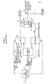
- This Stage 2 of Figure 4 implements the second Phase of the instruction execution.
- the primary function of the Address Generation Stage 2 is to calculate the Effective Address for Data Store 8 operations which take place in the third phase of the instruction execution. Additional functions which are implemented here are as follows:
- FIG. 4 shows the functional flow diagram for this stage. All control registers in this stage (except the Stack Pointer 28), are 16 bits in length. The Stack Pointer 28 is 6 bits long. The following table lists these control registers with their associated names.
- Adder 1 is a 16 bit 2 t s complement adder with additional logic to develop the greater than and less than or equal to functions. Adder 1 can form the complement of a value on the right input for subtraction. Separate control over the carry into the LSB is provided. This allows the adder to perform 2's complement arithmetic or to insert a 1 bit offset which is used in the compare function to create the "Less than or Equal" function. Adder 2 is also a 16 bit 2's complement adder.
- the interfaces to the address generation logic are:
- the generation of the Effective Data Store Address on line 26 involves the implementation of one of the four forms of the address specification. The four forms were previously described. All Effective Addresses are available at the end of Phase 2 of the instruction execution. They are passed to the Data Store Stage 3 for use in Phase 3.
- Index Register Testing An Index Compare Flag (ICF) is generated from the results of Adder 1 and is used by the conditional Branch instruction 'BICF'.
- the adder compares the selected Index Register with either the operand field 'a' or the selected 'W' Register, by performing a subtract of the immediate value (or the appropriate 'W' Register) from the appropriate Index Register, without affecting the contents of the Index Register.
- the flag is set to the result of the test specified (>, >, ⁇ , ⁇ ). This test takes place during Phase 2 of the instruction execution, and the compare flag is set at the end of Phase 2.
- a 'BICF' instruction which branches on the result of this compare, will be effective if coded on the next instruction.
- SAVE Register Calculation The feedback path from Adder 1 to the Index Registers is also made available to the SAVE Register 38.
- the SAVE Register is loaded at the end of Phase 2. This function is implemented by the ASV instruction.
- Index Register/Storage Interface The index Registers interface to Data Store either directly or via the 'V' Register.
- the interface to the 'V' Register allows data to be temporarily held there (or loaded from there) if desired.
- Reads of Data Store 8 cause the Data Store contents to be latched into the appropriate Index Register at the end of Phase 3.
- Writes to Data Store occur during Phase 3.
- the Transfer (V) Register 50 is used to form-a path between Data Store 8 and all of the control'registers for the Address Generation Stage 2. This path is bi-directional, in that, data may be transferred from Data Store to any control register or from the control registers to Data Store through the 'V' Register.
- the 'V' Register can also be used as a temporary residence of data between the Data Store 8 and all of the control registers. Data is loaded from the 'V' Register to the destination register during Phase 2 of the instruction. For transfers of these control registers to the 'V' Register, an effective direct path is provided back to the 'V' Register with the transfers occurring in Phase 2.
- Reads of Data Store 8 have the contents of Data Store delivered to the register pointed to by the op code of the current instruction, at the end of Phase 3. Writes to Data Store from the 'V' Register occur during Phase 3.
- Some instructions require the operand 'a' for Phase 4 of their execution.
- the Address Generation Stage 2 is required to deliver the value 'a' to the Effective Address lines at the end of Phase 2. This value is passed through the Data Store Stage 3 in Phase 3 and.delivered to the appropriate register in the Stage 4 logic pointed to by the op code of the instruction. From there it is available in Phase 4 as required.
- the Data Store Stage 4 of Figure 5 is made up of the Data Store 8, the address select multiplexer and Data Store Address Register 30, the input selection multiplexer 54, and the output selection multiplexer.
- the Data Store Stage 3 performs the Data Store and fetch operations for the RSP.
- the Data Store 8 uses 16-bit words and is addressable up to 65536 words.
- a 16-bit address register 30 along with source selection logic is provided for selecting between the Effective Address generated by the Address Generation Stage 2 and the address provided by the I/O.
- Source selection is carried out by the op code decoder 75 which controls the multiplexer 54 and the data store address register 30 in response to op code inputs on line 7.
- the data source selection is made from the output 70 of (1) the Arithmetic Stage 4, (2) the Address Generation Stage 2 (Xl, X2, and V Registers) (3) the Stack Register 18 in the Instruction Fetch Stage 1, and (4) the I/O 34.
- the Data Store 8 output 56 is routed to the appropriate register specified by the op code of the current instruction at the completion of Phase 3, for use throughout Phase 4. Data Store Write operations take place in Phase 3 of the instruction execution using the Effective Address generated in Stage 2. The data that is stored is the data which is available in the Source Register at the end of Phase 2.
- Data Fetch operations are performed in Phase 3 of instruction execution and the data is placed in the register pointed to by the op code of the current instruction.
- the data is put in the appropriate register at the end of Phase 3, and then during Phase 4 it is passed through the adder or multiplier (thus setting Condition Codes) and written into the destination register at the end of Phase 4 of the instruction.
- I/O Input/Output logic 34 usage of Data Store 8 occurs using a Cycle Steal operation. Whenever the I/O requires a Data Store operation, the pipeline is stopped while the cycle for Data Store 8 is used by the I/O. Upon completion of a single Cycle Steal for the I/O operation, the pipeline resumes. All Stages of the pipeline must stop together in order to maintain coherent execution of the instructions.
- the resulting instruction pipeline architecture for the real time signal processor chip takes advantage of unused instruction phases during the branch and return operations, to enable the accessing of a 64 address (LIFO) Stack which is located in a partitioned area of the data store.
- LIFO 64 address
- the contents of the address stack are immediately available with the aid of the stack register in the first instruction stage.
- excessive chip area and power are not consumed by the address stack on the processor chip, which would otherwise have had to be included on the chip in order to be immediately available to the instruction fetch stage.
- the partitioned size of the address stack in the data store can be decreased and the saved area used for additional data storage.
Landscapes
- Engineering & Computer Science (AREA)
- Software Systems (AREA)
- Theoretical Computer Science (AREA)
- Physics & Mathematics (AREA)
- General Engineering & Computer Science (AREA)
- General Physics & Mathematics (AREA)
- Executing Machine-Instructions (AREA)
- Advance Control (AREA)
Applications Claiming Priority (2)
| Application Number | Priority Date | Filing Date | Title |
|---|---|---|---|
| US06/280,417 US4399507A (en) | 1981-06-30 | 1981-06-30 | Instruction address stack in the data memory of an instruction-pipelined processor |
| US280417 | 1981-06-30 |
Publications (3)
| Publication Number | Publication Date |
|---|---|
| EP0068163A2 true EP0068163A2 (fr) | 1983-01-05 |
| EP0068163A3 EP0068163A3 (en) | 1986-06-25 |
| EP0068163B1 EP0068163B1 (fr) | 1988-09-07 |
Family
ID=23072986
Family Applications (1)
| Application Number | Title | Priority Date | Filing Date |
|---|---|---|---|
| EP82104814A Expired EP0068163B1 (fr) | 1981-06-30 | 1982-06-02 | Pile pour l'adresse d'instruction dans la mémoire de données d'un processeur en pipe-line |
Country Status (4)
| Country | Link |
|---|---|
| US (1) | US4399507A (fr) |
| EP (1) | EP0068163B1 (fr) |
| JP (1) | JPS6058490B2 (fr) |
| DE (1) | DE3279007D1 (fr) |
Cited By (4)
| Publication number | Priority date | Publication date | Assignee | Title |
|---|---|---|---|---|
| EP0208181A1 (fr) * | 1985-06-28 | 1987-01-14 | Hewlett-Packard Company | File d'attente de compteur d'instructions pour processeur de type pipeline |
| EP0219203A2 (fr) * | 1985-08-30 | 1987-04-22 | Advanced Micro Devices, Inc. | Commande de calculateur avec branchement en un cycle |
| EP0247175A1 (fr) * | 1985-11-27 | 1987-12-02 | Motorola Inc | Unite de commande d'un processeur de donnees ayant un service d'interruption utilisant une reorientation de prelecture d'instructions. |
| EP0742513A2 (fr) * | 1995-05-11 | 1996-11-13 | Matsushita Electric Industrial Co., Ltd. | Processeur qui retourne rapidement de sous-programmes et appareil de traduction de programmes qui génère des programmes machines qui retournent rapidement de sous-programmes |
Families Citing this family (72)
| Publication number | Priority date | Publication date | Assignee | Title |
|---|---|---|---|---|
| NL8006163A (nl) * | 1980-11-12 | 1982-06-01 | Philips Nv | Inrichting voor het sorteren van datawoorden volgens de waarden van telkens daarbij behorende attribuutgetallen. |
| US4541045A (en) * | 1981-09-21 | 1985-09-10 | Racal-Milgo, Inc. | Microprocessor architecture employing efficient operand and instruction addressing |
| JPS58129550A (ja) * | 1982-01-27 | 1983-08-02 | Toshiba Corp | 演算制御装置 |
| JPS58189739A (ja) * | 1982-04-30 | 1983-11-05 | Hitachi Ltd | デ−タ処理システム |
| JPS592143A (ja) * | 1982-06-29 | 1984-01-07 | Hitachi Ltd | 情報処理装置 |
| US4594659A (en) * | 1982-10-13 | 1986-06-10 | Honeywell Information Systems Inc. | Method and apparatus for prefetching instructions for a central execution pipeline unit |
| US4498136A (en) * | 1982-12-15 | 1985-02-05 | Ibm Corporation | Interrupt processor |
| US4613935A (en) * | 1983-02-02 | 1986-09-23 | Couleur John F | Method and apparatus for pipe line processing with a single arithmetic logic unit |
| US4620274A (en) * | 1983-04-01 | 1986-10-28 | Honeywell Information Systems Inc. | Data available indicator for an exhausted operand string |
| JPS6015771A (ja) * | 1983-07-08 | 1985-01-26 | Hitachi Ltd | ベクトルプロセッサ |
| US4578750A (en) * | 1983-08-24 | 1986-03-25 | Amdahl Corporation | Code determination using half-adder based operand comparator |
| JPS6051948A (ja) * | 1983-08-31 | 1985-03-23 | Hitachi Ltd | 情報処理装置 |
| JPS6074034A (ja) * | 1983-09-30 | 1985-04-26 | Toshiba Corp | パイプライン制御方式 |
| JPS60107141A (ja) * | 1983-11-16 | 1985-06-12 | Fujitsu Ltd | プランチ制御方式 |
| JPS60156151A (ja) * | 1983-12-23 | 1985-08-16 | Nec Corp | メモリアクセス制御装置 |
| AU553416B2 (en) * | 1984-02-24 | 1986-07-17 | Fujitsu Limited | Pipeline processing |
| US4674032A (en) * | 1984-04-02 | 1987-06-16 | Unisys Corporation | High-performance pipelined stack with over-write protection |
| US4600986A (en) * | 1984-04-02 | 1986-07-15 | Sperry Corporation | Pipelined split stack with high performance interleaved decode |
| US4722052A (en) * | 1984-04-02 | 1988-01-26 | Sperry Corporation | Multiple unit adapter |
| JPH0776917B2 (ja) * | 1984-12-29 | 1995-08-16 | ソニー株式会社 | マイクロコンピユ−タ |
| CA1250667A (fr) * | 1985-04-15 | 1989-02-28 | Larry D. Larsen | Controle des branchements dans un processeur de signaux pipeline triphase |
| US4794517A (en) * | 1985-04-15 | 1988-12-27 | International Business Machines Corporation | Three phased pipelined signal processor |
| JPH0743648B2 (ja) * | 1985-11-15 | 1995-05-15 | 株式会社日立製作所 | 情報処理装置 |
| JPS62145326A (ja) * | 1985-12-20 | 1987-06-29 | Toshiba Corp | マイクロプログラム制御回路 |
| EP0239081B1 (fr) * | 1986-03-26 | 1995-09-06 | Hitachi, Ltd. | Processeur de données en pipeline capable de décoder et exécuter plusieurs instructions en parallèle |
| JPS62226232A (ja) * | 1986-03-28 | 1987-10-05 | Toshiba Corp | 分岐先アドレス算出回路 |
| JP2545789B2 (ja) * | 1986-04-14 | 1996-10-23 | 株式会社日立製作所 | 情報処理装置 |
| US5161217A (en) * | 1986-10-14 | 1992-11-03 | Bull Hn Information Systems Inc. | Buffered address stack register with parallel input registers and overflow protection |
| US4991090A (en) * | 1987-05-18 | 1991-02-05 | International Business Machines Corporation | Posting out-of-sequence fetches |
| US4974158A (en) * | 1987-06-10 | 1990-11-27 | Mitsubishi Denki Kabushiki Kaisha | Multiple sequentially transferrable stackpointers in a data processor in a pipelining system |
| US5179688A (en) * | 1987-06-30 | 1993-01-12 | Tandem Computers Incorporated | Queue system with uninterrupted transfer of data through intermediate locations to selected queue location |
| DE3726192A1 (de) * | 1987-08-06 | 1989-02-16 | Otto Mueller | Stacksteuerung |
| EP0312764A3 (fr) * | 1987-10-19 | 1991-04-10 | International Business Machines Corporation | Processeur de données comportant plusieurs unités d'exécution pour traiter plusieurs classes d'instructions en parallèle |
| US5197136A (en) * | 1987-11-12 | 1993-03-23 | Matsushita Electric Industrial Co., Ltd. | Processing system for branch instruction |
| US5822578A (en) * | 1987-12-22 | 1998-10-13 | Sun Microsystems, Inc. | System for inserting instructions into processor instruction stream in order to perform interrupt processing |
| KR970005453B1 (ko) * | 1987-12-25 | 1997-04-16 | 가부시기가이샤 히다찌세이사꾸쇼 | 고속처리에 적합한 데이타 처리장치 |
| US5193205A (en) * | 1988-03-01 | 1993-03-09 | Mitsubishi Denki Kabushiki Kaisha | Pipeline processor, with return address stack storing only pre-return processed address for judging validity and correction of unprocessed address |
| US5136696A (en) * | 1988-06-27 | 1992-08-04 | Prime Computer, Inc. | High-performance pipelined central processor for predicting the occurrence of executing single-cycle instructions and multicycle instructions |
| GB8817911D0 (en) * | 1988-07-27 | 1988-09-01 | Int Computers Ltd | Data processing apparatus |
| US5101341A (en) * | 1988-08-25 | 1992-03-31 | Edgcore Technology, Inc. | Pipelined system for reducing instruction access time by accumulating predecoded instruction bits a FIFO |
| US4914584A (en) * | 1988-10-17 | 1990-04-03 | Gibson Glenn A | Rules and apparatus for an intermediate code memory that buffers code segments |
| JP2858140B2 (ja) * | 1988-10-19 | 1999-02-17 | アポロ・コンピューター・インコーポレーテッド | パイプラインプロセッサ装置および方法 |
| US5099421A (en) * | 1988-12-30 | 1992-03-24 | International Business Machine Corporation | Variable length pipe operations sequencing |
| US5179691A (en) * | 1989-04-12 | 1993-01-12 | Unisys Corporation | N-byte stack-oriented CPU using a byte-selecting control for enhancing a dual-operation with an M-byte instruction word user program where M<N<2M |
| US6807609B1 (en) | 1989-12-04 | 2004-10-19 | Hewlett-Packard Development Company, L.P. | Interleaving read and write operations on a bus and minimizing buffering on a memory module in a computer system |
| US5179673A (en) * | 1989-12-18 | 1993-01-12 | Digital Equipment Corporation | Subroutine return prediction mechanism using ring buffer and comparing predicated address with actual address to validate or flush the pipeline |
| US5251306A (en) * | 1990-01-16 | 1993-10-05 | Advanced Micro Devices, Inc. | Apparatus for controlling execution of a program in a computing device |
| JPH0437927A (ja) * | 1990-06-01 | 1992-02-07 | Sony Corp | プロセッサの処理方法 |
| JP3288372B2 (ja) * | 1990-06-11 | 2002-06-04 | クレイ、リサーチ、インコーポレーテッド | 命令スケジューリング最適化方法 |
| US5202975A (en) * | 1990-06-11 | 1993-04-13 | Supercomputer Systems Limited Partnership | Method for optimizing instruction scheduling for a processor having multiple functional resources |
| US5655096A (en) * | 1990-10-12 | 1997-08-05 | Branigin; Michael H. | Method and apparatus for dynamic scheduling of instructions to ensure sequentially coherent data in a processor employing out-of-order execution |
| US5459845A (en) * | 1990-12-20 | 1995-10-17 | Intel Corporation | Instruction pipeline sequencer in which state information of an instruction travels through pipe stages until the instruction execution is completed |
| JP3211423B2 (ja) * | 1992-10-13 | 2001-09-25 | ソニー株式会社 | 分岐命令実行方法および分岐命令実行装置 |
| JP3345787B2 (ja) * | 1993-04-13 | 2002-11-18 | 三菱電機株式会社 | データ処理装置 |
| GB2281986B (en) * | 1993-09-15 | 1997-08-06 | Advanced Risc Mach Ltd | Data processing reset |
| US5623614A (en) * | 1993-09-17 | 1997-04-22 | Advanced Micro Devices, Inc. | Branch prediction cache with multiple entries for returns having multiple callers |
| US5724566A (en) * | 1994-01-11 | 1998-03-03 | Texas Instruments Incorporated | Pipelined data processing including interrupts |
| US5774712A (en) * | 1996-12-19 | 1998-06-30 | International Business Machines Corporation | Instruction dispatch unit and method for mapping a sending order of operations to a receiving order |
| US6317796B1 (en) * | 1997-10-06 | 2001-11-13 | Sun Microsystems, Inc. | Inline database for receiver types in object-oriented systems |
| US6009517A (en) | 1997-10-06 | 1999-12-28 | Sun Microsystems, Inc. | Mixed execution stack and exception handling |
| US5958039A (en) * | 1997-10-28 | 1999-09-28 | Microchip Technology Incorporated | Master-slave latches and post increment/decrement operations |
| FR2770660B1 (fr) * | 1997-11-03 | 2000-08-25 | Inside Technologies | Microprocesseur, notamment pour carte a puce |
| US6044460A (en) * | 1998-01-16 | 2000-03-28 | Lsi Logic Corporation | System and method for PC-relative address generation in a microprocessor with a pipeline architecture |
| US5974543A (en) * | 1998-01-23 | 1999-10-26 | International Business Machines Corporation | Apparatus and method for performing subroutine call and return operations |
| US7032100B1 (en) | 1999-12-17 | 2006-04-18 | Koninklijke Philips Electronics N.V. | Simple algorithmic cryptography engine |
| US6910119B1 (en) * | 2000-06-21 | 2005-06-21 | Intel Corporation | Instruction pipe and stall therefor to accommodate shared access to return stack buffer |
| US6633969B1 (en) | 2000-08-11 | 2003-10-14 | Lsi Logic Corporation | Instruction translation system and method achieving single-cycle translation of variable-length MIPS16 instructions |
| US7546451B1 (en) | 2002-06-19 | 2009-06-09 | Finisar Corporation | Continuously providing instructions to a programmable device |
| TWI289751B (en) * | 2003-02-27 | 2007-11-11 | Mediatek Inc | Method for increasing memory in a processor |
| JP5613894B2 (ja) * | 2008-08-11 | 2014-10-29 | 日本電産サンキョー株式会社 | 非接触icカードリーダ及びデータ読取方法 |
| US20100221528A1 (en) * | 2009-02-27 | 2010-09-02 | Schwab Thomas J | Extrusion coated article |
| US8813018B1 (en) * | 2012-10-05 | 2014-08-19 | Altera Corporation | Method and apparatus for automatically configuring memory size |
Citations (2)
| Publication number | Priority date | Publication date | Assignee | Title |
|---|---|---|---|---|
| US4041462A (en) * | 1976-04-30 | 1977-08-09 | International Business Machines Corporation | Data processing system featuring subroutine linkage operations using hardware controlled stacks |
| US4236206A (en) * | 1978-10-25 | 1980-11-25 | Digital Equipment Corporation | Central processor unit for executing instructions of variable length |
Family Cites Families (14)
| Publication number | Priority date | Publication date | Assignee | Title |
|---|---|---|---|---|
| NL273031A (fr) * | 1960-12-30 | |||
| US3740728A (en) * | 1972-01-19 | 1973-06-19 | Hughes Aircraft Co | Input/output controller |
| US3900834A (en) * | 1972-09-05 | 1975-08-19 | Bunker Ramo | Memory update apparatus utilizing chain addressing |
| US3840861A (en) * | 1972-10-30 | 1974-10-08 | Amdahl Corp | Data processing system having an instruction pipeline for concurrently processing a plurality of instructions |
| US4068304A (en) * | 1973-01-02 | 1978-01-10 | International Business Machines Corporation | Storage hierarchy performance monitor |
| US3875391A (en) * | 1973-11-02 | 1975-04-01 | Raytheon Co | Pipeline signal processor |
| US3984817A (en) * | 1973-11-08 | 1976-10-05 | Honeywell Information Systems, Inc. | Data processing system having improved program allocation and search technique |
| US4025771A (en) * | 1974-03-25 | 1977-05-24 | Hughes Aircraft Company | Pipe line high speed signal processor |
| GB1467726A (en) * | 1974-05-02 | 1977-03-23 | Solartron Electronic Group | Interfaces for data transmission systems |
| US3935563A (en) * | 1975-01-24 | 1976-01-27 | The United States Of America As Represented By The Secretary Of The Navy | Computer footprint file |
| US4016543A (en) * | 1975-02-10 | 1977-04-05 | Formation, Inc. | Processor address recall system |
| DE2555963C2 (de) * | 1975-12-12 | 1982-10-28 | Ibm Deutschland Gmbh, 7000 Stuttgart | Einrichtung zur Funktionsmodifizierung |
| GB1506972A (en) * | 1976-02-06 | 1978-04-12 | Int Computers Ltd | Data processing systems |
| GB1527289A (en) * | 1976-08-17 | 1978-10-04 | Int Computers Ltd | Data processing systems |
-
1981
- 1981-06-30 US US06/280,417 patent/US4399507A/en not_active Expired - Lifetime
-
1982
- 1982-04-20 JP JP57064838A patent/JPS6058490B2/ja not_active Expired
- 1982-06-02 DE DE8282104814T patent/DE3279007D1/de not_active Expired
- 1982-06-02 EP EP82104814A patent/EP0068163B1/fr not_active Expired
Patent Citations (2)
| Publication number | Priority date | Publication date | Assignee | Title |
|---|---|---|---|---|
| US4041462A (en) * | 1976-04-30 | 1977-08-09 | International Business Machines Corporation | Data processing system featuring subroutine linkage operations using hardware controlled stacks |
| US4236206A (en) * | 1978-10-25 | 1980-11-25 | Digital Equipment Corporation | Central processor unit for executing instructions of variable length |
Non-Patent Citations (2)
| Title |
|---|
| IBM TECHNICAL DISCLOSURE BULLETIN, vol. 22, no. 8B, January 1980, pages 3775-3777, New York, US; J.A. KISELAK et al.: "Microprogram link/return mechanism" * |
| IBM TECHNICAL DISCLOSURE BULLETIN, vol. 24, no. 7A, December 1981, pages 3255-3258, New York, US; J. LOSQ: "Subroutine return address stack" * |
Cited By (8)
| Publication number | Priority date | Publication date | Assignee | Title |
|---|---|---|---|---|
| EP0208181A1 (fr) * | 1985-06-28 | 1987-01-14 | Hewlett-Packard Company | File d'attente de compteur d'instructions pour processeur de type pipeline |
| EP0219203A2 (fr) * | 1985-08-30 | 1987-04-22 | Advanced Micro Devices, Inc. | Commande de calculateur avec branchement en un cycle |
| EP0219203A3 (en) * | 1985-08-30 | 1989-07-19 | Advanced Micro Devices, Inc. | Computer control providing single-cycle branching |
| EP0247175A1 (fr) * | 1985-11-27 | 1987-12-02 | Motorola Inc | Unite de commande d'un processeur de donnees ayant un service d'interruption utilisant une reorientation de prelecture d'instructions. |
| EP0247175A4 (fr) * | 1985-11-27 | 1988-03-22 | Motorola Inc | Unite de commande d'un processeur de donnees ayant un service d'interruption utilisant une reorientation de prelecture d'instructions. |
| EP0742513A2 (fr) * | 1995-05-11 | 1996-11-13 | Matsushita Electric Industrial Co., Ltd. | Processeur qui retourne rapidement de sous-programmes et appareil de traduction de programmes qui génère des programmes machines qui retournent rapidement de sous-programmes |
| EP0742513A3 (fr) * | 1995-05-11 | 1997-03-19 | Matsushita Electric Ind Co Ltd | Processeur qui retourne rapidement de sous-programmes et appareil de traduction de programmes qui génère des programmes machines qui retournent rapidement de sous-programmes |
| US6170998B1 (en) * | 1995-05-11 | 2001-01-09 | Matsushita Electric Industrial Co., Ltd. | Processor which returns from a subroutine at high speed and a program translating apparatus which generates machine programs that makes a high-speed return from a subroutine |
Also Published As
| Publication number | Publication date |
|---|---|
| JPS6058490B2 (ja) | 1985-12-20 |
| US4399507A (en) | 1983-08-16 |
| EP0068163B1 (fr) | 1988-09-07 |
| JPS585847A (ja) | 1983-01-13 |
| EP0068163A3 (en) | 1986-06-25 |
| DE3279007D1 (en) | 1988-10-13 |
Similar Documents
| Publication | Publication Date | Title |
|---|---|---|
| EP0068163B1 (fr) | Pile pour l'adresse d'instruction dans la mémoire de données d'un processeur en pipe-line | |
| US5261113A (en) | Apparatus and method for single operand register array for vector and scalar data processing operations | |
| US4449184A (en) | Extended address, single and multiple bit microprocessor | |
| US5664215A (en) | Data processor with an execution unit for performing load instructions and method of operation | |
| US4587632A (en) | Lookahead stack oriented computer | |
| US5954815A (en) | Invalidating instructions in fetched instruction blocks upon predicted two-step branch operations with second operation relative target address | |
| US4740893A (en) | Method for reducing the time for switching between programs | |
| US5440747A (en) | Data processor with control logic for storing operation mode status and associated method | |
| EP0213842A2 (fr) | Mécanisme de recherche de données en mémoire en parallèle avec l'exécution d'instructions dans un processeur à jeu d'instructions réduit | |
| US4713750A (en) | Microprocessor with compact mapped programmable logic array | |
| JPH0731603B2 (ja) | Forth特定言語マイクロプロセサ | |
| EP0365188A2 (fr) | Méthode et dispositif pour code de condition dans un processeur central | |
| EP0476722B1 (fr) | Système de traitement de données | |
| JPH0517588B2 (fr) | ||
| US4323964A (en) | CPU Employing micro programmable control for use in a data processing system | |
| US5097407A (en) | Artificial intelligence processor | |
| EP0772819B1 (fr) | Appareil et procede pour determiner avec efficacite des adresses pour les donnees presentant une erreur d'alignement en memoire | |
| EP0954791B1 (fr) | Microcontroleur huit bits a architecture risc | |
| EP0130381A2 (fr) | Mécanisme pour la réalisation d'instructions d'aiguillage sur n'importe quel bit dans n'importe quel registre exécutable en un cycle de machine dans un système ordinateur à jeu d'instructions primitif | |
| US5771366A (en) | Method and system for interchanging operands during complex instruction execution in a data processing system | |
| US5034879A (en) | Programmable data path width in a programmable unit having plural levels of subinstruction sets | |
| EP0079370B1 (fr) | Ordinateur numerique pouvant executer des instructions en trois parties multiplexees dans le temps | |
| US6161171A (en) | Apparatus for pipelining sequential instructions in synchronism with an operation clock | |
| EP0226991B1 (fr) | Dispositif de traitement de données | |
| US4975837A (en) | Programmable unit having plural levels of subinstruction sets where a portion of the lower level is embedded in the code stream of the upper level of the subinstruction sets |
Legal Events
| Date | Code | Title | Description |
|---|---|---|---|
| PUAI | Public reference made under article 153(3) epc to a published international application that has entered the european phase |
Free format text: ORIGINAL CODE: 0009012 |
|
| AK | Designated contracting states |
Designated state(s): DE FR GB |
|
| 17P | Request for examination filed |
Effective date: 19830420 |
|
| PUAL | Search report despatched |
Free format text: ORIGINAL CODE: 0009013 |
|
| AK | Designated contracting states |
Kind code of ref document: A3 Designated state(s): DE FR GB |
|
| 17Q | First examination report despatched |
Effective date: 19870325 |
|
| GRAA | (expected) grant |
Free format text: ORIGINAL CODE: 0009210 |
|
| AK | Designated contracting states |
Kind code of ref document: B1 Designated state(s): DE FR GB |
|
| REF | Corresponds to: |
Ref document number: 3279007 Country of ref document: DE Date of ref document: 19881013 |
|
| ET | Fr: translation filed | ||
| PLBE | No opposition filed within time limit |
Free format text: ORIGINAL CODE: 0009261 |
|
| STAA | Information on the status of an ep patent application or granted ep patent |
Free format text: STATUS: NO OPPOSITION FILED WITHIN TIME LIMIT |
|
| 26N | No opposition filed | ||
| PGFP | Annual fee paid to national office [announced via postgrant information from national office to epo] |
Ref country code: GB Payment date: 19920506 Year of fee payment: 11 |
|
| PGFP | Annual fee paid to national office [announced via postgrant information from national office to epo] |
Ref country code: FR Payment date: 19920601 Year of fee payment: 11 |
|
| PGFP | Annual fee paid to national office [announced via postgrant information from national office to epo] |
Ref country code: DE Payment date: 19920619 Year of fee payment: 11 |
|
| PG25 | Lapsed in a contracting state [announced via postgrant information from national office to epo] |
Ref country code: GB Effective date: 19930602 |
|
| GBPC | Gb: european patent ceased through non-payment of renewal fee |
Effective date: 19930602 |
|
| PG25 | Lapsed in a contracting state [announced via postgrant information from national office to epo] |
Ref country code: FR Effective date: 19940228 |
|
| PG25 | Lapsed in a contracting state [announced via postgrant information from national office to epo] |
Ref country code: DE Effective date: 19940301 |
|
| REG | Reference to a national code |
Ref country code: FR Ref legal event code: ST |