EP0130381A2 - Mécanisme pour la réalisation d'instructions d'aiguillage sur n'importe quel bit dans n'importe quel registre exécutable en un cycle de machine dans un système ordinateur à jeu d'instructions primitif - Google Patents
Mécanisme pour la réalisation d'instructions d'aiguillage sur n'importe quel bit dans n'importe quel registre exécutable en un cycle de machine dans un système ordinateur à jeu d'instructions primitif Download PDFInfo
- Publication number
- EP0130381A2 EP0130381A2 EP84106179A EP84106179A EP0130381A2 EP 0130381 A2 EP0130381 A2 EP 0130381A2 EP 84106179 A EP84106179 A EP 84106179A EP 84106179 A EP84106179 A EP 84106179A EP 0130381 A2 EP0130381 A2 EP 0130381A2
- Authority
- EP
- European Patent Office
- Prior art keywords
- bit
- register
- instruction
- branch
- instructions
- Prior art date
- Legal status (The legal status is an assumption and is not a legal conclusion. Google has not performed a legal analysis and makes no representation as to the accuracy of the status listed.)
- Withdrawn
Links
Images


Classifications
-
- G—PHYSICS
- G06—COMPUTING; CALCULATING OR COUNTING
- G06F—ELECTRIC DIGITAL DATA PROCESSING
- G06F9/00—Arrangements for program control, e.g. control units
- G06F9/06—Arrangements for program control, e.g. control units using stored programs, i.e. using an internal store of processing equipment to receive or retain programs
- G06F9/30—Arrangements for executing machine instructions, e.g. instruction decode
- G06F9/30094—Condition code generation, e.g. Carry, Zero flag
-
- G—PHYSICS
- G06—COMPUTING; CALCULATING OR COUNTING
- G06F—ELECTRIC DIGITAL DATA PROCESSING
- G06F9/00—Arrangements for program control, e.g. control units
- G06F9/06—Arrangements for program control, e.g. control units using stored programs, i.e. using an internal store of processing equipment to receive or retain programs
- G06F9/30—Arrangements for executing machine instructions, e.g. instruction decode
- G06F9/30003—Arrangements for executing specific machine instructions
- G06F9/3005—Arrangements for executing specific machine instructions to perform operations for flow control
- G06F9/30058—Conditional branch instructions
-
- G—PHYSICS
- G06—COMPUTING; CALCULATING OR COUNTING
- G06F—ELECTRIC DIGITAL DATA PROCESSING
- G06F9/00—Arrangements for program control, e.g. control units
- G06F9/06—Arrangements for program control, e.g. control units using stored programs, i.e. using an internal store of processing equipment to receive or retain programs
- G06F9/30—Arrangements for executing machine instructions, e.g. instruction decode
- G06F9/30098—Register arrangements
- G06F9/30101—Special purpose registers
Definitions
- the present invention has particular utility in a primitive instruction set computer architecture, two examples of which are described in considerable detail, as to their basic architectural features as well as overall design considerations, in the two articles (1) "The 801 Minicomputer,” by George Radin and (2) "RISC I:A Reduced Instruction Set VLSI Computer,” by Patterson and Sequin. The complete bibliographic data for these two articles is set forth more fully in the subsequent Prior Art section.
- VLSI very large-scale integration
- HLL high-level language
- Instruction mixes for different application types show differences in frequency of execution of instructions. For instance, scientific applications will use the S/370 floating point instructions and commercial applications will use decimal arithmetic. But, especially when an entire running system is traced instead of just the application code, there is a remarkable similarity in the list of most popular instructions. Moreover, these tend to be rather simple functions, such as load, store, branch, compare, integer arithmetic, logic shifting. These same functions generally are found to be in the instruction repertoire of the underlying microprocessor. Thus, for these functions, it was considered wasteful to pay the interpretive overhead necessary when the micro-architecture does not precisely match the CPU architecture.
- the primitive instruction set designed for the subject primitive instruction set machine system may be directly executed by hardware.
- the acronym PRISM will be used instead of the full expression PRimitive Instruction Set Machine for convenience of reference.
- every primitive instruction takes exactly one machine cycle.
- Complex functions are implemented in "micro-code" just as they are in conventional CPUs, except that in the present system this micro-code is just code;that is, the functions are implemented by software subroutines running on the primitive instruction set.
- the instruction cache acts as a "pageable" control store because frequently- used functions will, with very high probability, be found in this high-speed memory.
- the major difference is that in a conventional CPU the architect decides in advance which functions will most frequently be used across all applications.
- double precision floating point divide always resides in high speed control store while the First Level Interrupt Handler may be in main memory.
- With an instruction cache it is recent usage that decides which functions will be available more quickly.
- the second major goal of the present (PRISM) system design was to organize the storage hierarchy and develop a system architecture to minimize CPU idle time due to storage access.
- a cache was required whose access time was consistent with the machine cycle of the CPU.
- a "store-in-cache” strategy was used (instead of "storing through” to the backing store) so that the 10% to 20% of expected store instructions would not degrade the performance severely.
- I/O must (logically) go through the cache. This is often accomplished in less expensive systems by sending the I/O physically through the cache.
- an instruction has been defined in the PRISM system called SET DATA CACHE LINE, which instructs the cache to establish the requested line in its directory but not to get its old values from the backing store. (Thus, after execution of this instruction, the values in this line will be whatever happened to be in the cache at the time.) If this instruction is executed whenever fresh storage is acquired unnecessary fetches from the backing store will be eliminated. (On the other hand, the execution of the instruction for each new line itself adds CPU cycles.
- the subject application is related to other copending applications having different inventorship entities and owned by the same assignee as the present application. These other applications are:
- RISC l a Reduced Instruction Set VLSI Computer
- the RISC l:system is stated to be a reduced instruction set machine. No reference is made to any special branch or bit instruction or hardware for implementing same.
- U. S. Patent 4,124,893 of Joyce et al generally discloses a micro program read only memory wherein micro instructions stored therein have a particular bit (branch bit) to cause the micro program to branch to another micro program remotely located in the memory rather than following the normal sequence of execution, if some specified conditions are satisfied.
- U. S. Patent 4,194,241 of Mager discloses generating a multi-bit bit mask from an instruction presented to the system, means for comparing the bit mask against a target word and for partially generating a branch condition indication if the mask test is successful. Its patent similarly does not relate to the specific branch on bit features of the present invention. It is a primary object of the present invention to provide a hardware mechanism to perform a branch or jump on bit test in a single machine cycle with minimum logic circuitry.
- test bit can be a specified bit in the condition register or any bit in any GPR register.
- Symmetrical used herein means that less information has to be remembered by the programmer, e.g., an alternate operation may be specified by a very slight change of the instruction.
- the objects of the present invention are accomplished in general by a special class of branch-on-bit instructions and a mechanism for implementing same wherein the instructions specify that a bit to be tested is located either in the condition register or in any of the general purpose registers in the CPU.
- the instruction includes a field for indicating which register is to be tested, which bit in the specified register is to be tested, the condition (1,0) being tested for, and sufficient data for determining the address of the next instruction to be executed if the branch test is successful.
- a mechanism is provided for performing said branch-on-any-bit-in-any-register instructions which nondestructively accesses the contents of a specified general purpose register performs the specified bit test and generates the address of the 'branch a target' instruction all within one machine cycle.
- the heart of the previously referenced PRISM system is its Central Processing Unit (CPU).
- CPU Central Processing Unit
- Most of the other aspects of the system are designed to make available to the user the fundamental power of this engine, in addition to its CPU.
- the overall system consists of the main storage, cache facilities, relocate facilities, and system I/O (see FIG. 1).
- the cache is split into two parts, one for data, the other for instructions. (See previously referenced PCT Application No. US82/01830.)
- the CPU architecture is a radically simpler alternative to the complex prior art mainframes.
- the major distinguishing characteristics of the present PRISM system architecture is that its instructions are designed to execute in a single machine cycle by hardware.
- primitive relates to time rather than simplicity of concept.
- primitive is closely associated with the concept of a single machine cycle. That is to say the primitive instructions are those which are effectively executable within a single machine cycle although the actual functions may be relatively complex in terms of what actually takes place within the system hardware.
- a single machine cycle may be defined in a number of ways. Stated in one way, a single machine cycle is the period of the basic system clock which continually repeats itself during the operation of the system and during which time basic system operations are performed. Stated in a somewhat different way, a single machine cycle is the period of time necessary for the system to use the complete set of system clock pulses once, i.e., all of the pulses included in the basic clock period. Thus within a single machine cycle all of the CPU data flow facility may be used once.
- micro-code Complex functions are implemented in the system in "micro-code" just as they are in conventional CPUs, except that in the PRISM system this micro-code is just code;that is, the functions are implemented by software subroutines running on the primitive instruction set.
- the one machine cycle executable Branch-on-any-bit-in-any-register instructions are exemplary of newly conceived primitive instructions which are intended to save significant amounts of time in various branch testing operations, wherein the 'branch' test can be accomplished simply (one machine cycle) and effectively in the vast majority of instances.
- the PRISM system architecture and its instruction set are the achievement of the following three pervasive strategies.
- Register name fields are made five bits long so that 32 register implementations are possible when the technology makes this choice desirable. (This aspect of PRISM system architecture makes it feasible to use the system to emulate other architectures which have 16 GPRs, since 16 PRISM registers are still available for emulator use. A major problem with using the primitive subset of S/370 instructions for emulating complex instructions is the just described register name field restriction.)
- the PRISM system is a true 32 bit architecture, not a 16 bit architecture with extended registers. Addresses are 32 bits long;arithmetic is 32 bit two's complement;logical and shift instructions deal with 32 bit words (and can shift distances up to 31).
- the major components of the PRISM CPU shown in the data flow diagram of FIG. 2 are a two-input ALU, a five-port (3-output, 2-input) general purpose register file (32 registers of 32 bits each), and condition logic and the condition register.
- the condition register (CR) is a 32 bit register which reflects the effect of certain operation, and provides a mechanism for testing (and branching).
- Tables l(a) and l(b) comprise a complete listing of the 32 bits in the Condition Register as well as their function in the overall CPU architecture. None of the Condition Register bits enter into the operation of the present invention relating to the implementation of the present "one cycle executable 'Branch-in-any-bit-in-any-register' instructions". The setting and use of the Condition Register bits, is believed to be quite straightforward and well-known to those skilled in the art.
- Bit 0 is the Summary-Overflow bit. Whenever an instruction sets the overflow bit to indicate overflow, it sets the SO bit to one, otherwise the SO bit is unchanged. (The use of overflow as a special indicator in divide step does not affect Summary-Overflow.)
- Bit 1 (OV) the Overflow bit, is set to indicate that an overflow has occurred during an instruction operation. It is set to one on add and subtract instructions if the carry out of bit zero is not equal to the carry out of bit one. Otherwise it is set to zero. It also functions as a special purpose indicator for the Divide Step instructions. It is not altered by the compare instructions.
- Bits 2-6 are set to indicate the computation result of the executed instruction.
- Bit 5 (LL), the Logical-Less-Than bit, and Bit 6 (LG), the Logical-Greater-Than bit, are set considering the two operands as 32 bit unsigned integers.
- Bits 2-6 are also set by the compare and logical instructions:
- Bits 7-14 indicate carry outs of each nibble in the ALU.
- Bit 8 (C4) is set to 1 if there is a carry out of bit 4. It is set to 0 if there is no carry out.
- Bits 9-14 (C8-C28) are set similarly. These carries are provided to assist in performing decimal arithmetic.
- Bit 15 (CD) is set to 1 if there is a carry out of any 4-bit nibble. Otherwise it is set to 0.
- CD can be used to verify that all of the decimal digits in a number are valid.
- Bit 16 is the permanent-zero bit. It is always zero and it cannot be reset to one. Its presence provides for an unconditional branch by use of the Branch False instruction, where the permanent zero bit is specified.
- Bits 17-25 are reserved bits. They are implemented but are not modified by any conditions in the PRISM.
- condition register can be arbitrarily set by the Load Condition Register instruction. Subsequent fetches or tests will reflect those values.
- Bits 26-29 (ECO through EC3), External Condition Bits. These bits are set to the values of the corresponding CPU inputs EXT-COND-0 through EXT-COND-3 when the EXT-COND-VALID is active.
- Bit 30 the Bus Busy bit, is set to 1 if a CBO, CBOU, or CBOI instruction could not be executed by a bus unit because it was busy, otherwise it is set to zero for those instructions. It is unchanged by other instructions.
- Bit 31 (HO), the Half Word Overflow bit, is set to indicate that an overflow on the lower 16 bits has occurred during an instruction operation. It is set to one on add and subtract instructions if the carry out of bit 16 is not equal to the carry out of bit 15. Otherwise it is set to zero. It is not altered by the compare instruction.
- the instruction address register is conventional in nature and points to the location in memory where a desired instruction is resident.
- the Mask and Rotate (M & R) Logic block contains the logic circuitry necessary to perform the M & R instructions specifically disclosed and described in previously referenced concurrently filed Application Serial No. 509836 (Docket Y0983-011).
- Condition Logic & Condition Register are conventional to the extent that the setting of the various bits therein is required as the result of specified conditions which do or do not occur as a consequence of various system operations. Details of the particular condition register architecture utilized in the herein disclosed preferred embodiment of a PRIME system architecture are set forth and described in previously referenced concurrently filed Application Serial No. 509744 (Docket Y0983-009).
- Both the Data and Instruction Cache Interfaces provide paths for providing instruction addresses and data between the two caches and the CPU Details of the operation of these Caches are set forth in previously referenced copending PCT Application Serial No. 82/01830.
- the MQ register is a 32-bit register whose primary use is to provide a register extension to accommodate the product for the Multiply Step instruction and the divided for the Divide Step instruction. It is also used as an operand storage location for long shift and rotate and store instructions.
- the Instruction Register is a 32-bit register which is quite conventional in nature.
- the following instruction formats illustrated in Table 2(a) are utilized in the system.
- bits 0-5 always specify the op-code.
- bits 21-31 specify extended op-codes.
- the remaining bits contain one or more of the following fields, in the indicated bit positions:
- Table 2(b) contains a definition of the various instruction fields used in the instruction formats illustrated in Table 2(a).
- Branching in general involves the idea that the sequential execution of instructions may be changed by the branch instructions. All instructions in the PRISM system are on fullword boundaries. Thus bits 30 and 31 of the generated branch target address are ignored by the CPU in performing the branch.
- Branch instructions compute their target addresses by either adding a constant to the address of the branch instruction, by using the contents of a GPR (or the sum of two GPR's), or by specifying an absolute address. Whenever these addresses are computed using an immediate field from the instruction (D or LI) the immediate field is sign-extended to 32 bits.
- branches generally either branch only, branch and provide a return address, or branch conditionally.
- the present involves conditional branching only.
- branch instructions are provided in the so- called “execute” form. These branches perform their stated function, and in addition provide for the unconditional execution of the (physically) subsequent instruction even if the branch is taken.
- the subsequent instruction is called the subject instruction of the branch-with-execute.
- the subject instruction cannot itself be a branch instruction, a trap instruction, an SVC instruction, Add From Instruction Address or Add From Instruction Address Immediate instruction, or Return From Interrupt instruction.
- the present invention allows a CPU architecture like that employed in the PRISM system to provide hardware to do a branch test not only on a single specified bit in the condition register but on any bit in any register. It is designed to be executable within one machine cycle, and performs a function that would normally take several machine cycles in a more conventional architecture. It is of course to be understood that a highly intelligent compiler would be aware of the availability of such instructions both with and without the 'execute' form and would be able to apply same with the greatest possible efficiency.
- Branch-on-any-bit-in-any-register instruction enables a program to perform in one cycle (or instruction), a branch based on the setting of any bit in the set of registers in that computer.
- bit b in register r If the setting of bit b in register r is to determine the outcome of a branch instruction, it is only necessary to code: BT B,R,WHERE when it is desired to transfer control to location "where" if the bit is on, or BF B,R,WHERE when it is desired to transfer control when the bit is off.
- condition register is not altered as a result of the branch-on-bit instruction.
- conditions represented in the condition register will remain undisturbed whenever a branch-on-bit instruction is performed. This fact can be exploited by an optimizing compiler to preserve the characterization of other results in the condition register while making a branching decision based on the setting of a single bit in an arbitrary register.
- register r If it is not necessary to preserve the contents of register r, but this requires a reference to memory for the mask, and requires storage of the mask, too.
- register R is not to be destroyed, but another register S is available, either of the two previously shown sequences can be preceded by: LR S,R copy register R into register S thereby lengthening the time and space to perform the function.
- the subject instruction is executed regardless of the value of the bit tested.
- the subject instruction is executed regardless of the value of the bit tested.
- the subject instruction is executed regardless of the value of the bit tested.
- the subject instruction is executed regardless of the value of the bit tested.
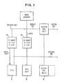
- FIG. 1 an overall organizational block diagram of a typical PRISM system architecture is shown.
- the CPU 12 is depicted as a separate unit, however, it will be understood that the internal bus 10 is actually a composite member of the basic CPU architecture.
- Specific units shown directly attached to the internal bus 10 are the floating point unit 14 and a block designated other bus units 16 which, as will be readily understood, may comprise a plurality of different units separately attached to the bus 10.
- the instruction cache 18 and data cache 20 are also illustrated as connected to the internal bus and thus operable under various internal bus operation instruction formats (described previously).
- a system bus unit 22 is also shown connected to the internal bus which would primarily perform the function of system I/O operations to and from main storage as will be understood by those skilled in the art. No specific instructions for controlling the system bus unit are described herein, however, operation instruction to control such a system bus unit are well known and would be obvious to skilled in the art.
- FIGS. 2A and 2B form a composite functional block and data flow diagram for the PRISM CPU. These two figures are organized as shown in the organizational diagram of FIG. 2.
- FIGS. 2A and 2B The data flow within the basic PRISM organization is clearly shown in FIGS. 2A and 2B.
- the basic CPU includes a five ports general purpose registers block 30 containing thirty two individual registers.
- the two inputs to the register block RT and RA as well as the three outputs RA, RB, RS indicate the particular instruction designated operands set forth in the previous description of the instruction formats.
- the (address of the) particular general purpose register in which the various operands are to be stored or from which they are to be fetched would be specified in the various fields of the instruction register.
- the organization of the instruction register 32 is straightforward. It should be noted that this is a 32-bit register with the various delineated fields within the register clearly shown in the drawing (designated bits) as well as the mnemonic representations of the various fields as used in the previously described instruction formats.
- the designated BI, SH and M beneath the primary instruction register box 32 indicates the mnemonic representation given to these fields in certain of the instructions. However, it should be understood that these are shown outside of the instruction box for convenience of reference only.
- the instruction address register (IAR) 34 is also conventional in nature and would be initially loaded at the beginning of a program and suitably incremented or reloaded by the program subsequently as required.
- Block 36 labeled (IAR +4) contains the next instruction address.
- the two multiplexers 38 and 40 may receive as input operands various fields from the instruction address register 34, instruction register 32 and the specified operands RA, RB from the general purpose registers 30.
- the ALU 42 performs two operand operations and places the result in output buffer register 44.
- the output from the ALU may also go directly to the instruction address register 34, the condition logic and condition register block 50, the branch and trap testing logic 52 and the address gate 54 which supplies addresses to the system memory when required.
- the output of the buffer register 44 is able to return data to the general purpose registers 30 via the multiplexers 46 and 48 depending upon whether the field RA or RT is specified by the instruction.
- the mask and rotate logic block 56 performs a one-machine cycle executable mask and rotate operation set forth in more detail in copending application serial no. 509836 (Y0983-011) referenced previously and does not enter directly into the present "branch" instructions. Similarily, the details of the condition logic and condition register block 50 are the subject matter of previously referenced copending application serial no. 509744 (Y0983-009).
- Block 52 entitled branch and trap testing comprises the circuitry necessary to perform the trap testing function and produce a trap interrupt if necessary and also to perform present "branch-on-any-bit-in-any-register" testing of the present invention.
- Gates 55 and 58 serve to gate data to and from the system memory as required for certain specified operations. Gates 54, 55 and 58 together with the 'Address' and 'Data' Buses comprise the Data Cache Interface.
- the register MQ shown in the mask and rotate logic block 56 is an extension register for storing the overflow contents from a number of arithmetic operations such as multiply and divide. It is functionally located in this block for purposes of the present embodiment as it is utilized during certain mask and rotate instructions which are set forth and claimed in copending application serial no. 509836 (YO983-0ll).
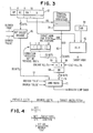
- FIG. 3 comprises a combination functional block and a flow diagram of the CPU similar to FIG. 2. It pertains strictly to that portion of the CPU which is active during execution of the present branch-on-any-bit-in-any-register instructions.
- the same reference numerals are used as in FIG. 2 for the same functional blocks. It will be noted that the additional hardware necessitated by the present mechanism is shown essentially at the bottom of the figure.
- condition register architecture For a more detailed description of the specific condition register architecture, reference may be made to the previously set forth concurrently filed application serial no. 509744 (IBM Y0983-009). However, it is to be clearly understood that the particular condition which caused a bit to be set in one of these registers is not relevant to the present invention where the bit is stored (i.e., what register) in the system and subsequently accessed for branch testing purposes is, of course, relevant. Thus the present invention could be utilized in a more conventional CPU configuration having a much smaller condition register than that described in the above copending application.
- the BI field from the instruction register 32 feeds into the bit select decoder 60.
- this is a 5-bit field and the bits selected the decoder, produces 32-bit output which will have the fields of zeros with a 1-bit pointed to by the BI fields set 1, if a branch true conditions is to be tested for. Alternatively, if a branch false condition is to be tested for the output of the decoder 60 will be a field of ones with a zero in the bit position specified by the BI field.
- the RA field in the instruction register utilized address one of the 32 general purpose registers pointed to by the particular address present in the RA field. If the address RA is not all zeros one of the GPR registers will be selected and its output placed on line 62.
- the 32-bit bus is connected to AND gate 64. It will be noted that AND gate 66 is connected to the 32-bit output from the condition register.
- the address RA is set to all zeros specified that the condition register is directed to be tested. If it is set to any other number it indicates that one of the GPR registers is to be tested.
- Two lines forming the other input to the AND gates 64 and 66 are connected to circuitry (not shown) which tests the condition of the R A field. If the RA field is not all zeros as indicated in register 64, it will become active and the contents of register RA will pass through OR circuit 68 into the AND mask 70. Conversely, if field RA were set at all zeros and the condition register must be accessed AND gate 66 becomes active and the contents of the condition register will pass through OR gate 68 into the AND mask circuit 70 where the actual branch is performed.
- the operation of the AND mask 70 is quite straightforward and is in this case called an AND mask since in effect, the 32-bit field from decoder 60 which is placed on cable 72 operates as a mask since, if a 'branch true' condition occurs, it will be set to all zeros with a 1 in the bit position to be tested. Thus an output will be produced from the circuit only if a one similarly exists in the same bit position in the register being tested which enters AND mask 70 via cable 74. Similarly for the branch false condition the mask entering over cable 72 would be a field of all l's with exception of the '0' in the particular bit to be tested. This way output will be produced from block 70 only if the '0' occurs in the designated bit position in the register to be tested entering via cable 74.
- the logic function performed by block 70 would be a straightforward AND function in each bit position flowing into a 32 input OR circuit.
- BA NAND function both inputs must be zero
- BA NAND function both inputs must be zero
- a specific embodiment for the AND mask 70 could comprise the cables 72 and 74 feeding in parallel into conventional 32 bit AND circuit and 32 bit NAND circuit with the outputs going to the appropriate switching gates into the aforementioned 32 bit OR circuit.
- Neither the AND nor the NAND circuit outputs utilizes the input to the OR circuit could be determined by the branch true and branch false lines shown. There are doubtless many other embodiments we could perform with the same logical functions. One shown is considered to be the simplest and most straightforward.
- FIG. 4 is essentially a timing chart of the operations which occur during the execution of the herein disclosed one machine cycle executable branch-on-any-bit in any register instructions.
- the event entitled READ/WRITE GPR refers to the reading and writing (previous instruction) of the registers of the GPRs specified by the fields at the instructions specifying GPR addresses, e.g., the RA field and the RB field in the case of an X-form branch instruction as described previously.
- the contents (RB) from the register pointed to by the RB field would comprise the target address for the next instruction for an X-form instruction.
- target address computes the target address whether X-form or D-form in parallel with branch testing so that at the end of the branch instruction cycle the system is computed, the branch or jump target address, whether or not it is needed. If it is needed it is available to the beginning of the next instruction and if not needed it is of course ignored. In this way, substantially all of the functions required of the system in such a branch test operation are completed in one machine cycle. This will be apparent to those skilled in the art. An additional cycle would be required for the target instruction fetch utilizing the target instruction address computed during the branch instruction cycle.
- the compiler might have inserted a "with execute” branch instruction in the instruction stream whereby an additional instruction could be executed in parallel with the target instruction fetch.
Applications Claiming Priority (2)
| Application Number | Priority Date | Filing Date | Title |
|---|---|---|---|
| US50973483A | 1983-06-30 | 1983-06-30 | |
| US509734 | 1983-06-30 |
Publications (2)
| Publication Number | Publication Date |
|---|---|
| EP0130381A2 true EP0130381A2 (fr) | 1985-01-09 |
| EP0130381A3 EP0130381A3 (fr) | 1987-11-19 |
Family
ID=24027883
Family Applications (1)
| Application Number | Title | Priority Date | Filing Date |
|---|---|---|---|
| EP84106179A Withdrawn EP0130381A3 (fr) | 1983-06-30 | 1984-05-30 | Mécanisme pour la réalisation d'instructions d'aiguillage sur n'importe quel bit dans n'importe quel registre exécutable en un cycle de machine dans un système ordinateur à jeu d'instructions primitif |
Country Status (2)
| Country | Link |
|---|---|
| EP (1) | EP0130381A3 (fr) |
| JP (1) | JPS6014338A (fr) |
Cited By (12)
| Publication number | Priority date | Publication date | Assignee | Title |
|---|---|---|---|---|
| EP0297890A2 (fr) * | 1987-07-01 | 1989-01-04 | Digital Equipment Corporation | Dispositif et procédé de signalisation de condition induite par des données |
| EP0301708A2 (fr) * | 1987-07-02 | 1989-02-01 | General Datacomm, Inc. | Unité arithmétique logique parallèle |
| EP0363174A2 (fr) * | 1988-10-07 | 1990-04-11 | International Business Machines Corporation | Traitement de branchement sur bit |
| US5278840A (en) * | 1987-07-01 | 1994-01-11 | Digital Equipment Corporation | Apparatus and method for data induced condition signalling |
| EP1236097A1 (fr) * | 1999-09-01 | 2002-09-04 | Intel Corporation | Instruction de branchement pour processeur |
| EP1267255A2 (fr) * | 2001-06-11 | 2002-12-18 | Broadcom Corporation | Exécution de branchement conditionnel dans un processeur à chemins de données multiples |
| US7127593B2 (en) | 2001-06-11 | 2006-10-24 | Broadcom Corporation | Conditional execution with multiple destination stores |
| US7287152B2 (en) | 2001-06-11 | 2007-10-23 | Broadcom Corporation | Conditional execution per lane |
| US7299343B2 (en) * | 2002-09-27 | 2007-11-20 | Verisilicon Holdings (Cayman Islands) Co. Ltd. | System and method for cooperative execution of multiple branching instructions in a processor |
| US7434036B1 (en) * | 2002-08-30 | 2008-10-07 | Verisilicon Holdings Co. Ltd. | System and method for executing software program instructions using a condition specified within a conditional execution instruction |
| US7681018B2 (en) | 2000-08-31 | 2010-03-16 | Intel Corporation | Method and apparatus for providing large register address space while maximizing cycletime performance for a multi-threaded register file set |
| US7991983B2 (en) | 1999-09-01 | 2011-08-02 | Intel Corporation | Register set used in multithreaded parallel processor architecture |
Families Citing this family (2)
| Publication number | Priority date | Publication date | Assignee | Title |
|---|---|---|---|---|
| US7302555B2 (en) * | 2003-04-29 | 2007-11-27 | Koninklijke Philips Electronics, N.V. | Zero overhead branching and looping in time stationary processors |
| US7958181B2 (en) * | 2006-09-21 | 2011-06-07 | Intel Corporation | Method and apparatus for performing logical compare operations |
Citations (1)
| Publication number | Priority date | Publication date | Assignee | Title |
|---|---|---|---|---|
| US4334268A (en) * | 1979-05-01 | 1982-06-08 | Motorola, Inc. | Microcomputer with branch on bit set/clear instructions |
Family Cites Families (3)
| Publication number | Priority date | Publication date | Assignee | Title |
|---|---|---|---|---|
| DE2331747A1 (de) * | 1973-06-22 | 1975-01-30 | Benteler Werke Ag | Vorrichtung und verfahren zum kontinuierlichen verschweissen eines geschlitzten rohrstranges |
| JPS5588140A (en) * | 1978-12-27 | 1980-07-03 | Hitachi Ltd | Address branch system of microprogram controller |
| JPS5837746A (ja) * | 1981-08-31 | 1983-03-05 | Nippon Telegr & Teleph Corp <Ntt> | 条件判定処理装置 |
-
1984
- 1984-04-20 JP JP59078784A patent/JPS6014338A/ja active Pending
- 1984-05-30 EP EP84106179A patent/EP0130381A3/fr not_active Withdrawn
Patent Citations (1)
| Publication number | Priority date | Publication date | Assignee | Title |
|---|---|---|---|---|
| US4334268A (en) * | 1979-05-01 | 1982-06-08 | Motorola, Inc. | Microcomputer with branch on bit set/clear instructions |
Non-Patent Citations (3)
| Title |
|---|
| IBM TECHNICAL DISCLOSURE BULLETIN, vol. 19, no. 11, April 1977, pages 4369-4370, New York, US; R.C. BOOTH et al.: "Save/restore ALU condition register" * |
| IBM TECHNICAL DISCLOSURE BULLETIN, vol. 24, no. 6, November 1981, page 2698, New York, US; T.A: GREGG et al.: "Jump on bit instruction" * |
| IEEE COMPUTER SOCIETY INTERNATIONAL CONFERENCE, DIGEST OF PAPERS, 28th February - 3rd March 1983, Los Angeles, pages 278-285, IEEE, New York, US; T.R. GROSS: "Code optimization techniques for pipelines architectures" * |
Cited By (21)
| Publication number | Priority date | Publication date | Assignee | Title |
|---|---|---|---|---|
| AU626264B2 (en) * | 1987-07-01 | 1992-07-30 | Digital Equipment Corporation | Apparatus and method for data induced condition signaling |
| EP0297890A3 (fr) * | 1987-07-01 | 1990-07-11 | Digital Equipment Corporation | Dispositif et procédé de signalisation de condition induite par des données |
| US5278840A (en) * | 1987-07-01 | 1994-01-11 | Digital Equipment Corporation | Apparatus and method for data induced condition signalling |
| EP0297890A2 (fr) * | 1987-07-01 | 1989-01-04 | Digital Equipment Corporation | Dispositif et procédé de signalisation de condition induite par des données |
| EP0301708A2 (fr) * | 1987-07-02 | 1989-02-01 | General Datacomm, Inc. | Unité arithmétique logique parallèle |
| EP0301708A3 (fr) * | 1987-07-02 | 1991-03-20 | General Datacomm, Inc. | Unité arithmétique logique parallèle |
| EP0363174A2 (fr) * | 1988-10-07 | 1990-04-11 | International Business Machines Corporation | Traitement de branchement sur bit |
| EP0363174A3 (fr) * | 1988-10-07 | 1992-07-08 | International Business Machines Corporation | Traitement de branchement sur bit |
| EP1236097A1 (fr) * | 1999-09-01 | 2002-09-04 | Intel Corporation | Instruction de branchement pour processeur |
| US7991983B2 (en) | 1999-09-01 | 2011-08-02 | Intel Corporation | Register set used in multithreaded parallel processor architecture |
| EP1236097A4 (fr) * | 1999-09-01 | 2006-08-02 | Intel Corp | Instruction de branchement pour processeur |
| US7681018B2 (en) | 2000-08-31 | 2010-03-16 | Intel Corporation | Method and apparatus for providing large register address space while maximizing cycletime performance for a multi-threaded register file set |
| US7743235B2 (en) | 2000-08-31 | 2010-06-22 | Intel Corporation | Processor having a dedicated hash unit integrated within |
| EP1267255A3 (fr) * | 2001-06-11 | 2003-05-02 | Broadcom Corporation | Exécution de branchement conditionnel dans un processeur à chemins de données multiples |
| US7287152B2 (en) | 2001-06-11 | 2007-10-23 | Broadcom Corporation | Conditional execution per lane |
| US7127593B2 (en) | 2001-06-11 | 2006-10-24 | Broadcom Corporation | Conditional execution with multiple destination stores |
| US7861071B2 (en) | 2001-06-11 | 2010-12-28 | Broadcom Corporation | Conditional branch instruction capable of testing a plurality of indicators in a predicate register |
| EP1267255A2 (fr) * | 2001-06-11 | 2002-12-18 | Broadcom Corporation | Exécution de branchement conditionnel dans un processeur à chemins de données multiples |
| US8521997B2 (en) | 2001-06-11 | 2013-08-27 | Broadcom Corporation | Conditional execution with multiple destination stores |
| US7434036B1 (en) * | 2002-08-30 | 2008-10-07 | Verisilicon Holdings Co. Ltd. | System and method for executing software program instructions using a condition specified within a conditional execution instruction |
| US7299343B2 (en) * | 2002-09-27 | 2007-11-20 | Verisilicon Holdings (Cayman Islands) Co. Ltd. | System and method for cooperative execution of multiple branching instructions in a processor |
Also Published As
| Publication number | Publication date |
|---|---|
| EP0130381A3 (fr) | 1987-11-19 |
| JPS6014338A (ja) | 1985-01-24 |
Similar Documents
| Publication | Publication Date | Title |
|---|---|---|
| US4569016A (en) | Mechanism for implementing one machine cycle executable mask and rotate instructions in a primitive instruction set computing system | |
| US4589065A (en) | Mechanism for implementing one machine cycle executable trap instructions in a primitive instruction set computing system | |
| EP0130377B1 (fr) | Architecture de registre de condition pour machine à jeu d'instructions primitif | |
| US4399507A (en) | Instruction address stack in the data memory of an instruction-pipelined processor | |
| US4740893A (en) | Method for reducing the time for switching between programs | |
| KR0160602B1 (ko) | 데이터 처리장치 | |
| US5375216A (en) | Apparatus and method for optimizing performance of a cache memory in a data processing system | |
| US4777594A (en) | Data processing apparatus and method employing instruction flow prediction | |
| EP0352103B1 (fr) | Ecrasement des bulles du pipeline dans un système de calcul | |
| KR100190252B1 (ko) | 고속 프로세서에서의 브랜치 처리 방법 및 장치 | |
| US4947316A (en) | Internal bus architecture employing a simplified rapidly executable instruction set | |
| US5729724A (en) | Adaptive 128-bit floating point load and store operations for quadruple precision compatibility | |
| US20010010072A1 (en) | Instruction translator translating non-native instructions for a processor into native instructions therefor, instruction memory with such translator, and data processing apparatus using them | |
| EP0405495B1 (fr) | Dispositif logique et méthode de gestion d'une unité d'instruction dans une unité de traitement en pipeline | |
| US5905881A (en) | Delayed state writes for an instruction processor | |
| EP0130381A2 (fr) | Mécanisme pour la réalisation d'instructions d'aiguillage sur n'importe quel bit dans n'importe quel registre exécutable en un cycle de machine dans un système ordinateur à jeu d'instructions primitif | |
| US4562538A (en) | Microprocessor having decision pointer to process restore position | |
| JPS6339931B2 (fr) | ||
| US5097407A (en) | Artificial intelligence processor | |
| EP0772819B1 (fr) | Appareil et procede pour determiner avec efficacite des adresses pour les donnees presentant une erreur d'alignement en memoire | |
| KR100303712B1 (ko) | 파이프라인기계에서의어드레스파이프라인을위한방법및장치 | |
| US5333287A (en) | System for executing microinstruction routines by using hardware to calculate initialization parameters required therefore based upon processor status and control parameters | |
| US5666507A (en) | Pipelined microinstruction apparatus and methods with branch prediction and speculative state changing | |
| US5590293A (en) | Dynamic microbranching with programmable hold on condition, to programmable dynamic microbranching delay minimization | |
| US5363490A (en) | Apparatus for and method of conditionally aborting an instruction within a pipelined architecture |
Legal Events
| Date | Code | Title | Description |
|---|---|---|---|
| PUAI | Public reference made under article 153(3) epc to a published international application that has entered the european phase |
Free format text: ORIGINAL CODE: 0009012 |
|
| AK | Designated contracting states |
Designated state(s): DE FR GB |
|
| 17P | Request for examination filed |
Effective date: 19841123 |
|
| PUAL | Search report despatched |
Free format text: ORIGINAL CODE: 0009013 |
|
| AK | Designated contracting states |
Kind code of ref document: A3 Designated state(s): DE FR GB |
|
| 17Q | First examination report despatched |
Effective date: 19890403 |
|
| STAA | Information on the status of an ep patent application or granted ep patent |
Free format text: STATUS: THE APPLICATION IS DEEMED TO BE WITHDRAWN |
|
| 18D | Application deemed to be withdrawn |
Effective date: 19891014 |
|
| RIN1 | Information on inventor provided before grant (corrected) |
Inventor name: RADIN, GEORGE Inventor name: WORLEY, WILLIAM SPENCER, JR. Inventor name: AUSLANDER, MARC ALAN Inventor name: MARKSTEIN, PETER WILLY Inventor name: HAO, HSIEH TUNG Inventor name: HOPKINS, MARTIN EDWARD |