EP0023988B1 - Verwendung eines leitenden organischen Ladungsübertragungsmaterials als elektronenstrahlempfindliches Resistmaterial und Verfahren zur Herstellung positiver und negativer Resistbilder - Google Patents
Verwendung eines leitenden organischen Ladungsübertragungsmaterials als elektronenstrahlempfindliches Resistmaterial und Verfahren zur Herstellung positiver und negativer Resistbilder Download PDFInfo
- Publication number
- EP0023988B1 EP0023988B1 EP80104214A EP80104214A EP0023988B1 EP 0023988 B1 EP0023988 B1 EP 0023988B1 EP 80104214 A EP80104214 A EP 80104214A EP 80104214 A EP80104214 A EP 80104214A EP 0023988 B1 EP0023988 B1 EP 0023988B1
- Authority
- EP
- European Patent Office
- Prior art keywords
- iodines
- chlorines
- bromines
- accordance
- film
- Prior art date
- Legal status (The legal status is an assumption and is not a legal conclusion. Google has not performed a legal analysis and makes no representation as to the accuracy of the status listed.)
- Expired
Links
- 239000000463 material Substances 0.000 title claims description 40
- 238000010894 electron beam technology Methods 0.000 title claims description 22
- 238000012546 transfer Methods 0.000 title claims description 18
- 238000000034 method Methods 0.000 title claims description 11
- 229920002120 photoresistant polymer Polymers 0.000 title claims description 8
- 239000000203 mixture Substances 0.000 title description 5
- ZCYVEMRRCGMTRW-UHFFFAOYSA-N 7553-56-2 Chemical class [I] ZCYVEMRRCGMTRW-UHFFFAOYSA-N 0.000 claims description 12
- 150000003839 salts Chemical class 0.000 claims description 12
- 239000002904 solvent Substances 0.000 claims description 9
- 238000004519 manufacturing process Methods 0.000 claims description 8
- CJVYYDCBKKKIPD-UHFFFAOYSA-N 1-n,1-n,2-n,2-n-tetramethylbenzene-1,2-diamine Chemical compound CN(C)C1=CC=CC=C1N(C)C CJVYYDCBKKKIPD-UHFFFAOYSA-N 0.000 claims description 6
- CSHWQDPOILHKBI-UHFFFAOYSA-N peryrene Natural products C1=CC(C2=CC=CC=3C2=C2C=CC=3)=C3C2=CC=CC3=C1 CSHWQDPOILHKBI-UHFFFAOYSA-N 0.000 claims description 6
- 125000000217 alkyl group Chemical group 0.000 claims description 5
- 125000004836 hexamethylene group Chemical group [H]C([H])([*:2])C([H])([H])C([H])([H])C([H])([H])C([H])([H])C([H])([H])[*:1] 0.000 claims description 5
- 125000002080 perylenyl group Chemical group C1(=CC=C2C=CC=C3C4=CC=CC5=CC=CC(C1=C23)=C45)* 0.000 claims description 4
- IEQIEDJGQAUEQZ-UHFFFAOYSA-N phthalocyanine Chemical compound N1C(N=C2C3=CC=CC=C3C(N=C3C4=CC=CC=C4C(=N4)N3)=N2)=C(C=CC=C2)C2=C1N=C1C2=CC=CC=C2C4=N1 IEQIEDJGQAUEQZ-UHFFFAOYSA-N 0.000 claims description 4
- 239000000758 substrate Substances 0.000 claims description 4
- FSBQGCIXVCZLAE-UHFFFAOYSA-N CN1C(C(C)=C2C3=CC=CC=C3C(C(C)=C3C4=CC=CC=C4C(=C4C)N3C)=N2)=C(C=CC=C2)C2=C1C(C)=C1C2=C(C)C(C)=CC=C2C4=N1 Chemical compound CN1C(C(C)=C2C3=CC=CC=C3C(C(C)=C3C4=CC=CC=C4C(=C4C)N3C)=N2)=C(C=CC=C2)C2=C1C(C)=C1C2=C(C)C(C)=CC=C2C4=N1 FSBQGCIXVCZLAE-UHFFFAOYSA-N 0.000 claims description 3
- 125000001997 phenyl group Chemical group [H]C1=C([H])C([H])=C(*)C([H])=C1[H] 0.000 claims description 3
- KMHSUNDEGHRBNV-UHFFFAOYSA-N 2,4-dichloropyrimidine-5-carbonitrile Chemical compound ClC1=NC=C(C#N)C(Cl)=N1 KMHSUNDEGHRBNV-UHFFFAOYSA-N 0.000 claims description 2
- 238000004132 cross linking Methods 0.000 claims description 2
- 125000001246 bromo group Chemical class Br* 0.000 claims 11
- 235000017168 chlorine Nutrition 0.000 claims 11
- 125000001309 chloro group Chemical class Cl* 0.000 claims 11
- 235000013675 iodine Nutrition 0.000 claims 11
- UFPVYWYEZPMUQL-UHFFFAOYSA-N 2-(1,3-diselenol-2-ylidene)-1,3-diselenole Chemical compound [Se]1C=C[Se]C1=C1[Se]C=C[Se]1 UFPVYWYEZPMUQL-UHFFFAOYSA-N 0.000 claims 1
- BTQDPOVTMFCMKB-UHFFFAOYSA-N 2-(1,3-dithiol-2-ylidene)-4,5-dimethyl-1,3-dithiole Chemical compound S1C(C)=C(C)SC1=C1SC=CS1 BTQDPOVTMFCMKB-UHFFFAOYSA-N 0.000 claims 1
- YMWLPMGFZYFLRP-UHFFFAOYSA-N 2-(4,5-dimethyl-1,3-diselenol-2-ylidene)-4,5-dimethyl-1,3-diselenole Chemical compound [Se]1C(C)=C(C)[Se]C1=C1[Se]C(C)=C(C)[Se]1 YMWLPMGFZYFLRP-UHFFFAOYSA-N 0.000 claims 1
- HGOTVGUTJPNVDR-UHFFFAOYSA-N 2-(4,5-dimethyl-1,3-dithiol-2-ylidene)-4,5-dimethyl-1,3-dithiole Chemical compound S1C(C)=C(C)SC1=C1SC(C)=C(C)S1 HGOTVGUTJPNVDR-UHFFFAOYSA-N 0.000 claims 1
- VRSXBMGXAHSMFB-UHFFFAOYSA-N 2-(5,6-dihydro-4h-cyclopenta[d][1,3]diselenol-2-ylidene)-5,6-dihydro-4h-cyclopenta[d][1,3]diselenole Chemical compound C1CCC([Se]2)=C1[Se]C2=C([Se]1)[Se]C2=C1CCC2 VRSXBMGXAHSMFB-UHFFFAOYSA-N 0.000 claims 1
- DTJPUCUJANTIIU-UHFFFAOYSA-N 2-(5,6-dihydro-4h-cyclopenta[d][1,3]dithiol-2-ylidene)-5,6-dihydro-4h-cyclopenta[d][1,3]dithiole Chemical compound C1CCC(S2)=C1SC2=C(S1)SC2=C1CCC2 DTJPUCUJANTIIU-UHFFFAOYSA-N 0.000 claims 1
- DXMJKBPWGFMCAW-UHFFFAOYSA-N 3,4,5,6-tetramethyldithiine Chemical compound CC1=C(C)C(C)=C(C)SS1 DXMJKBPWGFMCAW-UHFFFAOYSA-N 0.000 claims 1
- GQKHQLQFHZVMAF-UHFFFAOYSA-N 3,4,5,6-tetraphenyldithiine Chemical compound S1SC(C=2C=CC=CC=2)=C(C=2C=CC=CC=2)C(C=2C=CC=CC=2)=C1C1=CC=CC=C1 GQKHQLQFHZVMAF-UHFFFAOYSA-N 0.000 claims 1
- WDEQGLDWZMIMJM-UHFFFAOYSA-N benzyl 4-hydroxy-2-(hydroxymethyl)pyrrolidine-1-carboxylate Chemical compound OCC1CC(O)CN1C(=O)OCC1=CC=CC=C1 WDEQGLDWZMIMJM-UHFFFAOYSA-N 0.000 claims 1
- MPMSMUBQXQALQI-UHFFFAOYSA-N cobalt phthalocyanine Chemical compound [Co+2].C12=CC=CC=C2C(N=C2[N-]C(C3=CC=CC=C32)=N2)=NC1=NC([C]1C=CC=CC1=1)=NC=1N=C1[C]3C=CC=CC3=C2[N-]1 MPMSMUBQXQALQI-UHFFFAOYSA-N 0.000 claims 1
- RBTKNAXYKSUFRK-UHFFFAOYSA-N heliogen blue Chemical compound [Cu].[N-]1C2=C(C=CC=C3)C3=C1N=C([N-]1)C3=CC=CC=C3C1=NC([N-]1)=C(C=CC=C3)C3=C1N=C([N-]1)C3=CC=CC=C3C1=N2 RBTKNAXYKSUFRK-UHFFFAOYSA-N 0.000 claims 1
- FHCPAXDKURNIOZ-UHFFFAOYSA-N tetrathiafulvalene Chemical compound S1C=CSC1=C1SC=CS1 FHCPAXDKURNIOZ-UHFFFAOYSA-N 0.000 claims 1
- 230000003287 optical effect Effects 0.000 description 15
- 229910052736 halogen Inorganic materials 0.000 description 9
- 150000002367 halogens Chemical class 0.000 description 8
- PXHVJJICTQNCMI-UHFFFAOYSA-N Nickel Chemical compound [Ni] PXHVJJICTQNCMI-UHFFFAOYSA-N 0.000 description 7
- 238000010521 absorption reaction Methods 0.000 description 7
- 238000011161 development Methods 0.000 description 7
- CPELXLSAUQHCOX-UHFFFAOYSA-M Bromide Chemical compound [Br-] CPELXLSAUQHCOX-UHFFFAOYSA-M 0.000 description 6
- IAZDPXIOMUYVGZ-UHFFFAOYSA-N Dimethylsulphoxide Chemical compound CS(C)=O IAZDPXIOMUYVGZ-UHFFFAOYSA-N 0.000 description 6
- 230000009102 absorption Effects 0.000 description 6
- OAKJQQAXSVQMHS-UHFFFAOYSA-N Hydrazine Chemical compound NN OAKJQQAXSVQMHS-UHFFFAOYSA-N 0.000 description 4
- 230000008901 benefit Effects 0.000 description 4
- MVPPADPHJFYWMZ-UHFFFAOYSA-N chlorobenzene Chemical compound ClC1=CC=CC=C1 MVPPADPHJFYWMZ-UHFFFAOYSA-N 0.000 description 4
- 238000000576 coating method Methods 0.000 description 4
- 230000005855 radiation Effects 0.000 description 4
- 230000035945 sensitivity Effects 0.000 description 4
- 230000003068 static effect Effects 0.000 description 4
- 238000000859 sublimation Methods 0.000 description 4
- 230000008022 sublimation Effects 0.000 description 4
- 229910052723 transition metal Inorganic materials 0.000 description 4
- LXULCFYNNJMINH-UHFFFAOYSA-N 3,4,5,6-tetraphenyl-2-(2h-pyran-2-yldisulfanyl)-2h-pyran Chemical compound O1C=CC=CC1SSC1C(C=2C=CC=CC=2)=C(C=2C=CC=CC=2)C(C=2C=CC=CC=2)=C(C=2C=CC=CC=2)O1 LXULCFYNNJMINH-UHFFFAOYSA-N 0.000 description 3
- WEVYAHXRMPXWCK-UHFFFAOYSA-N Acetonitrile Chemical compound CC#N WEVYAHXRMPXWCK-UHFFFAOYSA-N 0.000 description 3
- YMWUJEATGCHHMB-UHFFFAOYSA-N Dichloromethane Chemical compound ClCCl YMWUJEATGCHHMB-UHFFFAOYSA-N 0.000 description 3
- OKKJLVBELUTLKV-UHFFFAOYSA-N Methanol Chemical compound OC OKKJLVBELUTLKV-UHFFFAOYSA-N 0.000 description 3
- ZMXDDKWLCZADIW-UHFFFAOYSA-N N,N-Dimethylformamide Chemical compound CN(C)C=O ZMXDDKWLCZADIW-UHFFFAOYSA-N 0.000 description 3
- 239000011248 coating agent Substances 0.000 description 3
- GUTLYIVDDKVIGB-UHFFFAOYSA-N cobalt atom Chemical compound [Co] GUTLYIVDDKVIGB-UHFFFAOYSA-N 0.000 description 3
- 238000005516 engineering process Methods 0.000 description 3
- 238000005259 measurement Methods 0.000 description 3
- 229910052759 nickel Inorganic materials 0.000 description 3
- BASFCYQUMIYNBI-UHFFFAOYSA-N platinum Chemical compound [Pt] BASFCYQUMIYNBI-UHFFFAOYSA-N 0.000 description 3
- 229920000642 polymer Polymers 0.000 description 3
- 230000008569 process Effects 0.000 description 3
- 238000003860 storage Methods 0.000 description 3
- WVKLPDQDLBOBGZ-UHFFFAOYSA-N 3,4,5,6-tetramethyl-2-(2h-pyran-2-yldiselanyl)-2h-pyran Chemical compound O1C(C)=C(C)C(C)=C(C)C1[Se][Se]C1C=CC=CO1 WVKLPDQDLBOBGZ-UHFFFAOYSA-N 0.000 description 2
- IJOPJHSZEGWWAM-UHFFFAOYSA-N 3,4,5,6-tetramethyl-2-(2h-pyran-2-yldisulfanyl)-2h-pyran Chemical compound O1C(C)=C(C)C(C)=C(C)C1SSC1C=CC=CO1 IJOPJHSZEGWWAM-UHFFFAOYSA-N 0.000 description 2
- JTDAMRMAUUQNBG-UHFFFAOYSA-N 3,4,5,6-tetraphenyl-2-(2h-pyran-2-yldiselanyl)-2h-pyran Chemical compound O1C=CC=CC1[Se][Se]C1C(C=2C=CC=CC=2)=C(C=2C=CC=CC=2)C(C=2C=CC=CC=2)=C(C=2C=CC=CC=2)O1 JTDAMRMAUUQNBG-UHFFFAOYSA-N 0.000 description 2
- WKBOTKDWSSQWDR-UHFFFAOYSA-N Bromine atom Chemical compound [Br] WKBOTKDWSSQWDR-UHFFFAOYSA-N 0.000 description 2
- ZAMOUSCENKQFHK-UHFFFAOYSA-N Chlorine atom Chemical compound [Cl] ZAMOUSCENKQFHK-UHFFFAOYSA-N 0.000 description 2
- HEDRZPFGACZZDS-UHFFFAOYSA-N Chloroform Chemical compound ClC(Cl)Cl HEDRZPFGACZZDS-UHFFFAOYSA-N 0.000 description 2
- RYGMFSIKBFXOCR-UHFFFAOYSA-N Copper Chemical compound [Cu] RYGMFSIKBFXOCR-UHFFFAOYSA-N 0.000 description 2
- XEEYBQQBJWHFJM-UHFFFAOYSA-N Iron Chemical compound [Fe] XEEYBQQBJWHFJM-UHFFFAOYSA-N 0.000 description 2
- JKPYOWXCHRIGII-UHFFFAOYSA-N [Ni].CN1C(C(C)=C2C3=CC=CC=C3C(C(C)=C3C4=CC=CC=C4C(=C4C)N3C)=N2)=C(C=CC=C2)C2=C1C(C)=C1C2=C(C)C(C)=CC=C2C4=N1 Chemical compound [Ni].CN1C(C(C)=C2C3=CC=CC=C3C(C(C)=C3C4=CC=CC=C4C(=C4C)N3C)=N2)=C(C=CC=C2)C2=C1C(C)=C1C2=C(C)C(C)=CC=C2C4=N1 JKPYOWXCHRIGII-UHFFFAOYSA-N 0.000 description 2
- 238000004458 analytical method Methods 0.000 description 2
- 238000009835 boiling Methods 0.000 description 2
- GDTBXPJZTBHREO-UHFFFAOYSA-N bromine Substances BrBr GDTBXPJZTBHREO-UHFFFAOYSA-N 0.000 description 2
- 229910052794 bromium Inorganic materials 0.000 description 2
- 150000001649 bromium compounds Chemical class 0.000 description 2
- 230000008859 change Effects 0.000 description 2
- 238000006243 chemical reaction Methods 0.000 description 2
- 229910052801 chlorine Inorganic materials 0.000 description 2
- 239000000460 chlorine Substances 0.000 description 2
- 229910017052 cobalt Inorganic materials 0.000 description 2
- 239000010941 cobalt Substances 0.000 description 2
- 229910052802 copper Inorganic materials 0.000 description 2
- 239000010949 copper Substances 0.000 description 2
- 238000011065 in-situ storage Methods 0.000 description 2
- 230000010354 integration Effects 0.000 description 2
- 150000004694 iodide salts Chemical class 0.000 description 2
- 150000002500 ions Chemical class 0.000 description 2
- 125000002496 methyl group Chemical group [H]C([H])([H])* 0.000 description 2
- 230000007935 neutral effect Effects 0.000 description 2
- 238000000206 photolithography Methods 0.000 description 2
- 239000002798 polar solvent Substances 0.000 description 2
- 150000004032 porphyrins Chemical class 0.000 description 2
- 239000000126 substance Substances 0.000 description 2
- VZGDMQKNWNREIO-UHFFFAOYSA-N tetrachloromethane Chemical compound ClC(Cl)(Cl)Cl VZGDMQKNWNREIO-UHFFFAOYSA-N 0.000 description 2
- 238000006276 transfer reaction Methods 0.000 description 2
- 150000003624 transition metals Chemical class 0.000 description 2
- VEXZGXHMUGYJMC-UHFFFAOYSA-M Chloride anion Chemical compound [Cl-] VEXZGXHMUGYJMC-UHFFFAOYSA-M 0.000 description 1
- -1 Halogen salts Chemical class 0.000 description 1
- 230000009471 action Effects 0.000 description 1
- 150000001298 alcohols Chemical class 0.000 description 1
- 239000003795 chemical substances by application Substances 0.000 description 1
- 150000001805 chlorine compounds Chemical class 0.000 description 1
- 239000008139 complexing agent Substances 0.000 description 1
- 150000001875 compounds Chemical class 0.000 description 1
- 229920001577 copolymer Polymers 0.000 description 1
- 238000000151 deposition Methods 0.000 description 1
- 238000000609 electron-beam lithography Methods 0.000 description 1
- 230000008030 elimination Effects 0.000 description 1
- 238000003379 elimination reaction Methods 0.000 description 1
- 238000010438 heat treatment Methods 0.000 description 1
- XMBWDFGMSWQBCA-UHFFFAOYSA-N hydrogen iodide Chemical compound I XMBWDFGMSWQBCA-UHFFFAOYSA-N 0.000 description 1
- 229910052740 iodine Inorganic materials 0.000 description 1
- 239000011630 iodine Substances 0.000 description 1
- 229910052742 iron Inorganic materials 0.000 description 1
- 230000031700 light absorption Effects 0.000 description 1
- CCEOFPZCDZJXLB-UHFFFAOYSA-N naphthalene-1,2,3,4-tetrathiol Chemical compound Sc1c(S)c(S)c2ccccc2c1S CCEOFPZCDZJXLB-UHFFFAOYSA-N 0.000 description 1
- 239000012454 non-polar solvent Substances 0.000 description 1
- 238000000059 patterning Methods 0.000 description 1
- 150000002979 perylenes Chemical class 0.000 description 1
- 229910052697 platinum Inorganic materials 0.000 description 1
- 239000002861 polymer material Substances 0.000 description 1
- 238000012552 review Methods 0.000 description 1
- 239000007787 solid Substances 0.000 description 1
- 230000008961 swelling Effects 0.000 description 1
- 238000012876 topography Methods 0.000 description 1
- 230000007704 transition Effects 0.000 description 1
- 238000002061 vacuum sublimation Methods 0.000 description 1
- 125000000391 vinyl group Chemical group [H]C([*])=C([H])[H] 0.000 description 1
- 229920002554 vinyl polymer Polymers 0.000 description 1
- XLYOFNOQVPJJNP-UHFFFAOYSA-N water Substances O XLYOFNOQVPJJNP-UHFFFAOYSA-N 0.000 description 1
Classifications
-
- G—PHYSICS
- G03—PHOTOGRAPHY; CINEMATOGRAPHY; ANALOGOUS TECHNIQUES USING WAVES OTHER THAN OPTICAL WAVES; ELECTROGRAPHY; HOLOGRAPHY
- G03F—PHOTOMECHANICAL PRODUCTION OF TEXTURED OR PATTERNED SURFACES, e.g. FOR PRINTING, FOR PROCESSING OF SEMICONDUCTOR DEVICES; MATERIALS THEREFOR; ORIGINALS THEREFOR; APPARATUS SPECIALLY ADAPTED THEREFOR
- G03F7/00—Photomechanical, e.g. photolithographic, production of textured or patterned surfaces, e.g. printing surfaces; Materials therefor, e.g. comprising photoresists; Apparatus specially adapted therefor
- G03F7/004—Photosensitive materials
- G03F7/0045—Photosensitive materials with organic non-macromolecular light-sensitive compounds not otherwise provided for, e.g. dissolution inhibitors
-
- G—PHYSICS
- G03—PHOTOGRAPHY; CINEMATOGRAPHY; ANALOGOUS TECHNIQUES USING WAVES OTHER THAN OPTICAL WAVES; ELECTROGRAPHY; HOLOGRAPHY
- G03F—PHOTOMECHANICAL PRODUCTION OF TEXTURED OR PATTERNED SURFACES, e.g. FOR PRINTING, FOR PROCESSING OF SEMICONDUCTOR DEVICES; MATERIALS THEREFOR; ORIGINALS THEREFOR; APPARATUS SPECIALLY ADAPTED THEREFOR
- G03F7/00—Photomechanical, e.g. photolithographic, production of textured or patterned surfaces, e.g. printing surfaces; Materials therefor, e.g. comprising photoresists; Apparatus specially adapted therefor
- G03F7/004—Photosensitive materials
- G03F7/038—Macromolecular compounds which are rendered insoluble or differentially wettable
-
- G—PHYSICS
- G03—PHOTOGRAPHY; CINEMATOGRAPHY; ANALOGOUS TECHNIQUES USING WAVES OTHER THAN OPTICAL WAVES; ELECTROGRAPHY; HOLOGRAPHY
- G03F—PHOTOMECHANICAL PRODUCTION OF TEXTURED OR PATTERNED SURFACES, e.g. FOR PRINTING, FOR PROCESSING OF SEMICONDUCTOR DEVICES; MATERIALS THEREFOR; ORIGINALS THEREFOR; APPARATUS SPECIALLY ADAPTED THEREFOR
- G03F7/00—Photomechanical, e.g. photolithographic, production of textured or patterned surfaces, e.g. printing surfaces; Materials therefor, e.g. comprising photoresists; Apparatus specially adapted therefor
- G03F7/004—Photosensitive materials
- G03F7/039—Macromolecular compounds which are photodegradable, e.g. positive electron resists
Definitions
- the invention relates to the use of a conductive organic charge transfer material as an electron beam sensitive resist material and a method for producing positive and negative resist images.
- Patterning in these materials depends on the solubility differences between irradiated and non-irradiated areas.
- the differences in solubility are caused either by breaking bonds (chain terminations) or by forming bonds (cross-links) in polymeric systems. This is done through the action of actinic radiation, electron or X-rays.
- the materials known hitherto have several disadvantages, including the difficulty of obtaining sharp images with high resolution, especially when using negative resist materials. This is due to the swelling of the polymer materials during development with solvents.
- the films made from previously known materials are generally insulating and therefore tend to build up static charge on their surfaces during the irradiation. So far, this problem has been solved by depositing a thin metallic film on the polymer resist material. Furthermore, it is difficult with the solvent coating technology to deposit films of uniform layer thickness on top surfaces with a topography.
- the object of the invention is to provide a new use for charge transfer materials made from chlorides, bromides and iodides of tetraheterofulvalenes, tetraheterotetracenes, tetraheteronaphthalenes, perylene, diheterodipyrans, tetramethylphenylenediamine, phthalocyanines and porphyrins.
- the aforementioned compounds are used as electron beam sensitive resist material.
- the invention also includes methods of making positive and negative resist images.
- the resist materials have a number of advantages, including: a. large differences in solubility and optical and electrical properties resulting from the irradiation. These properties make them suitable for use in the production of microstructures for electronic circuits with high integration density, as optical storage media, for the production of mask templates for use in photolithography and allow the elimination of static charges in the resist material during the irradiation with electrons or ions.
- the electron beam resist materials can be used to produce either a positive or a negative resist image depending on the radiation energy parameters.
- ⁇ -donor component specified above forms conductive charge transfer compositions in the presence of halogen according to the following reaction equation:
- X can be chlorine, bromine or iodine.
- n in the above equation the stoichiometric ratio (i.e., n in the above equation) of the charge transfer salt must be less than 1.
- n can generally vary in a range between 0 and 1 without significantly influencing the conductive properties.
- these charge transfer salts can be deposited by sublimation. In this way, smooth, firmly adhering and glass-like films are obtained. Films with a uniform layer thickness in the range from 300 nm to 2 ⁇ m or above could be deposited in this way. In cases where the salt has a low vapor pressure or is thermally unstable, the films can be made by solution coating technology.
- the image mode depends on the parameters of the electron beam, ie on its energy and charge density.
- the electron beam energy in a range from 8.01 to 10 -19 to 48.06 10 -19 joules.
- the charge density is in a range from below 10 -3 to 10- 4 C / cm 2 .
- the irradiation takes place at room temperature.
- the images are developed in suitable polar solvents such as short chain alcohols, water, dimethylformamide, dimethyl sulfoxide, acetonitrile and the like.
- a crosslinking reaction takes place while maintaining the desired patterns, which are no longer changed in hot solvents.
- a negative image made in a film of tetrathiofulvalene bromide was no longer changed by treatment in boiling chlorobenzene, dimethyl sulfoxide and the like.
- the image was also subjected to temperatures of 275 ° C in vacuum at 1.33 x 10- 9 bar, where also no change occurred.
- the images can be easily removed by treatment with aqueous hydrazine at room temperature for 1 to 2 minutes.
- the negative resist images have dimensions less than 1 ⁇ m, have an excellent edge definition of 0.1 ⁇ m, and almost vertical sidewalls can be obtained.
- the images did not swell when treated with a variety of polar and non-polar solvents.
- Positive resist images can be made either in situ or by solvent development.
- the resist is irradiated with an electron beam with a charge density in the range from above 10 -3 to 10 -1 C / cm 2 and an energy from 8.01 10 -19 to 48.06 10 -19 joules.
- the irradiated resist materials evaporate. This sublimation can be increased to temperatures in the range from 60 to 100 ° C. by heating the substrates on which the resist is located.
- Positive images developed with solvent are obtained in those cases where the charge transfer salts do not readily evaporate upon irradiation and after halogen loss.
- the fact that a halogen loss occurs during the irradiation is determined with the electron microsensor technology.
- the irradiated materials are light with weakly polar solutions agents such as methylene chloride, chloroform, carbon tetrachloride and the like can be removed.
- weakly polar solutions agents such as methylene chloride, chloroform, carbon tetrachloride and the like can be removed.
- the advantage of solvent development is that, in principle, more sensitive, positive resist materials can be used.
- Another feature of solvent development is that less volatile donors can be used in the image coating process.
- the irradiated and non-irradiated materials according to the invention have different electrical and optical properties.
- the non-irradiated films were known to be highly conductive with conductivities in the range 0.1 to 20 / ohm-cm. This conductivity is of practical advantage because it avoids the build-up of static charges in the film during the exposure. In the case of previously known insulating polymer resist materials, a thin metallic coating therefore had to be deposited on the resist. With the available materials, this is no longer necessary. While the non-irradiated area has high conductivity, it has been found that the irradiated resist is insulating.
- a film of tetrathiofulvalene bromide which was applied to a substrate by sublimation and whose conductivity was measured and compared with that of a developed negative electron beam image showed a change in conductivity by 8 orders of magnitude or more.
- the non-irradiated resist showed a conductivity of 20 / Ohm-cm, while the irradiated areas showed a conductivity of less than 10 -7 / Ohm-cm.
- charge transfer salts of tetrathiotetracene and tetraphenyldithiodipyran strongly absorb in the range of 800 to 850 nm.
- the difference in light absorption of non-irradiated materials compared to irradiated materials allows the materials to be used as optical masks and in video storage devices.
- the sensitivity of the lithographic process and the optical and electrical properties of the resist materials according to the invention depend on the corresponding halogen content and the parameters of the electron beam.
- TTF-Br n tetrathiofulvalene bromide with a layer thickness of 500 nm is produced by vacuum sublimation of TTF-Br n at a pressure of 111 m and at a temperature of 185 to 190 ° C. The sublimation is maintained for 10 minutes. Analysis of the film thus produced showed a non-stoichiometric composition of TTF-Br o . 78 .
- An image is formed in this film by striking an electron beam in a predetermined pattern.
- the electron beam had a current density of 10- 4 C / cm 2 and an energy of 10 keV.
- the film is then washed with methanol at room temperature for 15 seconds to remove the unexposed areas of the film.
- a negative resist image with dimensions smaller than 1 1 1 m remained. This image remains unchanged when exposed to boiling chlorobenzene or dimethyl sulfoxide or when heated to 275 ° C in vacuo. However, it is removed when treated with aqueous hydrazine solution for 1 to 2 minutes at room temperature.
- the film Before the irradiation, the film had the characteristic TTF Br salt absorptions at 550 and 380 nm. These absorptions were absent after irradiation. Similarly, the conductivity of the film was 20 / ohm-cm before irradiation and then less than 10 -7 / ohm-cm.
- a film of TTF-Br 0.78 is made as indicated in Example 1.
- the film is irradiated in a predetermined pattern with an electron beam with a current density of 10 -3 C / cm 2 and an energy of 10 KeV. After the irradiation, it was found that the exposed film was removed to obtain a positive resist image. The picture showed dimensions smaller than 1 1 1m almost vertical side walls. No further development is necessary.
- TTF-Cl 0.65 A film of tetrathiofulvalene chloride (TTF-Cl 0.65 ) is made as indicated in Example 1, except that a bath temperature of 195 to 205 ° C is used. The stoichiometry of the film was TTF-Cl 0.65 . The film is irradiated and then, as indicated in Example 1, developed into a negative image. The solubility, optical and electrical properties were found to be similar to the film deposited in Example 1. The TTF-Cl 0.65 film was also found to be about 5 times more sensitive than the TTF-BR 0.78 film of Example 1.
- a film of TTF-Cl 0.65 is prepared as indicated in Example 3 and irradiated and treated as indicated in Example 2.
- a positive resist image is obtained without solvent development.
- the picture has dimensions smaller than 1 ⁇ m with almost vertical walls.
- TTF-J n A film of tetrathiofulvalene iodide (TTF-J n ) is made according to the procedure of Example 1, except that the temperature is raised to 140 to 150 ° C. Analysis of the film showed stoichiometry of TTF-J O. 7 .
- the film is irradiated and then treated like analog films in Examples 1 and 2 to obtain negative and positive resist images. The solubility, the optical and electrical properties are similar to those of the films according to Examples 1 and 2.
- TEZ-Br n A film of tetraselenofulvalene bromide (TSeF-Br n ) is prepared as indicated in Example 1 and a film composition of TSeF-Br o.8 is obtained.
- This film is irradiated and then treated as in Examples 1 and 2 to obtain the corresponding negative and positive resist images. Optical measurements showed that the non-irradiated film had strong absorptions at 430 and 650 nm. Similar changes in solubility, optical and electrical properties as in Example 1 were observed.
- Tetrathiotetracene is sublimed in vacuo at 1 m and 350 ° C to obtain a neutral TTT film. The film is then exposed to bromine vapor for about 10 minutes, yielding a conductive film with TTT-Bro stoichiometry. This film is irradiated and treated as in Examples 1 and 2, whereby negative and positive resist images with similar changes in electrical properties as in the previous examples are obtained.
- the present invention describes the use of a class of resist materials that can be generally classified as conductive organic charge transfer salts. With these materials, both negative and positive resist images can only be obtained by controlling the radiation parameters, i. H. of energy and current density.
- the resist materials have further advantages, for example large differences in solubility, in the optical and electrical properties which result from the irradiation. These properties make the materials suitable for the production of microstructures for electronic circuits with high integration density, for use as optical storage media and for the production of mask templates for photolithography. Static charges are also eliminated from the resist during electron or ion irradiation.
Landscapes
- Physics & Mathematics (AREA)
- Spectroscopy & Molecular Physics (AREA)
- General Physics & Mathematics (AREA)
- Photoreceptors In Electrophotography (AREA)
- Electron Beam Exposure (AREA)
- Exposure And Positioning Against Photoresist Photosensitive Materials (AREA)
Description
- Die Erfindung betrifft die Verwendung eines leitenden organischen Ladungsübertragungsmaterials als elektronenstrahlempfindliches Resistmaterial und ein Verfahren zur Herstellung positiver und negativer Resistbilder.
- In der Literatur sind zahlreiche strahlungsempfindliche Resistmaterialien und deren Verwendung zur Herstellung von Mustern bei der Herstellung elektronischer Schaltkreise beschrieben. Eine Musterbildung in diesen Materialien hängt von den Löslichkeitsunterschieden zwischen bestrahlten und nichtbestrahlten Bereichen ab. Die Löslichkeitsunterschiede werden entweder durch Aufbrechen von Bindungen (Kettenabbrüche) oder Ausbildung von Bindungen (Vernetzungen) in polymeren Systemen bewirkt. Dies geschieht durch Einwirkung aktinischer Strahlung, Elektronen- oder Röntgenstrahlung.
- Die bisher bekannten Materialien weisen mehrere Nachteile auf, unter anderem besteht die Schwierigkeit, scharfe Bilder mit hoher Auflösung zu erhalten, insbesondere bei Anwendung negativer Resistmaterialien. Dies ist zurückzuführen auf das Aufquellen der Polymermaterialien während der Entwicklung mit Lösungsmitteln. Die Filme aus bisher bekannten Materialien sind im allgemeinen isolierend und neigen daher zum Aufbau 'statischer Ladung auf ihren Oberflächen während der Bestrahlung. Bisher wurde dieses Problem gelöst, indem man einen dünnen metallischen Film auf dem Polymerresistmaterial abschied. Weiterhin ist es schwierig, mit der Lösungsmittel-Beschichtungstechnologie Filme einheitlicher Schichtdicke auf Oferflächen mit einer Topographie abzuscheiden.
- Der Stand der Technik in der Elektronenstrahllithographie kann nachgelesen werden in einer Übersicht mit dem Titel « CRC Criticals Review von M. J. Bowden, Solid State and Material Sciences, 8, 223 (1979).
- Aus dem IBM Technical Disclosure Bulletin, Vol. 13, Nr. 1, Juni 1970, Seite 6 ist ein Elektronenstrahlresist aus einem Ladungsübertragungskomplexbildner und Polymeren oder Copolymeren vom Vinyltyp bekannt.
- In Chemical Abstracts Vol. 83, 1975, Seite 453, Nr. 177569g ; Vol. 86,1977, Seite 684, Nr. 86 : 99510b und Vol. 87, 1977, Seite 429, Nr.87 : 38338a sind Tetrathiofulvalenbromide, Jodide und Rhodanide und deren Eigenschaften beschrieben. Im Chemical Abstracts, Vol. 90, 1979, Seite 540, Nr.90 : 47009h und Seite 542, Nr. 90 : 151387r sind Bis(tetrathiotetracen)trijodide und deren Eigenschaften beschrieben.
- Aufgabe der Erfindung ist eine neue Verwendung für Ladungsübertragungsmaterialien aus Chloriden, Bromiden und Jodiden der Tetraheterofulvalene, der Tetraheterotetracene, der Tetraheteronaphthaline, des Perylens, der Diheterodipyrane, des Tetramethylphenylendiamins, der Phthalocyanine und Porphyrine anzugeben.
- Gemäß Anspruch 1 werden die zuvor genannten Verbindungen als elektronenstrahlempfindliches Resistmaterial verwendet.
- Die Erfindung umfaßt auch Verfahren zur Herstellung positiver und negativer Resistbilder. Die Resistmaterialien weisen eine Reihe von Vorteilen auf, u. a. große Löslichkeitsunterschiede und optische und elektrische Eigenschaften, die aus der Bestrahlung resultieren. Diese Eigenschaften machen sie zur Verwendung bei der Herstellung von Mikrostrukturen für elektronische Schaltkreise hoher Integrationsdichte, als optische Speichermedien, zur Herstellung von Maskenvorlagen zur Verwendung in der Photolithographie geeignet und gestatten die Eliminierung statischer Aufladungen in dem Resistmaterial während der Bestrahlung mit Elektronen oder Ionen. Die Elektronenstrahl-Resistmaterialien können in Abhängigkeit von den Strahlungsenergieparametern zur Herstellung entweder eines positiven oder eines negativen Resistbildes verwendet werden.
- Das wesentliche ist, daß die Materialien aus verschiedenen Klassen leitender, organischer π-Donor-Komplexe gewählt werden können. Beispielsweise kann der π-Donor-Bestandteil gewählt werden aus der Gruppe der Tetraheterofulvalene und deren Derivaten mit der allgemeinen Formel

- aus der Gruppe der Tetraheterotetracene und deren Derivate mit der allgemeinen Formel
- (Siehe Figur Seite 3 f.)

- aus der Gruppe der Tetraheteronaphthaline und deren Derivate mit der allgemeinen Formel

- aus der Gruppe der Perylene und deren Derivate mit der allgemeinen Formel


- aus der Gruppe der Tetramethylphenylendiamine und deren Derivate mit der allgemeinen Formel


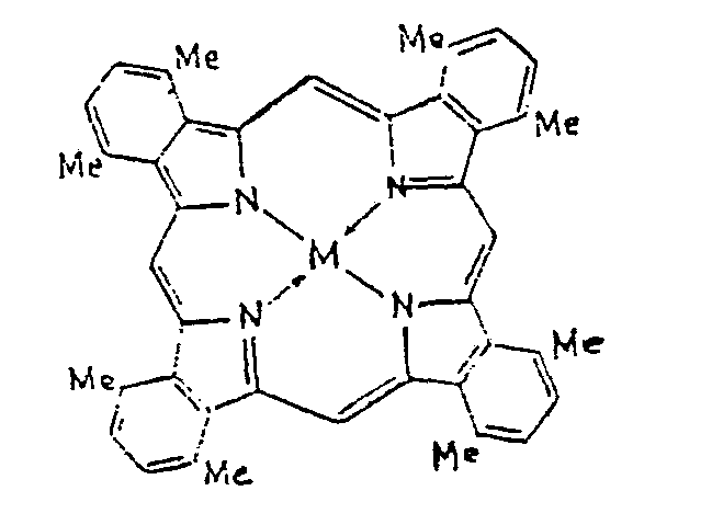
- aus der Gruppe der Porphyrine und deren Derivate mit der allgemeinen Strukturformel
- Der zuvor angegebene π-Donor-Bestandteil bildet in Gegenwart von Halogen leitende Ladungsübertragungszusammensetzungen nach der nachfolgenden Reaktionsgleichung :

- Es ist allgemein bekannt, daß zum Erhalt hoher Leitfähigkeit das stöchiometrische Verhältnis (d. h. n in der obigen Gleichung) des Ladungsübertragungssalzes kleiner als 1 sein muß. Der Wert von n kann im allgemeinen in einem Bereich zwischen 0 und 1 variieren, ohne daß die leitenden Eigenschaften wesentlich beeinflußt werden.
- Es wurde gefunden, daß die zuvor angegebenen Ladungsübertragungssalze die Basis eines neuen lithographischen Verfahrens bilden. Dieses Verfahren basiert auf der Feststellung, daß bei Bestrahlung des Ladungsübertragungssalzes mit einem Elektronenstrahl entsprechender Energiedichte ein Verlust des Halogens in dem Ladungsübertragungssalz in den bestrahlten Bereichen stattfindet; d. h., der Elektronenstrahl bewirkt die Umkehr einer Ladungsübertragungsreaktion gemäß der nachfolgenden Gleichung :

- Im allgemeinen können diese Ladungsübertragungssalze durch Sublimation abgeschieden werden. Dabei werden glatte, festhaftende und glasartige Filme erhalten. Filme mit einer einheitlichen Schichtdicke im Bereich von 300 nm bis 2 µm oder darüber konnten auf diese Art und Weise abgeschieden werden. In den Fällen, in denen das Salz einen niedrigen Dampfdruck hat oder thermisch instabil ist, können die Filme durch Lösungsbeschichtungstechnologie hergestellt werden.
- Es wurde weiterhin festgestellt, daß mit diesen Materialien sowohl negative wie auch positive Resistbilder hergestellt werden können. Der Bildmodus hängt von den Parametern des Elektronenstrahls ab, d. h. von seiner Energie und Ladungsdichte. Beispielsweise liegt für negative Bilder die Elektronenstrahlenergie in einem Bereich von 8,01 - 10-19 bis 48,06 10-19 Joule. Die Ladungsdichte liegt in einem Bereich von unter 10-3 bis 10-4 C/cm2. Die Bestrahlung erfolgt bei Zimmertemperatur. Die Bilder werden in geeigneten polaren Lösungsmitteln wie kurzkettigen Alkoholen, Wasser, Dimethylformamid, Dimethylsulfoxid, Acetonitril und dergleichen entwickelt.
- In dem negativen Bild findet eine Vernetzungsreaktion statt unter Erhalt der gewünschten Muster, die in heißen Lösungsmitteln nicht mehr verändert werden. Beispielsweise wurde ein negatives Bild, das in einem Film aus Tetrathiofulvalenbromid hergestellt wurde, durch Behandlung in kochendem Chlorbenzol, Dimethylsulfoxid und dergleichen nicht mehr verändert. Das Bild wurde auch Temperaturen von 275 °C im Vakuum bei 1,33 x 10⁻⁹ bar unterworfen, wobei ebenfalls keine Veränderung eintrat. Die Bilder lassen sich leicht durch eine 1 bis 2 Minuten dauernde Behandlung mit wässrigem Hydrazin bei Zimmertemperatur entfernen. Die negativen Resistbilder haben Dimensionen von weniger als 1 µm, weisen eine ausgezeichnete Kantendefinition von 0,1 µm auf, und es können nahezu vertikale Seitenwände erhalten werden. Es fand kein Aufquellen der Bilder statt, wenn diese mit einer Vielzahl polarer und nichtpolarer Lösungsmittel behandelt wurden.
- Positive Resistbilder können entweder in situ oder durch Lösungsmittelentwicklung hergestellt werden. Bei dem in situ-Verfahren wird der Resist mit einem Elektronenstrahl mit einer Ladungsdichte im Bereich von über 10-3 bis 10-1 C/cm2 und einer Energie von 8,01 10-19 bis 48,06 10-19 Joule bestrahlt. Bei diesen Ladungsdichteniveaus verdampfen die bestrahlten Resistmaterialien. Diese Sublimation kann noch durch Erhitzen der Unterlagen, auf denen sich der Resist befindet, auf Temperaturen im Bereich von 60 bis 100°C verstärkt werden.
- Mit Lösungsmittel entwickelte, positive Bilder werden in denjenigen Fällen erhalten, in denen die Ladungsübertragungssalze nicht ohne weiteres verdampfen bei der Bestrahlung und nach dem Halogenverlust. Daß bei der Bestrahlung ein Halogenverlust stattfindet, wird mit der Elektronenmikrosonden-Technologie festgestellt. Die bestrahlten Materialien sind leicht mit schwach polaren Lösungsmitteln wie Methylenchlorid, Chloroform, Kohlenstofftetrachlorid und dgl. entfernbar. Der Vorteil der Lösungsmittelentwicklung liegt darin, daß im Prinzip empfindlichere, positive Resistmaterialien angewendet werden können. Ein weiteres Merkmal der Lösungsmittelentwicklung ist, daß weniger flüchtige Donoren im Bildbeschichtungsprozeß eingesetzt werden können.
- Es konnte auch festgestellt werden, daß die bestrahlten und nicht bestrahlten Materialien gemäß der Erfindung verschiedene elektrische und optische Eigenschaften aufweisen. Es war bekannt, daß die nicht bestrahlten Filme hochleitend waren mit Leitfähigkeiten im Bereich von 0,1 bis 20/Ohm-cm. Diese Leitfähigkeit ist von praktischem Vorteil, weil durch sie der Aufbau statischer Ladungen in dem Film während der Bestrahlung vermieden wird. Bei bisher bekannten isolierenden Polymerresistmaterialien mußte deswegen ein dünner metallischer Überzug auf dem Resist abgeschieden werden. Mit den vorliegenden Materialien ist dies nicht mehr erforderlich. Während der nichtbestrahlte Bereich hohe Leitfähigkeit aufweist, wurde gefunden, daß der bestrahlte resist isolierend ist. Es wurde beispielsweise gefunden, daß ein Film aus Tetrathiofulvalenbromid ; der auf eine Unterlage durch Sublimation aufgetragen wurde und dessen Leitfähigkeit gemessen und mit der eines entwickelten negativen Elektronenstrahlbildes verglichen wurde, eine Änderung der Leitfähigkeit um 8 Größenordnungen oder darüber aufwies. Der nichtbestrahlte Resist zeigte eine Leitfähigkeit von 20/Ohm-cm, während die bestrahlten Bereiche eine Leitfähigkeit von weniger als 10-7/Ohm-cm aufwiesen.
- Es wurde auch beobachtet, daß große Änderungen der optischen Eigenschaften in den bestrahlten Bereichen des Resists auftraten. Es wurde beobachtet, daß die nichtbestrahlten Resistfilme stark im sichtbaren und im nahen Infrarotbereich Licht absorbieren, während die bestrahlten Filme in diesen Bereichen keine Absorptionen aufwiesen. Beispielsweise wurde gefunden, daß Tetrathiofulvalenbromidfilme starke Absorptionen bei 550 und bei 380 nm aufwiesen. Nach der Bestrahlung ergaben optische Messungen, daß diese Absorptionen in den bestrahlten Bereichen nicht mehr vorhanden waren. Es sollte hevorgehoben werden, daß eine Entwicklung nicht erforderlich ist, um optisch die mit Elektronenstrahl eingeschriebenen Muster in den vorliegenden Filmen feststellen zu können. Die optische Absorption hängt natürlich auch von der Zusammensetzung ab. Beispielsweise absorbieren Ladungsübertragungssalze von Tetrathiotetracen und Tetraphenyldithiodipyran stark im Bereich von 800 bis 850 nm. Der Unterschied in der Lichtabsorption nichtbestrahlter Materialien gegenüber bestrahlten Materialien gestattet die Anwendung der Materialien als optische Masken und in Video-Speichervorrichtungen.
- Die Empfindlichkeit des lithographischen Verfahrens und die optischen und elektrischen Eigenschaften der erfindungsgemäßen Resistmaterialien sind von dem entsprechenden Halogengehalt und den Parametern des Elektronenstrahls abhängig.
- Es wurde gefunden, daß eine Empfindlichkeitssteigerung bei der Umkehr der Ladungsübertragungsreaktion stattfindet, wenn man vom Tetrathiofulvalenbromid zu dem entsprechenden Chlord übergeht. Durch diesen Übergang findet eine Empfindlichkeitssteigerung um einen Faktor größer 5 statt. In einem anderen Beispiel wird ein Film aus einem neutralen Donor abgeschieden und dann mit Halogen behandelt unter Erhalt eines Ladungsübertragungssalzes mit einem kleineren molaren Gehalt an Halogen. Bei Elektronenbestrahlung dieses Materials ist daher weniger. Halogen zu entfernen, was zu einer entsprechenden Steigerung der Empfindlichkeit führt.
- Die Erfindung wird anhand der nachfolgenden Ausführungsbeispiele näher erläutert.
- Es wird ein Film aus Tetrathiofulvalenbromid (TTF-Brn) mit einer Schichtdicke von 500 nm durch Vakuumsublimation von TTF-Brn bei einem Druck von 111m und bei einer Temperatur von 185 bis 190 °C hergestellt. Die Sublimation wird für 10 Minuten aufrecht erhalten. Die Analyse des so hergestellten Films zeigte eine nichtstöchiometrische Zusammensetzung von TTF-Bro.78.
- Es wird ein Bild in diesem Film hergestellt, indem man einen Elektronenstrahl in einem vorbestimmten Muster auftreffen läßt. Der Elektronenstrahl hatte eine Stromdichte von 10-4 C/cm2 und eine Energie von 10 keV. Der Film wird dann 15 Sekunden lang bei Zimmertemperatur mit Methanol gewaschen, um die nichtbelichteten Bereiche des Films zu entfernen. Es blieb ein negatives Resistbild mit Dimensionen kleiner 1 11m zurück. Dieses Bild bleibt unverändert, wenn es kochendem Chlorbezol oder Dimethylsulfoxid ausgesetzt wurde oder im Vakuum auf 275 °C erhitzt wurde. Es wird jedoch entfernt, wenn es mit wässriger Hydrazinlösung 1 bis 2 Minuten lang bei Zimmertemperatur behandelt wird.
- An dem Film wurden vor und nach der Bestrahlung optische und Leitfähigkeitsmessungen durchgeführt. Vor der Bestrahlung wies der Film die charakteristischen TTF-Br-Salz Absorptionen bei 550 und 380 nm auf. Nach der Bestrahlung fehlten diese Absorptionen. In ähnlicher Weise betrug die Leitfähigkeit des Films 20/Ohm-cm vor der Bestrahlung und danach kleiner 10-7/Ohm-cm.
- Ein Film von TTF-Br0,78 wird wie in Beispiel 1 angegeben hergestellt. Der Film wird in einem vorbestimmten Muster mit einem Elektonenstrahl mit einer Stromdichte von 10-3 C/cm2 und einer Energie von 10 KeV bestrahlt. Nach der Bestrahlung wurde gefunden, daß der beaufschlagte Film entfernt war unter Erhalt eines positiven Resistbildes. Das Bild zeigte Dimensionen kleiner 1 11m mit nahezu vertikalen Seitenwänden. Eine weitere Entwicklung ist nicht erforderlich.
- Ein Film aus Tetrathiofulvalenchlorid (TTF-Cl0,65) wird wie in Beispiel 1 angegeben hergestellt, mit der Ausnahme, daß eine Badtemperatur von 195 bis 205 °C angewendet wird. Die Stöchiometrie des Films betrug TTF-Cl0,65. Der Film wird bestrahlt und anschließend, wie in Beispiel 1 angegeben, zu einem negativen Bild entwickelt. Es wurde gefunden, daß die Löslichkeit, die optischen und elektrischen Eigenschaften dem Film, der in Beispiel 1 abgeschieden wurde, ähneln. Es wurde weiterhin gefunden, daß der TTF-Cl0,65-Film etwa 5 mal empfindlicher als der TTF-BR0,78-Film von Beispiel 1 ist.
- Ein Film aus TTF-Cl0,65 wird, wie in Beispiel3 angegeben, hergestellt und wie in Beispiel 2 angegeben bestrahlt und behandelt. Es wird ohne Lösungsmittelentwicklung ein positives Resistbild erhalten. Das Bild weist Dimensionen kleiner 1 µm mit nahezu vertikalen Wänden auf.
- Ein Film aus Tetrathiofulvalenjodid (TTF-Jn) wird hergestellt nach dem Verfahren von Beispiel 1 mit der Ausnahme, daß auf eine Temperatur von 140 bis 150 °C erhitzt wird. Die Analyse des Films ergab eine Stöchiometrie von TTF-JO.7. Der Film wird bestrahlt und anschließend behandelt wie analoge Filme in den Beispielen 1 und 2 unter Erhalt negativer und positiver Resistbilder. Die Löslichkeit, die optischen und elektrischen Eigenschaften ähneln denen der Filme gemäß den Beispielen 1 und 2.
- Ein Film aus Tetraselenofulvalenbromid (TSeF-Brn) wird wie in Beispiel 1 angegeben, hergestellt, und es wird eine Filmzusammensetzung von TSeF-Bro.8 erhalten. Dieser Film wird bestrahlt und anschließend behandelt wie in den Beispielen 1 und 2 unter Erhalt der entsprechenden negativen und positiven Resistbilder. Optische Messungen ergaben, daß der nichtbestrahlte Film starke Absorptionen bei 430 und 650 nm aufwies. Ähnliche Änderungen in der Löslichkeit, den optischen und elektrischen Eigenschaften wie in Beispiel 1 wurden beobachtet.
- Tetrathiotetracen (TTT) wird im Vakuum bei 1 m und 350 °C sublimiert unter Erhalt eines neutralen TTT-Films. Der Film wird dann etwa 10 Minuten lang einem Bromdampf ausgesetzt, wodurch ein leitender Film mit der Stöchiometrie TTT-Bro erhalten wird. Dieser Film wird bestrahlt und behandelt wie in den Beispielen 1 und 2, wodurch negative und positive Resistbilder mit ähnlichen Änderungen der elektrischen Eigenschaften wie in den vorherigen Beispielen erhalten werden.
- Es können auch Halogensalze der nachfolgenden Materialien in ähnlicher Weise als Elektronenstrahl-Resistmaterialien eingesetzt und behandelt werden wie in den zuvor beschriebenen Beispielen :
- Diselenodithiofulvalen,
- Dimethyltetrathiofulvalen,
- Dimethyltetraselenofulvalen,
- Dimethyldiselenodithiofulvalen,
- Tetramethyltetrathiofulvalen,
- Tetramethyltetraselenofulvalen,
- Tetramethyldiselenodithiofulvalen,
- Hexamethylentetrathiofulvalen,
- Hexamethylentetraselenofulvalen,
- Hexamethylendiselenodithiofulvalen,
- Tetrathionaphthalin,
- Tetraselenonaphthalin,
- Perylen,
- Dithiodipyran,
- Tetramethyldithiodipyran,
- Tetraphenyldithiodipyran,
- Diselenodipyran,
- Tetramethyldiselenodipyran,
- Tetraphenyldiselenodipyran,
- Dipyran,
- Tetramethylphenylendiamin,
- Phthalocyanin,
- Nickel-, Kupfer-, Kobalt-, Eisen-phthalocyanin,
- Octamethyltetrabenzporphyrin,
- Nickel-octamethyltetrabenzporphyrin.
- In der vorliegenden Erfindung wird die Verwendung einer Klasse von Resistmaterialien beschrieben, die allgemein als leitende organische Ladungsübertragungssalze klassifiziert werden können. Mit diesen Materialien können sowohl negative wie auch positive Resistbilder nur durch Kontrolle der Bestrahlungsparameter, d. h. der Energie und der Stromdichte hergestellt werden. Die Resistmaterialien weisen weiter Vorteile auf, beispielsweise große Unterschiede in der Löslichkeit, in den optischen und elektrischen Eigenschaften, die aus der Bestrahlung resultieren. Diese Eigenschaften machen die Materialien für die Herstellung von Mikrostrukturen für elektronische Schaltkreise mit hoher Integrationsdichte, für die Verwendung als optische Speichermedien und zur Herstellung von Maskenvorlagen für die Photolithographie geeignet. Außerdem findet eine Eliminierung statischer Ladungen in dem Resist während der Elektronen- oder lonenbestrahlung statt.
Claims (15)


in denen das stöchiometrische Verhältnis des Ladungsübertragungssalzes kleiner 1 ist, als elektronenstrahlempfindliches Resistmaterial.
Applications Claiming Priority (2)
| Application Number | Priority Date | Filing Date | Title |
|---|---|---|---|
| US6529179A | 1979-08-09 | 1979-08-09 | |
| US65291 | 1979-08-09 |
Publications (3)
| Publication Number | Publication Date |
|---|---|
| EP0023988A2 EP0023988A2 (de) | 1981-02-18 |
| EP0023988A3 EP0023988A3 (en) | 1982-01-20 |
| EP0023988B1 true EP0023988B1 (de) | 1984-02-29 |
Family
ID=22061674
Family Applications (1)
| Application Number | Title | Priority Date | Filing Date |
|---|---|---|---|
| EP80104214A Expired EP0023988B1 (de) | 1979-08-09 | 1980-07-18 | Verwendung eines leitenden organischen Ladungsübertragungsmaterials als elektronenstrahlempfindliches Resistmaterial und Verfahren zur Herstellung positiver und negativer Resistbilder |
Country Status (5)
| Country | Link |
|---|---|
| EP (1) | EP0023988B1 (de) |
| JP (1) | JPS5627139A (de) |
| CA (1) | CA1165761A (de) |
| DE (1) | DE3066749D1 (de) |
| IT (1) | IT1149813B (de) |
Families Citing this family (8)
| Publication number | Priority date | Publication date | Assignee | Title |
|---|---|---|---|---|
| US4522754A (en) * | 1982-11-12 | 1985-06-11 | Ciba Geigy Corporation | Metallically conducting (2-fluoro-5,6,11,12-tetraselenotetracene)2 -bromide |
| US4601853A (en) * | 1984-02-13 | 1986-07-22 | Ciba-Geigy Corporation | (2-fluoro-5,6,11,12-tetraselenotetracene)2 chloride |
| CH664963A5 (de) * | 1985-10-18 | 1988-04-15 | Ciba Geigy Ag | Difluorierte (5,6,11,12-tetraselenotetracen)2-halogenide, verfahren zu deren herstellung und deren verwendung. |
| JPS6435545A (en) * | 1987-07-31 | 1989-02-06 | Japan Synthetic Rubber Co Ltd | Resist composition used for processing with charged particle beam |
| JPH01210944A (ja) * | 1988-02-18 | 1989-08-24 | Japan Synthetic Rubber Co Ltd | 感放射線性樹脂組成物 |
| EP0362143B1 (de) * | 1988-09-30 | 1995-11-15 | Ciba-Geigy Ag | Antistatische und elektrisch leitende Reliefbilder, Verfahren zu deren Herstellung, Beschichtungsmittel und strahlungsempfindliche Polymere |
| JP5458267B2 (ja) * | 2009-02-24 | 2014-04-02 | 国立大学法人東京工業大学 | ヘキサメチレンテトラチアフルバレン化合物、有機半導体および有機薄膜トランジスタ |
| CN113004291B (zh) * | 2019-12-20 | 2022-03-01 | 中国科学院化学研究所 | 基于金属卟啉的分子玻璃化学放大光刻胶及其制备方法和应用 |
Family Cites Families (2)
| Publication number | Priority date | Publication date | Assignee | Title |
|---|---|---|---|---|
| US3925076A (en) * | 1971-02-16 | 1975-12-09 | Monsanto Co | Light sensitive compositions and products |
| US4312991A (en) * | 1979-05-10 | 1982-01-26 | International Business Machines Corporation | Dithiobenzoate 4,5-dicyano-1,3-(dithiolidene-2-yl)methylene |
-
1980
- 1980-06-09 JP JP7677080A patent/JPS5627139A/ja active Granted
- 1980-06-16 CA CA000354062A patent/CA1165761A/en not_active Expired
- 1980-07-18 DE DE8080104214T patent/DE3066749D1/de not_active Expired
- 1980-07-18 IT IT23528/80A patent/IT1149813B/it active
- 1980-07-18 EP EP80104214A patent/EP0023988B1/de not_active Expired
Also Published As
| Publication number | Publication date |
|---|---|
| CA1165761A (en) | 1984-04-17 |
| IT1149813B (it) | 1986-12-10 |
| JPS6245969B2 (de) | 1987-09-30 |
| IT8023528A0 (it) | 1980-07-18 |
| DE3066749D1 (en) | 1984-04-05 |
| EP0023988A2 (de) | 1981-02-18 |
| JPS5627139A (en) | 1981-03-16 |
| EP0023988A3 (en) | 1982-01-20 |
Similar Documents
| Publication | Publication Date | Title |
|---|---|---|
| EP0000702B1 (de) | Verfahren zur Herstellung einer fliessbeständigen Resistmaske aus strahlungsempfindlichem Resistmaterial | |
| DE69816601T2 (de) | Konjugierte polymer in einem oxidierten zustand | |
| US4312935A (en) | Class of E-beam resists based on conducting organic charge transfer salts | |
| DE1118004B (de) | Elektrophotographisches Verfahren mit elektrolytischer Bildentwicklung | |
| DE2519403A1 (de) | Traegermaterial und dessen verwendung in einem photographischen aufzeichnungsmaterial | |
| DE3241980A1 (de) | Verfahren zur erzeugung eines metallischen bildes sowie verbundmaterial und behandlungsloesung dafuer | |
| DE2728352C2 (de) | ||
| DE2627828C2 (de) | Verfahren zur Herstellung eines elektrisch leitenden Bildes | |
| DE3903421A1 (de) | Elektrisch leitfaehige resistmasse, verfahren zu ihrer herstellung und ihre verwendung | |
| EP0023988A2 (de) | Verwendung eines leitenden organischen Ladungsübertragungsmaterials als elektronenstrahlempfindliches Resistmaterial und Verfahren zur Herstellung positiver und negativer Resistbilder | |
| DE2743763A1 (de) | Positivlackmaterial und verfahren zur herstellung einer lackmaske | |
| DE2724160A1 (de) | Bildaufzeichnungsmaterial | |
| DE69021119T2 (de) | Bildherstellungsverfahren mittels einer elektrisch leitfähigen Zusammensetzung. | |
| DE2723613C2 (de) | ||
| DE2711717A1 (de) | Ionen-radikalsalze, verfahren zu ihrer herstellung sowie aus den salzen hergestellte elemente | |
| DE1643765A1 (de) | Strahlungsempfindliches Material | |
| DE1597891A1 (de) | Verfahren zur Bilderzeugung | |
| US4338392A (en) | Class of E-beam resists based on conducting organic charge transfer salts | |
| DE3411714A1 (de) | Verfahren zur herstellung von polyimidazol- und polyimidazopyrrolon-reliefstrukturen | |
| DE3889967T2 (de) | Mikrolithographisches Verfahren zur Herstellung von Schaltungen unter Verwendung von für elektromagnetische Strahlungen und geladene Teilchen empfindlichen organischen leitfähigen Filmen. | |
| DE1289426B (de) | Verfahren zum Fixieren von Bildern in einer Schicht aus photochromen stickstoffhaltigen Spiropyranverbindungen | |
| DE2702947A1 (de) | Verfahren zum elektrostatischen drucken | |
| DE2652252C2 (de) | Elektrophotographisches Verfahren zur Herstellung einer flexiblen Flachdruckform | |
| DE2425286B2 (de) | Verfahren zum herstellen eines elektrophotographischen aufzeichnungsmaterials | |
| DE2441263A1 (de) | Aufzeichnungsverfahren |
Legal Events
| Date | Code | Title | Description |
|---|---|---|---|
| PUAI | Public reference made under article 153(3) epc to a published international application that has entered the european phase |
Free format text: ORIGINAL CODE: 0009012 |
|
| AK | Designated contracting states |
Designated state(s): DE FR GB |
|
| 17P | Request for examination filed |
Effective date: 19810807 |
|
| PUAL | Search report despatched |
Free format text: ORIGINAL CODE: 0009013 |
|
| AK | Designated contracting states |
Designated state(s): DE FR GB |
|
| GRAA | (expected) grant |
Free format text: ORIGINAL CODE: 0009210 |
|
| AK | Designated contracting states |
Designated state(s): DE FR GB |
|
| REF | Corresponds to: |
Ref document number: 3066749 Country of ref document: DE Date of ref document: 19840405 |
|
| ET | Fr: translation filed | ||
| PLBE | No opposition filed within time limit |
Free format text: ORIGINAL CODE: 0009261 |
|
| STAA | Information on the status of an ep patent application or granted ep patent |
Free format text: STATUS: NO OPPOSITION FILED WITHIN TIME LIMIT |
|
| 26N | No opposition filed | ||
| PGFP | Annual fee paid to national office [announced via postgrant information from national office to epo] |
Ref country code: GB Payment date: 19900531 Year of fee payment: 11 |
|
| PGFP | Annual fee paid to national office [announced via postgrant information from national office to epo] |
Ref country code: FR Payment date: 19900626 Year of fee payment: 11 |
|
| PGFP | Annual fee paid to national office [announced via postgrant information from national office to epo] |
Ref country code: DE Payment date: 19900730 Year of fee payment: 11 |
|
| PG25 | Lapsed in a contracting state [announced via postgrant information from national office to epo] |
Ref country code: GB Effective date: 19910718 |
|
| GBPC | Gb: european patent ceased through non-payment of renewal fee | ||
| PG25 | Lapsed in a contracting state [announced via postgrant information from national office to epo] |
Ref country code: FR Effective date: 19920331 |
|
| PG25 | Lapsed in a contracting state [announced via postgrant information from national office to epo] |
Ref country code: DE Effective date: 19920401 |
|
| REG | Reference to a national code |
Ref country code: FR Ref legal event code: ST |