EP0019366A2 - Vorrichtung zur Steuerung der Darstellung von Cursoren bei einem Anzeigesystem mit Raster-Abtastung - Google Patents
Vorrichtung zur Steuerung der Darstellung von Cursoren bei einem Anzeigesystem mit Raster-Abtastung Download PDFInfo
- Publication number
- EP0019366A2 EP0019366A2 EP80301264A EP80301264A EP0019366A2 EP 0019366 A2 EP0019366 A2 EP 0019366A2 EP 80301264 A EP80301264 A EP 80301264A EP 80301264 A EP80301264 A EP 80301264A EP 0019366 A2 EP0019366 A2 EP 0019366A2
- Authority
- EP
- European Patent Office
- Prior art keywords
- information
- address
- cursor
- display
- raster
- Prior art date
- Legal status (The legal status is an assumption and is not a legal conclusion. Google has not performed a legal analysis and makes no representation as to the accuracy of the status listed.)
- Granted
Links
Images


Classifications
-
- G—PHYSICS
- G09—EDUCATION; CRYPTOGRAPHY; DISPLAY; ADVERTISING; SEALS
- G09G—ARRANGEMENTS OR CIRCUITS FOR CONTROL OF INDICATING DEVICES USING STATIC MEANS TO PRESENT VARIABLE INFORMATION
- G09G5/00—Control arrangements or circuits for visual indicators common to cathode-ray tube indicators and other visual indicators
- G09G5/08—Cursor circuits
-
- G—PHYSICS
- G09—EDUCATION; CRYPTOGRAPHY; DISPLAY; ADVERTISING; SEALS
- G09G—ARRANGEMENTS OR CIRCUITS FOR CONTROL OF INDICATING DEVICES USING STATIC MEANS TO PRESENT VARIABLE INFORMATION
- G09G1/00—Control arrangements or circuits, of interest only in connection with cathode-ray tube indicators; General aspects or details, e.g. selection emphasis on particular characters, dashed line or dotted line generation; Preprocessing of data
- G09G1/007—Circuits for displaying split screens
Definitions
- the present invention relates to a display system and, more particularly, to a display system of the type in which a screen of a display system of the raster scan type is divided into a plurality of sections and the display information on the screen divided are supplied to stations by using mirror reflection.
- a Key to FDD (referred to as a data system) using a floppy disc as a recording medium has been used widely.
- FDD is an abbreviation of a floppy disc drive.
- a data system of this type allowing two operators to individually perform the works has an increasing market because of its good cost/performance.
- the two-operator data system will be called a multiple data system.
- Most of the multiple data system is of the type using a single display unit. More particularly, a single screen is divided into two screen sections for displaying independently the display information. A mirror used in combination with the divided-screen reflects the display information on the divided screens toward two operators.
- the display unit may be single but the display controller can not be reduced to 1/2 in the hardware, simply. Especially, one cursor signal is necessary for the respective operators. Accordingly, the number of parts used in the cursor control circuit increases to make the circuit complicated and cost thereof high.
- an object of the invention is to provide a cursor display system capable of displaying cursors at different positions on the display surface of stations.
- a * display system which divides display screen and provides display information to respective sides using mirror reflection comprising;
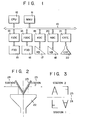
- a main memory unit (MMU) 11 connecting to a system bus 10 including an address line, a data line and a control line is comprised of a read only memory and a random access memory and stores programs and data through the system line 10.
- a central processing unit (CPU) 12 connecting to the system bus 10 performs arithmetic operation and the control of the entire system under control of the program stored in the MMU 11.
- Floppy disc controllers (FDD) 13 and 14 are connected to the system bus 10 and also to floppy disc units (FDU) 15 and 16.
- the FDUs 15 and 16 store the programs and data which are overflowed from the MMU 11.
- the keyboards 17 and 18 are connected through keyboard controllers (KBC) 19 and 20 to the system bus 10.
- KBC keyboard controllers
- the data keyed in by the KBS 17 and 18 are temporarily stored in the MMU 11 through the system bus 20 and then is displayed on the CRT 22 through the CRT controller 21 (CRTC).
- the CRTC 21 holds the display data of the CRT 22, performs the data conversion, and generates the synchronizing signal.
- the CRT 22 is so designed as to provide two picture screens corresponding to the stations.
- the FDD 15 and the KB 17 are assigned to the station 1 or the FDD 16 and the KB 18 are assigned to the station 2.
- Fig. 2 illustrates the principle to provide two pictures by using a single picture screen.
- Pictures on the CRT 22 are reflected by a mirror 23 toward the operators at the stations #1 24 and #2 25.
- one picture screen is divided into two sections and the different information are supplied to the respective operators. Accordingly, when characters "F" and "A" as the display data are applied to the stations, the formats of the characters displayed on the CRT screen are as shown in Fig. 3 and the upper part above a central broken line is for the station #2 25 and the lower part below the broken line is for the station #1 24.
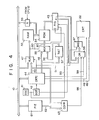
- Fig. 4 is a hardware block diagram of an embodiment of a cursor control system according to the invention.
- an oscillator 41 produces a clock signal to provide dots which cooperatively form a symbol or characters on the CRT screen.
- a dot counter 42 is connected to the oscillator 41 to count the clock signal produced from the oscillator 41 and to produce the count data for each character display.
- the counter data outputted is supplied to a CRT controller 44 and a bidirectional shift register 43.
- the CRT controller 44 is connected to the system bus 10 and the dot counter 42.
- the CRT controller 44 is a controller for interfacing between the CPU 12 and the CRT 22 of the raster scan type.
- HD 46505 Programmable CRT Controller
- LSI large scale integration
- the controller 44 is capable of controlling of: the period of the horizontal scanning, the period of the vertical scanning for each line, the number of display characters for each line, the number of display lines of one picture, the number of rasters for each line, the display position in the horizontal direction on the CRT 22, the display position in the vertical direction on the CRT, the pulse width of a horizontal synchronizing signal, the cursor display position on the CRT 22, and the direction of an address to make an access to the refresh memory. Accordingly, the CRT controller 44 can programmably form a picture on the CRT 22 using the above items as parameters.
- the CRT controller 44 has four registers--for signals to control the cursor.
- Those registers are: a cursor start raster register, a cursor end raster register, a cursor (H) register to store the high portion of the refresh memory address, and a cursor (L) register to store the low portion of the refresh memory address. If the capacity of the refresh memory is small, for example, 256 words/display, a parameter is set only in the cursor (L) resistor. In the cursor (H) register, all "ZERO" should be set. In this case, however, the number of bits are 8 bits.
- the controller 44 produces a horizontal synchronizing signal through a line 48 and a vertical synchronizing signal through a line 49 for transmission for the CRT 22.
- the same supplies a display timing signal through a line 51 to a multiplexer 47 and an AND circuit 47, through a line 51.
- the cursor display signal is supplied to an OR circuit 58, through a line 59.
- the refresh memory address is supplied through a bus line 45 to the multiplexer 47 and a comparator 63.
- the raster address is supplied to a multiplexer 55 and a raster address converting circuit 57 through a bus line 46.
- the multiplexer 47 receives an address from the system bus 10 and a refresh memory address signal for reading which is outputted from the CRT controller 44, and selectively produces either of those.
- an address supplied through the system bus 10 is a write address used when display data is written into the refresh memory (RM1) 52.
- the address inputted from the CRT controller 44 is a read out address for reading out the display data from the refresh memory 52.
- the refresh memory (RAM) 52 is connected to the multiplexer 47 and is connected to the system bus 10 through a gate 53.
- the refresh memory 52 is comprised of a random access memory and stores the display information of one picture, for example, 1024 characters. Address information inputted through the multiplexer 47 reads out coded data from the refresh memory 52 and applies it to a character generator 54.
- the gate 53 is a control gate for applying the display data coming through the system bus 10 to the refresh memory 52, in response to the write signal from the CPU 12.
- the character generator 54 as a read only memory, is connected to the refresh memory 52 and a multiplexer 55.
- the character generator 54 converts the coded data into corresponding character information in response to the address information which is the combination of the display data and the raster address inputted from the CRTC 44 through the multiplexer 55.
- the multiplexer 55 connecting to the CRT controller 44 is supplied with raster address converting information applied through a bus line 46 and a raster address through the bus line 56.
- the multiplexer 55 is supplied with the most significant bit information outputted from the multiplexer 47, through a line 60.
- the same information is applied to the bidirectional shift register 43.
- the multiplexer 55 selects and produces the raster address through the bus line 46.
- the multiplexer 55 selects and produces the raster address converting information.
- the bidirectional shift register 43 when the most significant bit of the address is logical "0”, the display information is shifted to the right.
- the display information is shifted to the left.
- the raster address converting circuit 57 is comprised of an inverter and is connected to the CRT controller 44. The raster address converting circuit 57 inverts the raster address information supplied from the CRT controller 44 and the converted one is supplied to the multiplexer 55.
- the bidirectional shift register 43 is connected to the oscillator circuit 41, the dot counter 42, and the character generator 54. Having the output signal from the dot counter the shift register 43 fetches the character pattern information from the character generator 54 and responds to the signal outputted from the oscillator circuit 41 to shift its contents to the right or to the left. The selection of the right shift or the left shift depends on the control signal (the most significant bit of the address information of the refresh memory 52) outputted from the multiplexer 47. When the most significant bit (MSB) is logical "0”, it is shifted to the right, for example, and when the MSB is logical "I", it is shifted to the left. The inverse shift direction in this case is of course allowed, if necessary.
- the OR circuit 58 is supplied with a cursor display signal from the CRT controller 44.
- the OR circuit 58 is connected to the AND circuit 67.
- the AND circuit 67 is supplied with a display timing signal from the CRT controller 44 through the line 51.
- the programmable interface element (PIE) 61 is connected to one input terminal of the comparator 63 through line 62 and the comparator 63 is supplied at the other input refresh memory address from the CRT controller 44 through the line 45.
- the programmable interface element (PIE) 61 has an input/output interface function between the system bus 10 and the related periphery equipments (not shown).
- the data may be programmably inputted and outputted to and from the PIE 61 having buffers of 3 by therein. Those 3-byte buffers may be used corresponding to a cursor start raster address register, a cursor end raster address register, and a cursor register (H) or (L).
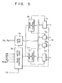
- It has three ports 71 to 73, as shown in Fig. 5. Those ports 71 to 73 have the functions changeable programmably.
- the port 71 has a single 8-bit data output latch/buffer and a single 8-bit data input latch.
- the port 72 has a single 8-bit data input, an output latch/buffer, and a single 8-bit input buffer.
- the port 73 has a single 8-bit data output latch/buffer, and a single 8-bit data input buffer (the input has no latch).
- the port 73 may be divided into ports 72 1 and 72 2 each of 4 bits by a mode control.
- Each 4-bit port is a 4-bit latch and is used for the output of the control signal or the input of the status information, in combination with the port 71 or the port 72.
- a data buffer 74 receives the control word from an internal data bus (not shown) under control of a command from the read/write control logic 75, the port control sections 76 and 77 produces commands to the ports designated.
- the programmable interface is constructed by 8255A sold by Intel Co. in U.S.A. and the operation and timing in each mode is described in "Intel 8080 Microcomputer System User's Manual” published by the same company on Sept., 1975.
- the comparator 63 compares the refresh memory address from the CRT controller 44 with the contents of the cursor address set in the buffer in the programmable interface element 61 and applies an output as a corresponding cursor signal to an OR gate 58.
- the AND gate 67 is conditioned by the output from the OR gate 58 and the display timing through the line 51 from the CRT controller 44 and applies an output signal as a video signal to the CRT 22.
- the output signal from the comparator 63 is coupled with the OR gate 58 through a control line 66.
- the output of the OR gate 58 is connected to one input terminal of an AND gate 67 of which other input terminal is connected to the CRT controller 44 through a control line 51.
- the output of the AND gate 67 is connected to the CRT 22.
- the CRT controller 44 includes a cursor start raster address register, a cursor end raster address register (not shown) and a cursor register (not shown), with relation to the invention.
- the former is for programming the end raster address of the cursor display and the start address of the cursor display, and the latter is for programming a current address to display the cursor.
- the latter register allows the read/write operation from the CPU 12.
- the cursor address programmed is compared with the internal address generated from an address generator (not shown) and a coincident signal is applied to the cursor control section (not shown).
- the cursor control section provides a cursor display signal which is a video signal for displaying a cursor on the CRT display screen. This signal is inhibited during a period of time that the display timing signal is logical "0". Normally, the signal is mixed with the character video signal and the mixed one is supplied to the CRT display unit.
- Fig. 6 is logic diagram of the bidirectional shift register 43 shown in Fig. 4.
- the embodiment employs an 8-bit parallel access right left shift register (SN74198 sold by Texas Instrument Co. in U.S.A. or the equirment).
- the shift register has all the functions required for the shift register, and has a parallel input, a parallel output, a right shift input, a left shift input, an operation mode control input and a direct clear input.
- an operation mode control input Sl or SO
- the following modes may be selected:
- the 8-bit data is applied to the inputs A to H and is stored in the respective floppy discs by clocking.
- the shift right mode the data is shifted to the right at the leading edge of the input clock pulse.
- the serial data is applied to the shift right terminal.
- the shift left mode the serial data applied to the shift left terminal is shifted to the left by the input clock pulse.
- logical "0" of signals SO and Sl is applied, as in the following table.
Landscapes
- Engineering & Computer Science (AREA)
- Physics & Mathematics (AREA)
- Computer Hardware Design (AREA)
- General Physics & Mathematics (AREA)
- Theoretical Computer Science (AREA)
- Radar, Positioning & Navigation (AREA)
- Remote Sensing (AREA)
- Controls And Circuits For Display Device (AREA)
Applications Claiming Priority (2)
| Application Number | Priority Date | Filing Date | Title |
|---|---|---|---|
| JP54051441A JPS5848106B2 (ja) | 1979-04-27 | 1979-04-27 | カ−ソル表示方式 |
| JP51441/79 | 1979-04-27 |
Publications (3)
| Publication Number | Publication Date |
|---|---|
| EP0019366A2 true EP0019366A2 (de) | 1980-11-26 |
| EP0019366A3 EP0019366A3 (en) | 1981-03-25 |
| EP0019366B1 EP0019366B1 (de) | 1983-05-25 |
Family
ID=12887008
Family Applications (1)
| Application Number | Title | Priority Date | Filing Date |
|---|---|---|---|
| EP80301264A Expired EP0019366B1 (de) | 1979-04-27 | 1980-04-18 | Vorrichtung zur Steuerung der Darstellung von Cursoren bei einem Anzeigesystem mit Raster-Abtastung |
Country Status (4)
| Country | Link |
|---|---|
| US (1) | US4323891A (de) |
| EP (1) | EP0019366B1 (de) |
| JP (1) | JPS5848106B2 (de) |
| DE (1) | DE3063429D1 (de) |
Cited By (3)
| Publication number | Priority date | Publication date | Assignee | Title |
|---|---|---|---|---|
| FR2517852A1 (fr) * | 1981-12-08 | 1983-06-10 | Telemecanique Electrique | Dispositif d'affichage double et application a un terminal d'enregistrement |
| FR2557713A1 (fr) * | 1983-12-06 | 1985-07-05 | Haure Jean Jacques | Micro-ordinateur a usage domestique comportant des possibilites d'affichage video, de lecture de clavier et de liaison a un magnetophone |
| EP0199123A3 (en) * | 1985-03-27 | 1989-04-26 | Ascii Corporation | Display controller |
Families Citing this family (11)
| Publication number | Priority date | Publication date | Assignee | Title |
|---|---|---|---|---|
| US4668947A (en) * | 1983-08-11 | 1987-05-26 | Clarke Jr Charles J | Method and apparatus for generating cursors for a raster graphic display |
| JPS60103906U (ja) * | 1983-12-20 | 1985-07-16 | 株式会社ヨコオ | アンテナ接続装置 |
| US4710763A (en) * | 1984-10-19 | 1987-12-01 | Texas Instruments Incorporated | Method for generating and displaying tree structures in a limited display area |
| DE3632601A1 (de) * | 1985-09-27 | 1987-04-23 | Olympus Optical Co | Vorrichtung zum darstellen einer positionsanzeigemarke auf mehreren bildschirmen |
| JPS6353634A (ja) * | 1986-08-25 | 1988-03-07 | Hitachi Ltd | 表示端末装置 |
| US5196839A (en) * | 1988-09-16 | 1993-03-23 | Chips And Technologies, Inc. | Gray scales method and circuitry for flat panel graphics display |
| US5285192A (en) * | 1988-09-16 | 1994-02-08 | Chips And Technologies, Inc. | Compensation method and circuitry for flat panel display |
| US5222212A (en) * | 1988-09-16 | 1993-06-22 | Chips And Technologies, Inc. | Fakeout method and circuitry for displays |
| US5018076A (en) * | 1988-09-16 | 1991-05-21 | Chips And Technologies, Inc. | Method and circuitry for dual panel displays |
| US5561811A (en) * | 1992-11-10 | 1996-10-01 | Xerox Corporation | Method and apparatus for per-user customization of applications shared by a plurality of users on a single display |
| US6061047A (en) * | 1996-09-17 | 2000-05-09 | Chips & Technologies, Inc. | Method and apparatus for clipping text |
Family Cites Families (5)
| Publication number | Priority date | Publication date | Assignee | Title |
|---|---|---|---|---|
| US3728710A (en) * | 1969-12-01 | 1973-04-17 | Hendrix Wire & Cable Corp | Character display terminal |
| US3792198A (en) * | 1972-09-28 | 1974-02-12 | Ibm | Partition system for image displays |
| US3777059A (en) * | 1972-10-30 | 1973-12-04 | Ibm | Multiple display device |
| JPS5827509B2 (ja) * | 1975-12-26 | 1983-06-09 | 株式会社日立製作所 | 画面分割制御装置におけるカ−ソル移動制御装置 |
| US4112423A (en) * | 1976-09-13 | 1978-09-05 | Kelsey-Hayes Co. | Dual-screen data display terminal for data processing units |
-
1979
- 1979-04-27 JP JP54051441A patent/JPS5848106B2/ja not_active Expired
-
1980
- 1980-04-18 DE DE8080301264T patent/DE3063429D1/de not_active Expired
- 1980-04-18 EP EP80301264A patent/EP0019366B1/de not_active Expired
- 1980-04-25 US US06/143,798 patent/US4323891A/en not_active Expired - Lifetime
Cited By (3)
| Publication number | Priority date | Publication date | Assignee | Title |
|---|---|---|---|---|
| FR2517852A1 (fr) * | 1981-12-08 | 1983-06-10 | Telemecanique Electrique | Dispositif d'affichage double et application a un terminal d'enregistrement |
| FR2557713A1 (fr) * | 1983-12-06 | 1985-07-05 | Haure Jean Jacques | Micro-ordinateur a usage domestique comportant des possibilites d'affichage video, de lecture de clavier et de liaison a un magnetophone |
| EP0199123A3 (en) * | 1985-03-27 | 1989-04-26 | Ascii Corporation | Display controller |
Also Published As
| Publication number | Publication date |
|---|---|
| EP0019366B1 (de) | 1983-05-25 |
| EP0019366A3 (en) | 1981-03-25 |
| DE3063429D1 (en) | 1983-07-07 |
| JPS55143587A (en) | 1980-11-08 |
| US4323891A (en) | 1982-04-06 |
| JPS5848106B2 (ja) | 1983-10-26 |
Similar Documents
| Publication | Publication Date | Title |
|---|---|---|
| US4228430A (en) | CRT Display apparatus with changeable cursor indicia | |
| US5592194A (en) | Display controller | |
| EP0019366B1 (de) | Vorrichtung zur Steuerung der Darstellung von Cursoren bei einem Anzeigesystem mit Raster-Abtastung | |
| US5652605A (en) | Display controller for a flat display apparatus | |
| US5146211A (en) | Bit mapped color cursor | |
| EP0054906B1 (de) | Anzeigevorrichtung | |
| US4356482A (en) | Image pattern control system | |
| JPS6049391A (ja) | ラスタ走査表示システム | |
| GB2179185A (en) | Interface device for converting the format of an input signal | |
| US4326201A (en) | Apparatus for displaying characters | |
| US5559533A (en) | Virtual memory hardware cusor and method | |
| JPS642955B2 (de) | ||
| US4272767A (en) | Display system for displaying information in the form of a horizontally oriented curve on a raster-type CRT | |
| US5635960A (en) | Horizontal position compensation circuit | |
| WO1989010609A1 (fr) | Unite de commande d'affichage | |
| US5055940A (en) | Video memory control apparatus | |
| US4384285A (en) | Data character video display system with visual attributes | |
| JPS63169687A (ja) | 表示装置 | |
| US4281393A (en) | Programmable computer terminal system | |
| US4965563A (en) | Flat display driving circuit for a display containing margins | |
| EP0123082B1 (de) | Anzeigegerät für logisches Zeitdiagramm | |
| EP0261629A2 (de) | Anzeigeeinrichtung | |
| KR920009762B1 (ko) | 단말기의 표시문자 제어장치 | |
| KR100329942B1 (ko) | 캐릭터표시제어회로 | |
| KR920001023Y1 (ko) | 멀티화면 기입 어드레스 제어회로 |
Legal Events
| Date | Code | Title | Description |
|---|---|---|---|
| PUAI | Public reference made under article 153(3) epc to a published international application that has entered the european phase |
Free format text: ORIGINAL CODE: 0009012 |
|
| 17P | Request for examination filed | ||
| AK | Designated contracting states |
Designated state(s): BE DE FR GB IT NL |
|
| PUAL | Search report despatched |
Free format text: ORIGINAL CODE: 0009013 |
|
| AK | Designated contracting states |
Designated state(s): BE DE FR GB IT NL |
|
| ITF | It: translation for a ep patent filed | ||
| GRAA | (expected) grant |
Free format text: ORIGINAL CODE: 0009210 |
|
| AK | Designated contracting states |
Designated state(s): BE DE FR GB IT NL |
|
| REF | Corresponds to: |
Ref document number: 3063429 Country of ref document: DE Date of ref document: 19830707 |
|
| ET | Fr: translation filed | ||
| PLBE | No opposition filed within time limit |
Free format text: ORIGINAL CODE: 0009261 |
|
| PLBE | No opposition filed within time limit |
Free format text: ORIGINAL CODE: 0009261 |
|
| STAA | Information on the status of an ep patent application or granted ep patent |
Free format text: STATUS: NO OPPOSITION FILED WITHIN TIME LIMIT |
|
| 26N | No opposition filed | ||
| 26N | No opposition filed | ||
| REG | Reference to a national code |
Ref country code: FR Ref legal event code: CD |
|
| REG | Reference to a national code |
Ref country code: GB Ref legal event code: 746 |
|
| ITTA | It: last paid annual fee | ||
| PGFP | Annual fee paid to national office [announced via postgrant information from national office to epo] |
Ref country code: GB Payment date: 19940408 Year of fee payment: 15 Ref country code: DE Payment date: 19940408 Year of fee payment: 15 |
|
| PGFP | Annual fee paid to national office [announced via postgrant information from national office to epo] |
Ref country code: FR Payment date: 19940411 Year of fee payment: 15 |
|
| PGFP | Annual fee paid to national office [announced via postgrant information from national office to epo] |
Ref country code: NL Payment date: 19940430 Year of fee payment: 15 |
|
| PGFP | Annual fee paid to national office [announced via postgrant information from national office to epo] |
Ref country code: BE Payment date: 19940607 Year of fee payment: 15 |
|
| PG25 | Lapsed in a contracting state [announced via postgrant information from national office to epo] |
Ref country code: GB Effective date: 19950418 |
|
| PG25 | Lapsed in a contracting state [announced via postgrant information from national office to epo] |
Ref country code: BE Effective date: 19950430 |
|
| BERE | Be: lapsed |
Owner name: TOKYO SHIBAURA DENKI K.K. Effective date: 19950430 |
|
| PG25 | Lapsed in a contracting state [announced via postgrant information from national office to epo] |
Ref country code: NL Effective date: 19951101 |
|
| GBPC | Gb: european patent ceased through non-payment of renewal fee |
Effective date: 19950418 |
|
| PG25 | Lapsed in a contracting state [announced via postgrant information from national office to epo] |
Ref country code: FR Effective date: 19951229 |
|
| NLV4 | Nl: lapsed or anulled due to non-payment of the annual fee |
Effective date: 19951101 |
|
| PG25 | Lapsed in a contracting state [announced via postgrant information from national office to epo] |
Ref country code: DE Effective date: 19960103 |
|
| REG | Reference to a national code |
Ref country code: FR Ref legal event code: ST |