EP0054906B1 - Anzeigevorrichtung - Google Patents
Anzeigevorrichtung Download PDFInfo
- Publication number
- EP0054906B1 EP0054906B1 EP81110504A EP81110504A EP0054906B1 EP 0054906 B1 EP0054906 B1 EP 0054906B1 EP 81110504 A EP81110504 A EP 81110504A EP 81110504 A EP81110504 A EP 81110504A EP 0054906 B1 EP0054906 B1 EP 0054906B1
- Authority
- EP
- European Patent Office
- Prior art keywords
- cpu
- signal
- picture memory
- clock
- display
- Prior art date
- Legal status (The legal status is an assumption and is not a legal conclusion. Google has not performed a legal analysis and makes no representation as to the accuracy of the status listed.)
- Expired
Links
- 230000001360 synchronised effect Effects 0.000 claims description 5
- 230000004044 response Effects 0.000 claims description 4
- 238000010586 diagram Methods 0.000 description 5
- 230000006870 function Effects 0.000 description 3
- 238000000034 method Methods 0.000 description 3
- 230000010355 oscillation Effects 0.000 description 3
- 230000000694 effects Effects 0.000 description 2
- 230000007547 defect Effects 0.000 description 1
- 230000003111 delayed effect Effects 0.000 description 1
- 238000003780 insertion Methods 0.000 description 1
- 230000037431 insertion Effects 0.000 description 1
- 230000002123 temporal effect Effects 0.000 description 1
Images


Classifications
-
- G—PHYSICS
- G09—EDUCATION; CRYPTOGRAPHY; DISPLAY; ADVERTISING; SEALS
- G09G—ARRANGEMENTS OR CIRCUITS FOR CONTROL OF INDICATING DEVICES USING STATIC MEANS TO PRESENT VARIABLE INFORMATION
- G09G5/00—Control arrangements or circuits for visual indicators common to cathode-ray tube indicators and other visual indicators
- G09G5/22—Control arrangements or circuits for visual indicators common to cathode-ray tube indicators and other visual indicators characterised by the display of characters or indicia using display control signals derived from coded signals representing the characters or indicia, e.g. with a character-code memory
- G09G5/222—Control of the character-code memory
- G09G5/225—Control of the character-code memory comprising a loadable character generator
-
- G—PHYSICS
- G09—EDUCATION; CRYPTOGRAPHY; DISPLAY; ADVERTISING; SEALS
- G09G—ARRANGEMENTS OR CIRCUITS FOR CONTROL OF INDICATING DEVICES USING STATIC MEANS TO PRESENT VARIABLE INFORMATION
- G09G1/00—Control arrangements or circuits, of interest only in connection with cathode-ray tube indicators; General aspects or details, e.g. selection emphasis on particular characters, dashed line or dotted line generation; Preprocessing of data
- G09G1/06—Control arrangements or circuits, of interest only in connection with cathode-ray tube indicators; General aspects or details, e.g. selection emphasis on particular characters, dashed line or dotted line generation; Preprocessing of data using single beam tubes, e.g. three-dimensional or perspective representation, rotation or translation of display pattern, hidden lines, shadows
- G09G1/14—Control arrangements or circuits, of interest only in connection with cathode-ray tube indicators; General aspects or details, e.g. selection emphasis on particular characters, dashed line or dotted line generation; Preprocessing of data using single beam tubes, e.g. three-dimensional or perspective representation, rotation or translation of display pattern, hidden lines, shadows the beam tracing a pattern independent of the information to be displayed, this latter determining the parts of the pattern rendered respectively visible and invisible
- G09G1/16—Control arrangements or circuits, of interest only in connection with cathode-ray tube indicators; General aspects or details, e.g. selection emphasis on particular characters, dashed line or dotted line generation; Preprocessing of data using single beam tubes, e.g. three-dimensional or perspective representation, rotation or translation of display pattern, hidden lines, shadows the beam tracing a pattern independent of the information to be displayed, this latter determining the parts of the pattern rendered respectively visible and invisible the pattern of rectangular co-ordinates extending over the whole area of the screen, i.e. television type raster
- G09G1/165—Details of a display terminal using a CRT, the details relating to the control arrangement of the display terminal and to the interfaces thereto
- G09G1/167—Details of the interface to the display terminal specific for a CRT
-
- G—PHYSICS
- G09—EDUCATION; CRYPTOGRAPHY; DISPLAY; ADVERTISING; SEALS
- G09G—ARRANGEMENTS OR CIRCUITS FOR CONTROL OF INDICATING DEVICES USING STATIC MEANS TO PRESENT VARIABLE INFORMATION
- G09G5/00—Control arrangements or circuits for visual indicators common to cathode-ray tube indicators and other visual indicators
- G09G5/001—Arbitration of resources in a display system, e.g. control of access to frame buffer by video controller and/or main processor
Definitions
- This invention relates to a display apparatus comprising a picture memory having memorizing portions which correspond in one-to-one relation to characters or graphics to be displayed on the screen of a cathode ray tube display monitor, a cathode ray tube controller for supplying a display address associated with each of said memorizing portions, a CPU for supplying a CPU address in order to control reading and writing of said picture memory, and an address switching circuit for passing either of said display address or said CPU address to said picture memory under the control of a picture display switching signal, wherein a CPU clock signal to said CPU is synchronized with said picture display switching signal in the period in which said CPU reads or writes said picture memory.
- the invention is characterized in that said CPU operates in response to a high-frequency CPU clock when neither reading nor writing said picture memory and that there is provided a clock synchronizing control circuit being responsive to a picture memory selecting signal generated each time when the CPU is going to read or write said picture memory in order to control switch-over of the clock signal of said CPU between said high frequency clock signal and said clock signal synchronized with said picture display switching signal.
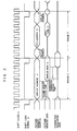
- a shift register 4 in Fig. 1 stores data to be displayed from a character generator 5 at the low level of a shift load signal a as shown in Fig. 2. Then, at the timing of a shift clock b, the data to be displayed is converted from parallel data into serial data, which is applied to a CRT display monitor 6 as a signal to be displayed thereon.
- the CRT controller 3 supplies a display address d corresponding to a position on the CRT at which data is to be displayed, through an address switching circuit 7 to the picture memory 2, and a data e to be displayed at the address d is applied to the ' character generator 5 as a code for a character to be displayed.
- the character generator 5 supplies a series of bits constituting a character corresponding to the character code to the shift register 4.
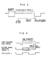
- a period F as shown in Fig. 2 when the CRT controller 3 is going to or operating to begin to read data from the picture memory 2, the CPU1 reads and writes the memory 2.
- the address switching circuit 7 changes to address a CPU address G from addressing of the display address d of the CRT controller 3 and supplies it to the picture memory 2.
- reading or writing of a CPU data H to the CPU address G by the CPU1 is carried out between the CPU1 and the picture memory 2 through a data buffer 10.
- a correct data e corresponding to the character to be displayed may not be obtained because in the period F the CPU1 reads or writes the picture memory 2 and accordingly a character which is different from the character to be displayed may be momentary displayed, and this may appear to be like a kind of noise.
- the following methods have been used conventionally:
- This invention is made for removing the above drawbacks in prior art, and this invention is featured in that in the period in which the CPU reads and writes the picture memory the switching signal for picture display is used as the CPU clock to the CPU1, and in the period in which the CPU neither reads nor writes the picture memory a CPU clock with a desired operating speed is applied to the CPU.
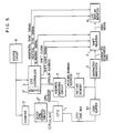
- Fig. 5 shows a block diagram of an embodiment of a display apparatus according to this invention
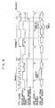
- Fig. 6 shows a timing chart to which reference is made in explaining the operation of the display apparatus as shown in Fig. 5.
- a CRT controller 3 a source oscillator 8, a counter 9, a picture memory 2, an address switching circuit 7, a CPU1, a data buffer 10, a character generator 5, a shift register 4, a CRT display monitor 6, a display clock signal generating circuit 3' belonging to the CRT controller 3, and a CPU clock synchronizing control circuit 3".
- an oscillation output signal generated from the source oscillator 8 is applied to the CRT controller 3 and counter 3', which then generate horizontal and vertical synchronizing signals to be supplied to the CRT display monitor 6, a blanking signal, shift clock, and shift load signal etc. to be applied to the shift register 4, and a display address to be applied to the picture memory 2.
- the display address generated from the CRT controller 3 is applied through the address switching circuit 7 to the picture memory 2 when the picture display switching signal O, as shown in Fig. 6, generated from the counter 3' is at low level during a period P.
- the picture memory 2 supplies a display data located at the display address to the character generator 5, which then supplies to the shift register 4 a character bit series corresponding to the applied display data.
- the shift register 4 latches the series of bits of the character at low level of a shift register load signal a as shown in Fig. 6 and then converts the bit series of the character into a serial data at the timing of a shift clock.
- the serial data is applied to the CRT display 6 as a video signal, so that the character appears on the display screen.
- the CPU1 in Fig. 5 When the CPU1 in Fig. 5 does not read or write the picture memory 2, it operates at high speed in response to a high-frequency CPU clock as shown in Fig. 6 by a period C. However, when the CPU1 is going to read or write the picture memory 2, a picture memory selecting signal Q to the picture memory 2 generated from a decoder (not shown) for decoding the CPU address is applied to the clock synchronizing control circuit 3" and the address switching circuit 7. Thereby, the CPU clock to the CPU1 is controlled by the clock synchronizing control circuit 3" to be synchro- . nized with the picture display switching signal O as shown in Fig. 6 by a period F.
- the CPU address from the CPU1 is applied through the address switching circuit 7 to the picture memory 2 when the picture display switching signal O from the counter 3' is at high level during a period R.
- a CPU data H is read from and is written in the location corresponding to the CPU address thus applied from the CPU1.
- the CPU1 After the CPU1 completes the read or write operation on the picture memory 2, the CPU1 operates in response to the high frequency CPU clock as shown in Fig. 6 by period C.
- the CPU1 when the CPU1 does not carry out any of reading or writing of the picture memory 2, the CPU1 can operate at high speed. Moreover, even when the CPU1 reads or writes the picture memory 2, the CPU1 is synchronized with the display timing, therefore, no flickers, noises or other interferences appear on the CRT display screen, and also since the CPU1 does not require unnecessary waiting time it is possible to read or write at high speed.
- Fig. 7 shows this specific example of the circuit arrangement. Referring to Fig. 7, there are shown the 1/16- frequency dividing counter 3' using, for example, 74 LS 161 and others, the 1/6-frequency dividing counter 9 using, for example, 74 LS 92, a NOR gate 31', an OR gate 31", an AND gate 32', an AND gate 33", an AND gate 34", a D type flip-flop 35", an OR gate 36", inverters 37" and 38", and an inverter 32'.
- an oscillation output signal S from the source oscillator 8 is applied to and divided in its frequency by the counters 3' and 9.
- a shift load signal a as shown in Fig. 8 is the output from the inverter 32' to which one (carry signal) of the frequency-divided output signals from the counter 3' is applied.
- the shift load signal a is used as a load signal to the parallel-to-serial converting shift register 4.
- a 1/8-frequency divided signal O D and a 1/4-frequency divided signal Q c are applied to the NOR gate 31', the output of which is used as the picture switching signal O.
- the AND gate 34 when supplied with low level from the true output (Q o ) of the flip-flop 35" or low level from the output of the NOR gate 31', produces low-level output, i.e., generates a switching inhibit signal W for CPU clock.
- the CPU1 reads or writes the picture memory 2
- the picture memory selecting signal Q as shown in Fig. 7 becomes low level.
- the gate 36 functions as an AND gate (negative logic) to produce low-level output, when the switching inhibit signal W and the picture memory selecting signal Q become low level.
- the flip-flop 35" latches the output from the gate 36" at the leading edges of the output of the counter 9.
- the flip-flop 35" controls the switching circuit consisting of the gates 31", 32" and 33" so that when the true output of the flip-flop 35" is high level, the output of the counter 9 is used as the CPU clock to the CPU1, and when the true output thereof is low level, the output of the NOR gate 31' is used as the CPU clock.
- the inverters 37" and 38" are used for delay.
- the CPU1 reads or writes the picture memory 2
- the picture memory selecting signal Q becomes low level (T i in Fig. 8).
- the flip-flop 35" for storing the clock switching control signal stores the output signal U from the gate 36" at the leading edge (T 2 ) of the output of the counter 9. In Fig. 8, at T 2 the output signal U is high level and thus no switching occurs.
- the output signal U from the gate 36" has become low level and thus the true output of the flip-flop 35" is low level, or the false output (Go) thereof is high level.
- the output of the gate 31' is selected for the CPU clock to the CPU1.
- the timing at which the CPU1 completes reading or writing of the picture memory 2 will be described with reference to Fig. 9.
- the flip-flop 35", at T 6 stores, the output signal U from the gate 36" and produces high level output at the true output.
- the gates 32", 33" and 34" are controlled to select the output signal from the counter 9 by switching the outputs of the gate 31' and counter 9 and as a result the gate 31" supplies the output of the counter 9 as the CPU clock to the CPU1.
- the CPU clock to the CPU1 results from division of the frequency of the oscillation output signal S by six when the picture memory 2 is not read or written, or from dividing it by 16 when the picture memory 2 is read or written.
- the CPU1 can be operated at a speed 2.66 times higher than in the case where the picture switching signal 0 is always selected as the CPU clock to the CPU1.
- the circuit constructed with the gates 31' and 34" may be constructed with the combination of logic gates, for example, AND, NOT, OR gates and the like for logically gating the output signals from the counter 3' and flip-flop 35" in Fig. 7, at which time the same effect as in the above mentioned embodiment can of course be achieved.
- the flip-flop 35" may be replaced by a device having a temporal storing function, such as an RS flip-flop, a J-K flip-flop, or a memory etc.
- the switching circuit formed of the gates 31", 32' and 33" may be replaced by another device having a switching function, such as a switch and a switching gate etc.
Landscapes
- Engineering & Computer Science (AREA)
- Physics & Mathematics (AREA)
- Computer Hardware Design (AREA)
- General Physics & Mathematics (AREA)
- Theoretical Computer Science (AREA)
- Radar, Positioning & Navigation (AREA)
- Remote Sensing (AREA)
- Multimedia (AREA)
- Controls And Circuits For Display Device (AREA)
- Digital Computer Display Output (AREA)
Claims (3)
Applications Claiming Priority (2)
| Application Number | Priority Date | Filing Date | Title |
|---|---|---|---|
| JP184283/80 | 1980-12-24 | ||
| JP55184283A JPS602669B2 (ja) | 1980-12-24 | 1980-12-24 | 画面表示装置 |
Publications (2)
| Publication Number | Publication Date |
|---|---|
| EP0054906A1 EP0054906A1 (de) | 1982-06-30 |
| EP0054906B1 true EP0054906B1 (de) | 1986-04-23 |
Family
ID=16150604
Family Applications (1)
| Application Number | Title | Priority Date | Filing Date |
|---|---|---|---|
| EP81110504A Expired EP0054906B1 (de) | 1980-12-24 | 1981-12-16 | Anzeigevorrichtung |
Country Status (4)
| Country | Link |
|---|---|
| US (1) | US4468662A (de) |
| EP (1) | EP0054906B1 (de) |
| JP (1) | JPS602669B2 (de) |
| DE (1) | DE3174492D1 (de) |
Families Citing this family (17)
| Publication number | Priority date | Publication date | Assignee | Title |
|---|---|---|---|---|
| DE3382253D1 (de) * | 1982-05-31 | 1991-05-23 | Fuji Xerox Co Ltd | Bilddatenspeichersystem. |
| JPS5960480A (ja) * | 1982-09-29 | 1984-04-06 | フアナツク株式会社 | デイスプレイ装置 |
| EP0112415B1 (de) * | 1982-12-22 | 1987-03-18 | International Business Machines Corporation | Verfahren und Vorrichtung zum kontinuierlichen Aktualisieren einer Koordinatenanzeige eines Lichtgriffels |
| JPS59159196A (ja) * | 1983-02-24 | 1984-09-08 | インタ−ナシヨナル ビジネス マシ−ンズ コ−ポレ−シヨン | グラフイツク・デイスプレイ・システム |
| JPS6067989A (ja) * | 1983-09-26 | 1985-04-18 | 株式会社日立製作所 | 画像表示装置 |
| JPS60113395A (ja) * | 1983-11-25 | 1985-06-19 | Hitachi Ltd | メモリ制御回路 |
| US4622546A (en) * | 1983-12-23 | 1986-11-11 | Advanced Micro Devices, Inc. | Apparatus and method for displaying characters in a bit mapped graphics system |
| JPS60225887A (ja) * | 1984-04-19 | 1985-11-11 | エヌ・シー・アール・コーポレーション | Crtデイスプレイ装置 |
| JPS6125184A (ja) * | 1984-07-13 | 1986-02-04 | 株式会社 アスキ− | 表示制御装置 |
| JPS61110198A (ja) * | 1984-11-05 | 1986-05-28 | 株式会社東芝 | マトリクス形表示装置 |
| JPS61159686A (ja) * | 1985-01-07 | 1986-07-19 | 株式会社日立製作所 | 画像表示装置 |
| US4679041A (en) * | 1985-06-13 | 1987-07-07 | Sun Microsystems, Inc. | High speed Z-buffer with dynamic random access memory |
| JP2520872B2 (ja) * | 1985-12-10 | 1996-07-31 | オリンパス光学工業株式会社 | 画像表示装置 |
| KR900005188B1 (ko) * | 1986-07-25 | 1990-07-20 | 후지쓰 가부시끼가이샤 | Crt 콘트롤러 |
| JPS63168684A (ja) * | 1986-12-29 | 1988-07-12 | ブラザー工業株式会社 | 表示装置 |
| US5757365A (en) * | 1995-06-07 | 1998-05-26 | Seiko Epson Corporation | Power down mode for computer system |
| US6088806A (en) * | 1998-10-20 | 2000-07-11 | Seiko Epson Corporation | Apparatus and method with improved power-down mode |
Family Cites Families (3)
| Publication number | Priority date | Publication date | Assignee | Title |
|---|---|---|---|---|
| US3803584A (en) * | 1971-02-16 | 1974-04-09 | Courier Terminal Syst Inc | Display system |
| US4298931A (en) * | 1978-06-02 | 1981-11-03 | Hitachi, Ltd. | Character pattern display system |
| JPS6036592B2 (ja) * | 1979-06-13 | 1985-08-21 | 株式会社日立製作所 | 文字図形表示装置 |
-
1980
- 1980-12-24 JP JP55184283A patent/JPS602669B2/ja not_active Expired
-
1981
- 1981-12-16 EP EP81110504A patent/EP0054906B1/de not_active Expired
- 1981-12-16 DE DE8181110504T patent/DE3174492D1/de not_active Expired
- 1981-12-17 US US06/331,871 patent/US4468662A/en not_active Expired - Fee Related
Also Published As
| Publication number | Publication date |
|---|---|
| US4468662A (en) | 1984-08-28 |
| DE3174492D1 (en) | 1986-05-28 |
| JPS57105781A (en) | 1982-07-01 |
| EP0054906A1 (de) | 1982-06-30 |
| JPS602669B2 (ja) | 1985-01-23 |
Similar Documents
| Publication | Publication Date | Title |
|---|---|---|
| EP0054906B1 (de) | Anzeigevorrichtung | |
| US4204206A (en) | Video display system | |
| US5610622A (en) | Display control device | |
| US4485378A (en) | Display control apparatus | |
| JPH10153989A (ja) | ドットクロック回路 | |
| KR920000455B1 (ko) | 인터페이스 장치 | |
| EP0019366B1 (de) | Vorrichtung zur Steuerung der Darstellung von Cursoren bei einem Anzeigesystem mit Raster-Abtastung | |
| EP0366124A1 (de) | Halbbild-Diskriminierschaltung | |
| EP0120142B1 (de) | Graphisches Anzeigesystem | |
| JPS642955B2 (de) | ||
| EP0140555A2 (de) | Gerät zur Anzeige von durch eine Vielheit von Datenzeilen definierten Bildern | |
| US4581611A (en) | Character display system | |
| JPS6249630B2 (de) | ||
| US4876533A (en) | Method and apparatus for removing an image from a window of a display | |
| US5339160A (en) | Character display device for synchronizing operation of video ram to operation of CPU | |
| JPH0136146B2 (de) | ||
| US5055940A (en) | Video memory control apparatus | |
| US4546350A (en) | Display apparatus | |
| US4965563A (en) | Flat display driving circuit for a display containing margins | |
| US3544712A (en) | Multiplexed digital flyback control of crt displays | |
| SU1469518A1 (ru) | Устройство дл отображени информации на экране телевизионного индикатора | |
| JPH087547B2 (ja) | 表示メモリアドレス装置 | |
| EP0470768B1 (de) | Planung von Zeichenoperationen von beweglichen Bildern | |
| JPS6129885A (ja) | 表示メモリのアクセス信号発生装置 | |
| SU1656520A2 (ru) | Устройство дл отображени информации на экране телевизионного индикатора |
Legal Events
| Date | Code | Title | Description |
|---|---|---|---|
| PUAI | Public reference made under article 153(3) epc to a published international application that has entered the european phase |
Free format text: ORIGINAL CODE: 0009012 |
|
| AK | Designated contracting states |
Designated state(s): DE FR GB IT |
|
| 17P | Request for examination filed |
Effective date: 19821229 |
|
| GRAA | (expected) grant |
Free format text: ORIGINAL CODE: 0009210 |
|
| AK | Designated contracting states |
Kind code of ref document: B1 Designated state(s): DE FR GB IT |
|
| ITF | It: translation for a ep patent filed | ||
| REF | Corresponds to: |
Ref document number: 3174492 Country of ref document: DE Date of ref document: 19860528 |
|
| ET | Fr: translation filed | ||
| PLBE | No opposition filed within time limit |
Free format text: ORIGINAL CODE: 0009261 |
|
| STAA | Information on the status of an ep patent application or granted ep patent |
Free format text: STATUS: NO OPPOSITION FILED WITHIN TIME LIMIT |
|
| 26N | No opposition filed | ||
| ITTA | It: last paid annual fee | ||
| PGFP | Annual fee paid to national office [announced via postgrant information from national office to epo] |
Ref country code: GB Payment date: 19941206 Year of fee payment: 14 |
|
| PGFP | Annual fee paid to national office [announced via postgrant information from national office to epo] |
Ref country code: DE Payment date: 19941208 Year of fee payment: 14 |
|
| PGFP | Annual fee paid to national office [announced via postgrant information from national office to epo] |
Ref country code: FR Payment date: 19941209 Year of fee payment: 14 |
|
| PG25 | Lapsed in a contracting state [announced via postgrant information from national office to epo] |
Ref country code: GB Effective date: 19951216 |
|
| GBPC | Gb: european patent ceased through non-payment of renewal fee |
Effective date: 19951216 |
|
| PG25 | Lapsed in a contracting state [announced via postgrant information from national office to epo] |
Ref country code: FR Effective date: 19960830 |
|
| PG25 | Lapsed in a contracting state [announced via postgrant information from national office to epo] |
Ref country code: DE Effective date: 19960903 |
|
| REG | Reference to a national code |
Ref country code: FR Ref legal event code: ST |