EP0012863B1 - Procédé de fabrication de dispositifs semi-conducteurs à capacitance parasitaire réduite - Google Patents
Procédé de fabrication de dispositifs semi-conducteurs à capacitance parasitaire réduite Download PDFInfo
- Publication number
- EP0012863B1 EP0012863B1 EP79104724A EP79104724A EP0012863B1 EP 0012863 B1 EP0012863 B1 EP 0012863B1 EP 79104724 A EP79104724 A EP 79104724A EP 79104724 A EP79104724 A EP 79104724A EP 0012863 B1 EP0012863 B1 EP 0012863B1
- Authority
- EP
- European Patent Office
- Prior art keywords
- layer
- region
- conductive layer
- substrate
- doping region
- Prior art date
- Legal status (The legal status is an assumption and is not a legal conclusion. Google has not performed a legal analysis and makes no representation as to the accuracy of the status listed.)
- Expired
Links
- 239000004065 semiconductor Substances 0.000 title claims description 15
- 238000004519 manufacturing process Methods 0.000 title claims description 9
- 230000002829 reductive effect Effects 0.000 title claims description 9
- 230000003071 parasitic effect Effects 0.000 title description 6
- 238000000034 method Methods 0.000 claims description 51
- 239000000758 substrate Substances 0.000 claims description 31
- 230000000873 masking effect Effects 0.000 claims description 23
- 229910021420 polycrystalline silicon Inorganic materials 0.000 claims description 20
- 230000008569 process Effects 0.000 claims description 16
- 238000005530 etching Methods 0.000 claims description 15
- 230000008878 coupling Effects 0.000 claims description 11
- 238000010168 coupling process Methods 0.000 claims description 11
- 238000005859 coupling reaction Methods 0.000 claims description 11
- 238000003860 storage Methods 0.000 claims description 8
- 238000001020 plasma etching Methods 0.000 claims description 2
- 229920000642 polymer Polymers 0.000 claims description 2
- 229920000620 organic polymer Polymers 0.000 claims 1
- 239000000126 substance Substances 0.000 claims 1
- 229920002120 photoresistant polymer Polymers 0.000 description 25
- KRHYYFGTRYWZRS-UHFFFAOYSA-N Fluorane Chemical compound F KRHYYFGTRYWZRS-UHFFFAOYSA-N 0.000 description 8
- VYPSYNLAJGMNEJ-UHFFFAOYSA-N Silicium dioxide Chemical compound O=[Si]=O VYPSYNLAJGMNEJ-UHFFFAOYSA-N 0.000 description 8
- 239000003990 capacitor Substances 0.000 description 5
- QVGXLLKOCUKJST-UHFFFAOYSA-N atomic oxygen Chemical compound [O] QVGXLLKOCUKJST-UHFFFAOYSA-N 0.000 description 4
- 238000011161 development Methods 0.000 description 4
- 238000009792 diffusion process Methods 0.000 description 4
- 230000001788 irregular Effects 0.000 description 4
- 239000001301 oxygen Substances 0.000 description 4
- 229910052760 oxygen Inorganic materials 0.000 description 4
- 235000012239 silicon dioxide Nutrition 0.000 description 4
- 239000000377 silicon dioxide Substances 0.000 description 4
- VEXZGXHMUGYJMC-UHFFFAOYSA-N Hydrochloric acid Chemical compound Cl VEXZGXHMUGYJMC-UHFFFAOYSA-N 0.000 description 3
- BLRPTPMANUNPDV-UHFFFAOYSA-N Silane Chemical compound [SiH4] BLRPTPMANUNPDV-UHFFFAOYSA-N 0.000 description 3
- 238000004140 cleaning Methods 0.000 description 3
- 229910000041 hydrogen chloride Inorganic materials 0.000 description 3
- IXCSERBJSXMMFS-UHFFFAOYSA-N hydrogen chloride Substances Cl.Cl IXCSERBJSXMMFS-UHFFFAOYSA-N 0.000 description 3
- 238000009413 insulation Methods 0.000 description 3
- 238000002955 isolation Methods 0.000 description 3
- 239000000463 material Substances 0.000 description 3
- 230000003647 oxidation Effects 0.000 description 3
- 238000007254 oxidation reaction Methods 0.000 description 3
- 229910000077 silane Inorganic materials 0.000 description 3
- DDFHBQSCUXNBSA-UHFFFAOYSA-N 5-(5-carboxythiophen-2-yl)thiophene-2-carboxylic acid Chemical compound S1C(C(=O)O)=CC=C1C1=CC=C(C(O)=O)S1 DDFHBQSCUXNBSA-UHFFFAOYSA-N 0.000 description 2
- QGZKDVFQNNGYKY-UHFFFAOYSA-N Ammonia Chemical compound N QGZKDVFQNNGYKY-UHFFFAOYSA-N 0.000 description 2
- IJGRMHOSHXDMSA-UHFFFAOYSA-N Atomic nitrogen Chemical compound N#N IJGRMHOSHXDMSA-UHFFFAOYSA-N 0.000 description 2
- NBIIXXVUZAFLBC-UHFFFAOYSA-N Phosphoric acid Chemical compound OP(O)(O)=O NBIIXXVUZAFLBC-UHFFFAOYSA-N 0.000 description 2
- 229910052581 Si3N4 Inorganic materials 0.000 description 2
- 238000010276 construction Methods 0.000 description 2
- 238000013461 design Methods 0.000 description 2
- 230000000694 effects Effects 0.000 description 2
- 239000007789 gas Substances 0.000 description 2
- 238000012856 packing Methods 0.000 description 2
- 238000000206 photolithography Methods 0.000 description 2
- 230000009467 reduction Effects 0.000 description 2
- 230000000717 retained effect Effects 0.000 description 2
- HQVNEWCFYHHQES-UHFFFAOYSA-N silicon nitride Chemical compound N12[Si]34N5[Si]62N3[Si]51N64 HQVNEWCFYHHQES-UHFFFAOYSA-N 0.000 description 2
- XLYOFNOQVPJJNP-UHFFFAOYSA-N water Chemical compound O XLYOFNOQVPJJNP-UHFFFAOYSA-N 0.000 description 2
- ZNQVEEAIQZEUHB-UHFFFAOYSA-N 2-ethoxyethanol Chemical compound CCOCCO ZNQVEEAIQZEUHB-UHFFFAOYSA-N 0.000 description 1
- ZRUOTKQBVMWMDK-UHFFFAOYSA-N 2-hydroxy-6-methylbenzaldehyde Chemical compound CC1=CC=CC(O)=C1C=O ZRUOTKQBVMWMDK-UHFFFAOYSA-N 0.000 description 1
- ZOXJGFHDIHLPTG-UHFFFAOYSA-N Boron Chemical compound [B] ZOXJGFHDIHLPTG-UHFFFAOYSA-N 0.000 description 1
- SECXISVLQFMRJM-UHFFFAOYSA-N N-Methylpyrrolidone Chemical compound CN1CCCC1=O SECXISVLQFMRJM-UHFFFAOYSA-N 0.000 description 1
- GRYLNZFGIOXLOG-UHFFFAOYSA-N Nitric acid Chemical compound O[N+]([O-])=O GRYLNZFGIOXLOG-UHFFFAOYSA-N 0.000 description 1
- XUIMIQQOPSSXEZ-UHFFFAOYSA-N Silicon Chemical compound [Si] XUIMIQQOPSSXEZ-UHFFFAOYSA-N 0.000 description 1
- 239000002253 acid Substances 0.000 description 1
- 239000000654 additive Substances 0.000 description 1
- 230000000996 additive effect Effects 0.000 description 1
- JRBRVDCKNXZZGH-UHFFFAOYSA-N alumane;copper Chemical compound [AlH3].[Cu] JRBRVDCKNXZZGH-UHFFFAOYSA-N 0.000 description 1
- XAGFODPZIPBFFR-UHFFFAOYSA-N aluminium Chemical compound [Al] XAGFODPZIPBFFR-UHFFFAOYSA-N 0.000 description 1
- 229910052782 aluminium Inorganic materials 0.000 description 1
- 238000000637 aluminium metallisation Methods 0.000 description 1
- 229910000147 aluminium phosphate Inorganic materials 0.000 description 1
- 229910021529 ammonia Inorganic materials 0.000 description 1
- RBFQJDQYXXHULB-UHFFFAOYSA-N arsane Chemical compound [AsH3] RBFQJDQYXXHULB-UHFFFAOYSA-N 0.000 description 1
- 229910052785 arsenic Inorganic materials 0.000 description 1
- RQNWIZPPADIBDY-UHFFFAOYSA-N arsenic atom Chemical compound [As] RQNWIZPPADIBDY-UHFFFAOYSA-N 0.000 description 1
- 125000004429 atom Chemical group 0.000 description 1
- 230000005540 biological transmission Effects 0.000 description 1
- 229910052796 boron Inorganic materials 0.000 description 1
- 238000009388 chemical precipitation Methods 0.000 description 1
- 239000004020 conductor Substances 0.000 description 1
- 239000000356 contaminant Substances 0.000 description 1
- 238000007796 conventional method Methods 0.000 description 1
- 239000013078 crystal Substances 0.000 description 1
- 238000000354 decomposition reaction Methods 0.000 description 1
- 230000007547 defect Effects 0.000 description 1
- 239000008367 deionised water Substances 0.000 description 1
- 229910021641 deionized water Inorganic materials 0.000 description 1
- 230000001419 dependent effect Effects 0.000 description 1
- XXTZHYXQVWRADW-UHFFFAOYSA-N diazomethanone Chemical compound [N]N=C=O XXTZHYXQVWRADW-UHFFFAOYSA-N 0.000 description 1
- 230000005669 field effect Effects 0.000 description 1
- 238000005247 gettering Methods 0.000 description 1
- 238000010438 heat treatment Methods 0.000 description 1
- 239000001257 hydrogen Substances 0.000 description 1
- 229910052739 hydrogen Inorganic materials 0.000 description 1
- 125000004435 hydrogen atom Chemical class [H]* 0.000 description 1
- 238000007689 inspection Methods 0.000 description 1
- 230000003993 interaction Effects 0.000 description 1
- 238000005468 ion implantation Methods 0.000 description 1
- 239000004922 lacquer Substances 0.000 description 1
- 230000007935 neutral effect Effects 0.000 description 1
- 229910017604 nitric acid Inorganic materials 0.000 description 1
- 229910052757 nitrogen Inorganic materials 0.000 description 1
- 229920003986 novolac Polymers 0.000 description 1
- 230000001590 oxidative effect Effects 0.000 description 1
- 238000002161 passivation Methods 0.000 description 1
- 239000012286 potassium permanganate Substances 0.000 description 1
- 238000001556 precipitation Methods 0.000 description 1
- 230000001681 protective effect Effects 0.000 description 1
- 229920005989 resin Polymers 0.000 description 1
- 239000011347 resin Substances 0.000 description 1
- 230000002441 reversible effect Effects 0.000 description 1
- 230000035945 sensitivity Effects 0.000 description 1
- 229910052710 silicon Inorganic materials 0.000 description 1
- 239000010703 silicon Substances 0.000 description 1
- XUIMIQQOPSSXEZ-IGMARMGPSA-N silicon-28 atom Chemical compound [28Si] XUIMIQQOPSSXEZ-IGMARMGPSA-N 0.000 description 1
- 239000002904 solvent Substances 0.000 description 1
- 238000004544 sputter deposition Methods 0.000 description 1
- 238000012956 testing procedure Methods 0.000 description 1
- 238000012546 transfer Methods 0.000 description 1
- 230000007704 transition Effects 0.000 description 1
- 238000005406 washing Methods 0.000 description 1
- 238000001039 wet etching Methods 0.000 description 1
Images

Classifications
-
- H—ELECTRICITY
- H01—ELECTRIC ELEMENTS
- H01L—SEMICONDUCTOR DEVICES NOT COVERED BY CLASS H10
- H01L21/00—Processes or apparatus adapted for the manufacture or treatment of semiconductor or solid state devices or of parts thereof
- H01L21/02—Manufacture or treatment of semiconductor devices or of parts thereof
- H01L21/04—Manufacture or treatment of semiconductor devices or of parts thereof the devices having potential barriers, e.g. a PN junction, depletion layer or carrier concentration layer
- H01L21/18—Manufacture or treatment of semiconductor devices or of parts thereof the devices having potential barriers, e.g. a PN junction, depletion layer or carrier concentration layer the devices having semiconductor bodies comprising elements of Group IV of the Periodic Table or AIIIBV compounds with or without impurities, e.g. doping materials
- H01L21/30—Treatment of semiconductor bodies using processes or apparatus not provided for in groups H01L21/20 - H01L21/26
- H01L21/31—Treatment of semiconductor bodies using processes or apparatus not provided for in groups H01L21/20 - H01L21/26 to form insulating layers thereon, e.g. for masking or by using photolithographic techniques; After treatment of these layers; Selection of materials for these layers
- H01L21/3105—After-treatment
- H01L21/31051—Planarisation of the insulating layers
- H01L21/31053—Planarisation of the insulating layers involving a dielectric removal step
- H01L21/31055—Planarisation of the insulating layers involving a dielectric removal step the removal being a chemical etching step, e.g. dry etching
-
- H—ELECTRICITY
- H01—ELECTRIC ELEMENTS
- H01L—SEMICONDUCTOR DEVICES NOT COVERED BY CLASS H10
- H01L21/00—Processes or apparatus adapted for the manufacture or treatment of semiconductor or solid state devices or of parts thereof
- H01L21/02—Manufacture or treatment of semiconductor devices or of parts thereof
- H01L21/04—Manufacture or treatment of semiconductor devices or of parts thereof the devices having potential barriers, e.g. a PN junction, depletion layer or carrier concentration layer
- H01L21/18—Manufacture or treatment of semiconductor devices or of parts thereof the devices having potential barriers, e.g. a PN junction, depletion layer or carrier concentration layer the devices having semiconductor bodies comprising elements of Group IV of the Periodic Table or AIIIBV compounds with or without impurities, e.g. doping materials
- H01L21/30—Treatment of semiconductor bodies using processes or apparatus not provided for in groups H01L21/20 - H01L21/26
- H01L21/31—Treatment of semiconductor bodies using processes or apparatus not provided for in groups H01L21/20 - H01L21/26 to form insulating layers thereon, e.g. for masking or by using photolithographic techniques; After treatment of these layers; Selection of materials for these layers
- H01L21/3205—Deposition of non-insulating-, e.g. conductive- or resistive-, layers on insulating layers; After-treatment of these layers
- H01L21/321—After treatment
- H01L21/3213—Physical or chemical etching of the layers, e.g. to produce a patterned layer from a pre-deposited extensive layer
- H01L21/32133—Physical or chemical etching of the layers, e.g. to produce a patterned layer from a pre-deposited extensive layer by chemical means only
- H01L21/32134—Physical or chemical etching of the layers, e.g. to produce a patterned layer from a pre-deposited extensive layer by chemical means only by liquid etching only
-
- H—ELECTRICITY
- H01—ELECTRIC ELEMENTS
- H01L—SEMICONDUCTOR DEVICES NOT COVERED BY CLASS H10
- H01L21/00—Processes or apparatus adapted for the manufacture or treatment of semiconductor or solid state devices or of parts thereof
- H01L21/70—Manufacture or treatment of devices consisting of a plurality of solid state components formed in or on a common substrate or of parts thereof; Manufacture of integrated circuit devices or of parts thereof
- H01L21/71—Manufacture of specific parts of devices defined in group H01L21/70
- H01L21/768—Applying interconnections to be used for carrying current between separate components within a device comprising conductors and dielectrics
- H01L21/76801—Applying interconnections to be used for carrying current between separate components within a device comprising conductors and dielectrics characterised by the formation and the after-treatment of the dielectrics, e.g. smoothing
- H01L21/76829—Applying interconnections to be used for carrying current between separate components within a device comprising conductors and dielectrics characterised by the formation and the after-treatment of the dielectrics, e.g. smoothing characterised by the formation of thin functional dielectric layers, e.g. dielectric etch-stop, barrier, capping or liner layers
- H01L21/76832—Multiple layers
-
- H—ELECTRICITY
- H01—ELECTRIC ELEMENTS
- H01L—SEMICONDUCTOR DEVICES NOT COVERED BY CLASS H10
- H01L23/00—Details of semiconductor or other solid state devices
- H01L23/52—Arrangements for conducting electric current within the device in operation from one component to another, i.e. interconnections, e.g. wires, lead frames
- H01L23/522—Arrangements for conducting electric current within the device in operation from one component to another, i.e. interconnections, e.g. wires, lead frames including external interconnections consisting of a multilayer structure of conductive and insulating layers inseparably formed on the semiconductor body
- H01L23/5222—Capacitive arrangements or effects of, or between wiring layers
-
- H—ELECTRICITY
- H10—SEMICONDUCTOR DEVICES; ELECTRIC SOLID-STATE DEVICES NOT OTHERWISE PROVIDED FOR
- H10B—ELECTRONIC MEMORY DEVICES
- H10B12/00—Dynamic random access memory [DRAM] devices
- H10B12/30—DRAM devices comprising one-transistor - one-capacitor [1T-1C] memory cells
-
- H—ELECTRICITY
- H01—ELECTRIC ELEMENTS
- H01L—SEMICONDUCTOR DEVICES NOT COVERED BY CLASS H10
- H01L2924/00—Indexing scheme for arrangements or methods for connecting or disconnecting semiconductor or solid-state bodies as covered by H01L24/00
- H01L2924/0001—Technical content checked by a classifier
- H01L2924/0002—Not covered by any one of groups H01L24/00, H01L24/00 and H01L2224/00
-
- Y—GENERAL TAGGING OF NEW TECHNOLOGICAL DEVELOPMENTS; GENERAL TAGGING OF CROSS-SECTIONAL TECHNOLOGIES SPANNING OVER SEVERAL SECTIONS OF THE IPC; TECHNICAL SUBJECTS COVERED BY FORMER USPC CROSS-REFERENCE ART COLLECTIONS [XRACs] AND DIGESTS
- Y10—TECHNICAL SUBJECTS COVERED BY FORMER USPC
- Y10S—TECHNICAL SUBJECTS COVERED BY FORMER USPC CROSS-REFERENCE ART COLLECTIONS [XRACs] AND DIGESTS
- Y10S438/00—Semiconductor device manufacturing: process
- Y10S438/901—Capacitive junction
Definitions
- the invention relates to a method for producing semiconductor arrangements with reduced capacitive coupling between at least one doping region arranged in a semiconductor substrate and an electrically conductive layer provided on the substrate in isolation, which is above the doping region a greater distance from the substrate surface than outside the doping region and thus is uneven Has surface with at least one raised area.
- it relates to measures for reducing parasitic bit line capacitances in memory arrangements in which the bit lines are designed in the form of doping regions in the semiconductor substrate in question, at least one electrically conductive layer being provided over the substrate.
- US patent specification 3976524 a method for producing flat surfaces in integrated circuits, in which the surface to be leveled is first coated with a photoresist layer, which forms a photoresist pattern in the recessed areas after appropriate exposure and development in the raised areas from these and from the recessed areas marginally exposed and developed areas is removed. The unexposed photoresist pattern is then melted so that the recessed areas are completely masked. The raised areas can then be removed to the depth of the recessed areas.
- US Pat. No. 4,070,501 is also of interest, which relates to a method for the self-aligning production of multilayer pipe systems with cross connections.
- an insulation layer is applied to a substrate carrying a first line pattern, which corresponds to the surface of the topology of the line pattern, that is to say has corresponding elevations.
- a second layer is applied to the insulation layer, the thickness of which is less above the cable runs than next to them.
- the material of the second layer above the elevations is removed by means of a mask in the area of the connection holes to be formed above the cable runs.
- the connection holes in the insulation layer are formed by etching, the mask and the second layer serving as an etching mask.
- the invention achieves the object of specifying an improved production method for semiconductor arrangements with reduced parasitic capacitances, which can result from the interaction of doping regions in a substrate with conductive layers or layer regions arranged above them.
- the method should make it possible to produce capacitive single-FET memory arrangements with reduced bit line capacitance.
- the invention provides for reducing the capacitive coupling between at least one doping region arranged in a semiconductor substrate and an electrically conductive layer provided on the substrate in isolation, which is above the doping region a greater distance from the substrate surface than outside the doping region and thus an uneven surface with at least one has raised area, before to apply a relatively thick masking layer, preferably made of photoresist, to the surface of the conductive layer such that the conductive layer is completely covered with an irregular surface and a practically flat surface is formed. Then a subtractive process, e.g. an etching or development process is carried out in order to remove a uniform layer portion of the masking layer to such an extent that the raised areas of the surface of the conductive layer are exposed in some areas.
- a subtractive process e.g. an etching or development process
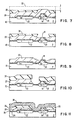
- FIG. 1 shows a semiconductor substrate 10, which is preferably made of P-conducting silicon with a specific resistance of approximately 2 to 12 ⁇ . cm.
- a layer of an arsenic-doped oxide, designated 12 is applied to the substrate 10.
- the substrate 10 was introduced into an atmosphere of gaseous silane, arsine, oxygen and nitrogen in suitable amounts for chemical precipitation by decomposition from the gas phase (CVD) in such a way that a doped oxide layer 12 of approximately 300 to 500 nm is formed, which as Diffusion source layer can serve to form PN junctions in the substrate.
- This CVD process is best carried out at around 500 ° C in an apparatus such as that e.g. in U.S. Patent 3,805,736.
- a photolithographic masking step is carried out in order to define all the regions on the surface of the substrate 10 in which diffused transitions are desired.
- the doped oxide layer 12 is then (selectively) removed in a wet etching process, for example in hydrofluoric acid buffered with ammonium fluoride.
- the regions of the doped oxide layer denoted by 14 and 16 remain on the surface of the substrate 10 in the manner shown in FIG. 2. Although a very large number of such doped regions is normally provided, only two such regions are shown in this case to describe the invention.
- the designated area 14 is in reality an extended strip which extends perpendicular to the plane and a bit - represents sense line.
- the area designated 16 is one of many areas arranged adjacent to area 14, each of which forms an isolated capacitance area.
- an uncritical (not shown) rough masking is applied, which is designed in such a way that the doped oxide layer regions can be selectively removed over such doping regions, to which a capacitively coupled covering layer of conductive material must be applied.
- a brief dip etch is performed to remove any remnant of the thermal oxide layer 18 that was previously present under the coarse masking and adjacent to the remaining oxide layer area 14, see FIG. in this respect also US Pat. No. 3,975,220.
- FIG. 4 illustrates the result following this method step.
- the oxide region denoted by 14 is maintained above the associated doping region 20 for the (diffused) bit sensing line.
- a thin thermal silicon dioxide layer 24 of about 30 nm thickness is washed in an atmosphere containing oxygen / hydrogen chloride at about 1000 ° C.
- This layer, designated 24, covers the entire exposed surface with the exception of the locations where doped oxide is present.
- This method step can also be carried out in a device of the type described in more detail in US Pat. No. 3,790,404.
- an approximately 20 nm thick silicon nitride layer 26 is applied using an atmosphere containing silane and ammonia at approximately 900 ° C.
- This is followed by the precipitation of an approximately 300 nm thick polycrystalline silicon layer 28 doped with boron from an atmosphere containing hydrogen, silane and borohydride at approximately 600 ° C.
- the latter two process steps can be carried out successively in a common process chamber of the type described in more detail in US Pat. No. 3,805,763.
- the polycrystalline silicon layer 28 is retained in some areas, namely over the doping regions 22 for the storage nodes, where it represents an electrode of the storage capacitor of the relevant memory cell, or as a shielding layer over the substrate around the doping regions 22. Layer 28 also remained over the entire length of the bit sense lines doping regions 20, which made a significant amount to increase the effective coupling capacity. This effect occurred regardless of the effective reduction in capacitive effects achieved by maintaining both the distance between the capacitor electrodes and between the doping regions 20 and the conductive layer 28 by maintaining the doped oxide regions 14.
- a relatively thick photoresist masking layer 30 is applied to the substrate.
- the layer 30 is so thick that it covers all areas of the layer designated 28 and forms an essentially flat surface according to FIG. 6.
- a conventional positive lacquer which is sold under the trade name AZ1350J by the Shipley Company, Newton, Massachusetts, can be used as the photoresist for the layer 30.
- AZ1350J is a light-sensitive polymer consisting of an m-cresol-formaldehyde novolak resin and a diazo-ketone sensitizer, dissolved in ethylene-glycol-monoethyl ether acetate.
- the photoresist may contain an additive to improve the adhesion properties, e.g.
- the photoresist can be applied using one of the conventional techniques that allow the application of so much material that an essentially flat surface can be obtained.
- the photoresist is then treated by heat treatment at 95 ° C for a time sufficient for curing.
- Consistent uniform exposure of the photoresist through a neutral density filter in order to reduce the development rate sufficiently to control the development depth L cf. e.g. U.S. Patent 3649393.
- removal by means of reactive ion etching or by means of a sputtering process can also be considered. Since a uniform photoresist layer is removed, this process step is self-adjusting and selectively exposes only the areas of the coated substrate that extend through the remaining photoresist masking layer in the manner shown in FIG.
- the then exposed polycrystalline silicon is selectively removed using a suitable etchant, e.g. by means of a solution of nitric acid, water and buffered hydrofluoric acid in a volume ratio of 7: 4: 1, the buffered hydrofluoric acid having 5 parts by volume of 40% ammonium fluoride per part by volume of 48% hydrofluoric acid.
- a suitable etchant e.g. by means of a solution of nitric acid, water and buffered hydrofluoric acid in a volume ratio of 7: 4: 1, the buffered hydrofluoric acid having 5 parts by volume of 40% ammonium fluoride per part by volume of 48% hydrofluoric acid.
- the further procedure can be carried out in the following manner in accordance with US Pat. No. 3,841,926.
- a further photolithography and etching step is used to etch the regions of the polycrystalline silicon layer 28 at which gate regions are required for the respective field effect transistors, cf. Fig. 10.
- this etching step is, however, limited to relatively small gates. Areas are limited, thereby coupling each of the numerous isolated areas 22 of the storage nodes to the elongated doping region 20 of the associated bit line.
- the actual memory cells which consist of the doping regions 20 for the bit sensing lines, the gate electrodes 38, and the storage nodes 22 and Capacitor electrodes (regions of the layer 28 above the doping regions 22) exist, are fully functional and testable.
- the electrical isolation of adjacent storage nodes 22 is possible by applying a reference potential to the polycrystalline silicon layer 28 so that the surface of the substrate 10 adjacent to the regions 20 and 22, but not under the electrodes 38 between these regions, is continuously reverse biased . This can be accomplished by applying substrate 10 and polycrystalline silicon layer 28 to a negative voltage.
Landscapes
- Engineering & Computer Science (AREA)
- Physics & Mathematics (AREA)
- Condensed Matter Physics & Semiconductors (AREA)
- General Physics & Mathematics (AREA)
- Computer Hardware Design (AREA)
- Microelectronics & Electronic Packaging (AREA)
- Power Engineering (AREA)
- Manufacturing & Machinery (AREA)
- Chemical & Material Sciences (AREA)
- Chemical Kinetics & Catalysis (AREA)
- General Chemical & Material Sciences (AREA)
- Semiconductor Memories (AREA)
- Local Oxidation Of Silicon (AREA)
- Static Random-Access Memory (AREA)
- Internal Circuitry In Semiconductor Integrated Circuit Devices (AREA)
- Semiconductor Integrated Circuits (AREA)
Claims (7)
Applications Claiming Priority (2)
| Application Number | Priority Date | Filing Date | Title |
|---|---|---|---|
| US05/973,219 US4222816A (en) | 1978-12-26 | 1978-12-26 | Method for reducing parasitic capacitance in integrated circuit structures |
| US973219 | 2001-10-09 |
Publications (3)
| Publication Number | Publication Date |
|---|---|
| EP0012863A2 EP0012863A2 (fr) | 1980-07-09 |
| EP0012863A3 EP0012863A3 (en) | 1980-10-15 |
| EP0012863B1 true EP0012863B1 (fr) | 1982-07-28 |
Family
ID=25520641
Family Applications (1)
| Application Number | Title | Priority Date | Filing Date |
|---|---|---|---|
| EP79104724A Expired EP0012863B1 (fr) | 1978-12-26 | 1979-11-27 | Procédé de fabrication de dispositifs semi-conducteurs à capacitance parasitaire réduite |
Country Status (4)
| Country | Link |
|---|---|
| US (1) | US4222816A (fr) |
| EP (1) | EP0012863B1 (fr) |
| JP (1) | JPS5591158A (fr) |
| DE (1) | DE2963453D1 (fr) |
Families Citing this family (13)
| Publication number | Priority date | Publication date | Assignee | Title |
|---|---|---|---|---|
| US4295924A (en) * | 1979-12-17 | 1981-10-20 | International Business Machines Corporation | Method for providing self-aligned conductor in a V-groove device |
| JPS5793572A (en) * | 1980-12-03 | 1982-06-10 | Nec Corp | Manufacture of semiconductor device |
| JPS59161069A (ja) * | 1983-03-04 | 1984-09-11 | Oki Electric Ind Co Ltd | Mos型半導体装置の製造方法 |
| JPS6045057A (ja) * | 1983-08-23 | 1985-03-11 | Toshiba Corp | 固体撮像装置の製造方法 |
| US4478679A (en) * | 1983-11-30 | 1984-10-23 | Storage Technology Partners | Self-aligning process for placing a barrier metal over the source and drain regions of MOS semiconductors |
| US4594769A (en) * | 1984-06-15 | 1986-06-17 | Signetics Corporation | Method of forming insulator of selectively varying thickness on patterned conductive layer |
| US5734188A (en) * | 1987-09-19 | 1998-03-31 | Hitachi, Ltd. | Semiconductor integrated circuit, method of fabricating the same and apparatus for fabricating the same |
| DE68923301D1 (de) * | 1988-02-17 | 1995-08-10 | Fujitsu Ltd | Halbleiteranordnung mit einer dünnen isolierenden Schicht. |
| US5214304A (en) * | 1988-02-17 | 1993-05-25 | Fujitsu Limited | Semiconductor device |
| US5917211A (en) * | 1988-09-19 | 1999-06-29 | Hitachi, Ltd. | Semiconductor integrated circuit, method of fabricating the same and apparatus for fabricating the same |
| US5589423A (en) * | 1994-10-03 | 1996-12-31 | Motorola Inc. | Process for fabricating a non-silicided region in an integrated circuit |
| US6342681B1 (en) * | 1997-10-15 | 2002-01-29 | Avx Corporation | Surface mount coupler device |
| DE19753782A1 (de) * | 1997-12-04 | 1999-06-10 | Inst Halbleiterphysik Gmbh | Verfahren zur Planarisierung von Silizium-Wafern |
Family Cites Families (9)
| Publication number | Priority date | Publication date | Assignee | Title |
|---|---|---|---|---|
| CH573661A5 (fr) * | 1973-01-02 | 1976-03-15 | Ibm | |
| US3841926A (en) * | 1973-01-02 | 1974-10-15 | Ibm | Integrated circuit fabrication process |
| US3976524A (en) * | 1974-06-17 | 1976-08-24 | Ibm Corporation | Planarization of integrated circuit surfaces through selective photoresist masking |
| DE2547792C3 (de) * | 1974-10-25 | 1978-08-31 | Hitachi, Ltd., Tokio | Verfahren zur Herstellung eines Halbleiterbauelementes |
| US3975220A (en) * | 1975-09-05 | 1976-08-17 | International Business Machines Corporation | Diffusion control for controlling parasitic capacitor effects in single FET structure arrays |
| US4045594A (en) * | 1975-12-31 | 1977-08-30 | Ibm Corporation | Planar insulation of conductive patterns by chemical vapor deposition and sputtering |
| DE2629996A1 (de) * | 1976-07-03 | 1978-01-05 | Ibm Deutschland | Verfahren zur passivierung und planarisierung eines metallisierungsmusters |
| US4095251A (en) * | 1976-08-19 | 1978-06-13 | International Business Machines Corporation | Field effect transistors and fabrication of integrated circuits containing the transistors |
| US4070501A (en) * | 1976-10-28 | 1978-01-24 | Ibm Corporation | Forming self-aligned via holes in thin film interconnection systems |
-
1978
- 1978-12-26 US US05/973,219 patent/US4222816A/en not_active Expired - Lifetime
-
1979
- 1979-10-19 JP JP13431679A patent/JPS5591158A/ja active Granted
- 1979-11-27 DE DE7979104724T patent/DE2963453D1/de not_active Expired
- 1979-11-27 EP EP79104724A patent/EP0012863B1/fr not_active Expired
Non-Patent Citations (1)
| Title |
|---|
| IBM TECHNICAL DISCLOSURE BULLETIN, Band 20, Nr. 11B, April 1978 New York O.S. SPENCER "Smoothing of Irregular SiO2 Surfaces" * |
Also Published As
| Publication number | Publication date |
|---|---|
| DE2963453D1 (en) | 1982-09-16 |
| JPS5591158A (en) | 1980-07-10 |
| EP0012863A2 (fr) | 1980-07-09 |
| EP0012863A3 (en) | 1980-10-15 |
| US4222816A (en) | 1980-09-16 |
| JPS6244429B2 (fr) | 1987-09-21 |
Similar Documents
| Publication | Publication Date | Title |
|---|---|---|
| DE3106202C2 (fr) | ||
| DE4224793C2 (de) | Dünnfilmfeldeffektelement und Herstellungsverfahren dafür | |
| EP0008359B1 (fr) | Procédé de fabrication d'une structure à couches minces | |
| DE19526011C1 (de) | Verfahren zur Herstellung von sublithographischen Ätzmasken | |
| DE3922456C2 (fr) | ||
| DE4142469B4 (de) | Verfahren zur Erzeugung und zur Entfernung von temporären Siliziumdioxid-Strukturen | |
| DE3842474C2 (de) | Verfahren zur Herstellung eines Stapelkondensator-DRAM | |
| EP0012863B1 (fr) | Procédé de fabrication de dispositifs semi-conducteurs à capacitance parasitaire réduite | |
| DE3327301A1 (de) | Integrierte halbleiterschaltung und verfahren zu ihrer herstellung | |
| DE4316503C2 (de) | Verfahren zur Herstellung von Speicherzellen mit verdeckten Bitleitern | |
| EP0101000A2 (fr) | Circuit semi-conducteur intégré comportant des transistors bipolaires et des transistors MOS dans un même substrat et son procédé de fabrication | |
| EP0129045B1 (fr) | Procédé de fabrication d'un transistor à effet de champ intégré ayant une couche isolante avec des contacts auto-alignés par rapport à l'électrode de grille | |
| DE4007604C2 (fr) | ||
| DE19860884A1 (de) | Verfahren zur Herstellung eines Dram-Zellenkondensators | |
| DE4426311A1 (de) | Leiterbahnstruktur eines Halbleiterbauelementes und Verfahren zu ihrer Herstellung | |
| DE3543937C2 (fr) | ||
| DE1639263B1 (de) | Photolithographisches verfahren zum herstellen von halbleiter bauelementen oder integrierten schaltungen | |
| WO2000019529A1 (fr) | Ensemble circuit integre comportant des transistors verticaux, et son procede de production | |
| DE19542606C2 (de) | MIS-Transistor mit einem Dreischicht-Einrichtungsisolationsfilm und Herstellungsverfahren | |
| DE2723374A1 (de) | Halbleiterstruktur mit mindestens einem fet und verfahren zu ihrer herstellung | |
| DE19610272A1 (de) | Halbleitervorrichtung und Herstellungsverfahren derselben | |
| DE4238404A1 (en) | Semiconductor memory mfr. with increased cell storage capacity - forming dynamic random-access memory with metallisation lines on borophosphosilicate glass or oxide film coated structure | |
| DE4229837A1 (de) | Eine halbleiterspeichereinrichtung mit einer eine vielzahl von mikrograeben und/oder mikrozylindern aufweisenden speicherelektroden | |
| DE19820488A1 (de) | Herstellungsverfahren einer Halbleitervorrichtung | |
| DE2331393A1 (de) | Verfahren zum herstellen von torelektroden aus silicium und aluminium bei feldeffekttransistoren |
Legal Events
| Date | Code | Title | Description |
|---|---|---|---|
| PUAI | Public reference made under article 153(3) epc to a published international application that has entered the european phase |
Free format text: ORIGINAL CODE: 0009012 |
|
| AK | Designated contracting states |
Designated state(s): DE FR GB |
|
| PUAL | Search report despatched |
Free format text: ORIGINAL CODE: 0009013 |
|
| AK | Designated contracting states |
Designated state(s): DE FR GB |
|
| 17P | Request for examination filed |
Effective date: 19810319 |
|
| GRAA | (expected) grant |
Free format text: ORIGINAL CODE: 0009210 |
|
| AK | Designated contracting states |
Designated state(s): DE FR GB |
|
| REF | Corresponds to: |
Ref document number: 2963453 Country of ref document: DE Date of ref document: 19820916 |
|
| PGFP | Annual fee paid to national office [announced via postgrant information from national office to epo] |
Ref country code: GB Payment date: 19891031 Year of fee payment: 11 |
|
| PGFP | Annual fee paid to national office [announced via postgrant information from national office to epo] |
Ref country code: FR Payment date: 19901020 Year of fee payment: 12 |
|
| PGFP | Annual fee paid to national office [announced via postgrant information from national office to epo] |
Ref country code: DE Payment date: 19901124 Year of fee payment: 12 |
|
| PG25 | Lapsed in a contracting state [announced via postgrant information from national office to epo] |
Ref country code: GB Effective date: 19901127 |
|
| GBPC | Gb: european patent ceased through non-payment of renewal fee | ||
| PG25 | Lapsed in a contracting state [announced via postgrant information from national office to epo] |
Ref country code: FR Effective date: 19920731 |
|
| PG25 | Lapsed in a contracting state [announced via postgrant information from national office to epo] |
Ref country code: DE Effective date: 19920801 |
|
| REG | Reference to a national code |
Ref country code: FR Ref legal event code: ST |
|
| PLBE | No opposition filed within time limit |
Free format text: ORIGINAL CODE: 0009261 |
|
| STAA | Information on the status of an ep patent application or granted ep patent |
Free format text: STATUS: NO OPPOSITION FILED WITHIN TIME LIMIT |