CN1432984A - Light emitting device - Google Patents
Light emitting device Download PDFInfo
- Publication number
- CN1432984A CN1432984A CN03102744A CN03102744A CN1432984A CN 1432984 A CN1432984 A CN 1432984A CN 03102744 A CN03102744 A CN 03102744A CN 03102744 A CN03102744 A CN 03102744A CN 1432984 A CN1432984 A CN 1432984A
- Authority
- CN
- China
- Prior art keywords
- luminescent device
- driving transistors
- source
- channel
- grid
- Prior art date
- Legal status (The legal status is an assumption and is not a legal conclusion. Google has not performed a legal analysis and makes no representation as to the accuracy of the status listed.)
- Pending
Links
Images


Classifications
-
- G—PHYSICS
- G09—EDUCATION; CRYPTOGRAPHY; DISPLAY; ADVERTISING; SEALS
- G09G—ARRANGEMENTS OR CIRCUITS FOR CONTROL OF INDICATING DEVICES USING STATIC MEANS TO PRESENT VARIABLE INFORMATION
- G09G3/00—Control arrangements or circuits, of interest only in connection with visual indicators other than cathode-ray tubes
- G09G3/20—Control arrangements or circuits, of interest only in connection with visual indicators other than cathode-ray tubes for presentation of an assembly of a number of characters, e.g. a page, by composing the assembly by combination of individual elements arranged in a matrix no fixed position being assigned to or needed to be assigned to the individual characters or partial characters
- G09G3/22—Control arrangements or circuits, of interest only in connection with visual indicators other than cathode-ray tubes for presentation of an assembly of a number of characters, e.g. a page, by composing the assembly by combination of individual elements arranged in a matrix no fixed position being assigned to or needed to be assigned to the individual characters or partial characters using controlled light sources
- G09G3/30—Control arrangements or circuits, of interest only in connection with visual indicators other than cathode-ray tubes for presentation of an assembly of a number of characters, e.g. a page, by composing the assembly by combination of individual elements arranged in a matrix no fixed position being assigned to or needed to be assigned to the individual characters or partial characters using controlled light sources using electroluminescent panels
- G09G3/32—Control arrangements or circuits, of interest only in connection with visual indicators other than cathode-ray tubes for presentation of an assembly of a number of characters, e.g. a page, by composing the assembly by combination of individual elements arranged in a matrix no fixed position being assigned to or needed to be assigned to the individual characters or partial characters using controlled light sources using electroluminescent panels semiconductive, e.g. using light-emitting diodes [LED]
- G09G3/3208—Control arrangements or circuits, of interest only in connection with visual indicators other than cathode-ray tubes for presentation of an assembly of a number of characters, e.g. a page, by composing the assembly by combination of individual elements arranged in a matrix no fixed position being assigned to or needed to be assigned to the individual characters or partial characters using controlled light sources using electroluminescent panels semiconductive, e.g. using light-emitting diodes [LED] organic, e.g. using organic light-emitting diodes [OLED]
- G09G3/3225—Control arrangements or circuits, of interest only in connection with visual indicators other than cathode-ray tubes for presentation of an assembly of a number of characters, e.g. a page, by composing the assembly by combination of individual elements arranged in a matrix no fixed position being assigned to or needed to be assigned to the individual characters or partial characters using controlled light sources using electroluminescent panels semiconductive, e.g. using light-emitting diodes [LED] organic, e.g. using organic light-emitting diodes [OLED] using an active matrix
- G09G3/3233—Control arrangements or circuits, of interest only in connection with visual indicators other than cathode-ray tubes for presentation of an assembly of a number of characters, e.g. a page, by composing the assembly by combination of individual elements arranged in a matrix no fixed position being assigned to or needed to be assigned to the individual characters or partial characters using controlled light sources using electroluminescent panels semiconductive, e.g. using light-emitting diodes [LED] organic, e.g. using organic light-emitting diodes [OLED] using an active matrix with pixel circuitry controlling the current through the light-emitting element
-
- H—ELECTRICITY
- H01—ELECTRIC ELEMENTS
- H01L—SEMICONDUCTOR DEVICES NOT COVERED BY CLASS H10
- H01L27/00—Devices consisting of a plurality of semiconductor or other solid-state components formed in or on a common substrate
- H01L27/02—Devices consisting of a plurality of semiconductor or other solid-state components formed in or on a common substrate including semiconductor components specially adapted for rectifying, oscillating, amplifying or switching and having at least one potential-jump barrier or surface barrier; including integrated passive circuit elements with at least one potential-jump barrier or surface barrier
- H01L27/12—Devices consisting of a plurality of semiconductor or other solid-state components formed in or on a common substrate including semiconductor components specially adapted for rectifying, oscillating, amplifying or switching and having at least one potential-jump barrier or surface barrier; including integrated passive circuit elements with at least one potential-jump barrier or surface barrier the substrate being other than a semiconductor body, e.g. an insulating body
- H01L27/1214—Devices consisting of a plurality of semiconductor or other solid-state components formed in or on a common substrate including semiconductor components specially adapted for rectifying, oscillating, amplifying or switching and having at least one potential-jump barrier or surface barrier; including integrated passive circuit elements with at least one potential-jump barrier or surface barrier the substrate being other than a semiconductor body, e.g. an insulating body comprising a plurality of TFTs formed on a non-semiconducting substrate, e.g. driving circuits for AMLCDs
- H01L27/1255—Devices consisting of a plurality of semiconductor or other solid-state components formed in or on a common substrate including semiconductor components specially adapted for rectifying, oscillating, amplifying or switching and having at least one potential-jump barrier or surface barrier; including integrated passive circuit elements with at least one potential-jump barrier or surface barrier the substrate being other than a semiconductor body, e.g. an insulating body comprising a plurality of TFTs formed on a non-semiconducting substrate, e.g. driving circuits for AMLCDs integrated with passive devices, e.g. auxiliary capacitors
-
- H—ELECTRICITY
- H01—ELECTRIC ELEMENTS
- H01L—SEMICONDUCTOR DEVICES NOT COVERED BY CLASS H10
- H01L33/00—Semiconductor devices with at least one potential-jump barrier or surface barrier specially adapted for light emission; Processes or apparatus specially adapted for the manufacture or treatment thereof or of parts thereof; Details thereof
- H01L33/02—Semiconductor devices with at least one potential-jump barrier or surface barrier specially adapted for light emission; Processes or apparatus specially adapted for the manufacture or treatment thereof or of parts thereof; Details thereof characterised by the semiconductor bodies
- H01L33/08—Semiconductor devices with at least one potential-jump barrier or surface barrier specially adapted for light emission; Processes or apparatus specially adapted for the manufacture or treatment thereof or of parts thereof; Details thereof characterised by the semiconductor bodies with a plurality of light emitting regions, e.g. laterally discontinuous light emitting layer or photoluminescent region integrated within the semiconductor body
-
- H—ELECTRICITY
- H10—SEMICONDUCTOR DEVICES; ELECTRIC SOLID-STATE DEVICES NOT OTHERWISE PROVIDED FOR
- H10K—ORGANIC ELECTRIC SOLID-STATE DEVICES
- H10K59/00—Integrated devices, or assemblies of multiple devices, comprising at least one organic light-emitting element covered by group H10K50/00
- H10K59/10—OLED displays
- H10K59/12—Active-matrix OLED [AMOLED] displays
- H10K59/121—Active-matrix OLED [AMOLED] displays characterised by the geometry or disposition of pixel elements
- H10K59/1213—Active-matrix OLED [AMOLED] displays characterised by the geometry or disposition of pixel elements the pixel elements being TFTs
-
- H—ELECTRICITY
- H10—SEMICONDUCTOR DEVICES; ELECTRIC SOLID-STATE DEVICES NOT OTHERWISE PROVIDED FOR
- H10K—ORGANIC ELECTRIC SOLID-STATE DEVICES
- H10K59/00—Integrated devices, or assemblies of multiple devices, comprising at least one organic light-emitting element covered by group H10K50/00
- H10K59/10—OLED displays
- H10K59/12—Active-matrix OLED [AMOLED] displays
- H10K59/121—Active-matrix OLED [AMOLED] displays characterised by the geometry or disposition of pixel elements
- H10K59/1216—Active-matrix OLED [AMOLED] displays characterised by the geometry or disposition of pixel elements the pixel elements being capacitors
-
- G—PHYSICS
- G09—EDUCATION; CRYPTOGRAPHY; DISPLAY; ADVERTISING; SEALS
- G09G—ARRANGEMENTS OR CIRCUITS FOR CONTROL OF INDICATING DEVICES USING STATIC MEANS TO PRESENT VARIABLE INFORMATION
- G09G2300/00—Aspects of the constitution of display devices
- G09G2300/04—Structural and physical details of display devices
- G09G2300/0421—Structural details of the set of electrodes
- G09G2300/0426—Layout of electrodes and connections
-
- G—PHYSICS
- G09—EDUCATION; CRYPTOGRAPHY; DISPLAY; ADVERTISING; SEALS
- G09G—ARRANGEMENTS OR CIRCUITS FOR CONTROL OF INDICATING DEVICES USING STATIC MEANS TO PRESENT VARIABLE INFORMATION
- G09G2300/00—Aspects of the constitution of display devices
- G09G2300/08—Active matrix structure, i.e. with use of active elements, inclusive of non-linear two terminal elements, in the pixels together with light emitting or modulating elements
- G09G2300/0809—Several active elements per pixel in active matrix panels
- G09G2300/0842—Several active elements per pixel in active matrix panels forming a memory circuit, e.g. a dynamic memory with one capacitor
-
- G—PHYSICS
- G09—EDUCATION; CRYPTOGRAPHY; DISPLAY; ADVERTISING; SEALS
- G09G—ARRANGEMENTS OR CIRCUITS FOR CONTROL OF INDICATING DEVICES USING STATIC MEANS TO PRESENT VARIABLE INFORMATION
- G09G2310/00—Command of the display device
- G09G2310/02—Addressing, scanning or driving the display screen or processing steps related thereto
- G09G2310/0243—Details of the generation of driving signals
- G09G2310/0254—Control of polarity reversal in general, other than for liquid crystal displays
-
- G—PHYSICS
- G09—EDUCATION; CRYPTOGRAPHY; DISPLAY; ADVERTISING; SEALS
- G09G—ARRANGEMENTS OR CIRCUITS FOR CONTROL OF INDICATING DEVICES USING STATIC MEANS TO PRESENT VARIABLE INFORMATION
- G09G2320/00—Control of display operating conditions
- G09G2320/04—Maintaining the quality of display appearance
- G09G2320/043—Preventing or counteracting the effects of ageing
-
- H—ELECTRICITY
- H01—ELECTRIC ELEMENTS
- H01L—SEMICONDUCTOR DEVICES NOT COVERED BY CLASS H10
- H01L2924/00—Indexing scheme for arrangements or methods for connecting or disconnecting semiconductor or solid-state bodies as covered by H01L24/00
- H01L2924/0001—Technical content checked by a classifier
- H01L2924/0002—Not covered by any one of groups H01L24/00, H01L24/00 and H01L2224/00
-
- H—ELECTRICITY
- H10—SEMICONDUCTOR DEVICES; ELECTRIC SOLID-STATE DEVICES NOT OTHERWISE PROVIDED FOR
- H10K—ORGANIC ELECTRIC SOLID-STATE DEVICES
- H10K59/00—Integrated devices, or assemblies of multiple devices, comprising at least one organic light-emitting element covered by group H10K50/00
- H10K59/10—OLED displays
- H10K59/12—Active-matrix OLED [AMOLED] displays
- H10K59/122—Pixel-defining structures or layers, e.g. banks
-
- H—ELECTRICITY
- H10—SEMICONDUCTOR DEVICES; ELECTRIC SOLID-STATE DEVICES NOT OTHERWISE PROVIDED FOR
- H10K—ORGANIC ELECTRIC SOLID-STATE DEVICES
- H10K59/00—Integrated devices, or assemblies of multiple devices, comprising at least one organic light-emitting element covered by group H10K50/00
- H10K59/30—Devices specially adapted for multicolour light emission
- H10K59/35—Devices specially adapted for multicolour light emission comprising red-green-blue [RGB] subpixels
Abstract
A light-emitting device which realizes a high aperture ratio and in which the quality of image is little affected by the variation in the characteristics of TFTs. A large holding capacitor Cs is not provided in the pixel portion but, instead, the channel length and the channel width of the driving TFTs are increased, and the channel capacitance is utilized as Cs. The channel length is selected to be very larger than the channel width to improve current characteristics in the saturated region, and a high VGS is applied to the driving TFTs to obtain a desired drain current. Therefore, the drain currents of the driving TFTs are little affected by the variation in the threshold voltage. In laying out the pixels, further, wiring is arranged under the partitioning wall and the driving TFTs are arranged under the wiring in order to avoid a decrease in the aperture ratio despite of an increase in the size of the driving TFT. In the case of the 3-transistor pixels, the switching TFT and the erasing TFT are linearly arranged to further increase the aperture ratio.
Description
Invention field
The present invention relates to a kind of electroluminescence (EL) element and drive by on substrate, forming the method for the electronic console that thin film transistor (TFT) (hereinafter to be referred as TFT) makes.Especially, the present invention relates to the luminescent device of a kind of use semiconductor element (from the film formed element of semiconductor film).The invention still further relates to and use the electronic equipment of this luminescent device as display unit.
In this instructions, described EL element comprises that utilization is from the element of singlet exciton luminous (fluorescence) with utilize from the luminous element of ternary exciton (phosphorescence).
Background technology
In recent years, the luminescent device with EL element has obtained vigorous growth as self-emission device.Different with liquid crystal display device, this luminescent device is an emissive type.The structure of EL element is to fix an EL layer between pair of electrodes (anode and negative electrode).
This luminescent device can comprise passive matrix and active array type.Herein, the active array type device is fit to require the application of high-speed cruising, to increase pixel, increases resolution simultaneously, shows to be used for film.
Each pixel in the active matrix organic EL panel all has one and keeps electric capacity (C
S), with sustaining voltage.Figure 12 A illustrates a kind of example of dot structure, and Figure 12 B is its equivalent electrical circuit.As disclosed in the patent documentation 1, capacitor C
SOften bigger, and the luminous zone of organic EL is correspondingly often less.Except capacitor C
S, shape, quantity and the arrangement of the TFT of formation pixel, lead, connection, dividing wall etc. also become the factor that reduces the luminous zone.Because reducing of luminous zone, current density will increase, and the reliability of organic EL will seriously reduce.
(patent documentation 1)
The open No.Hei 8-234683 of Jap.P.
In addition, if opening portion is made into complicated shape to increase the aperture ratio as far as possible, then may cause the contraction of organic EL portion.Herein, the contraction of EL part is not meant the state that the EL layer shrinks physically, but the state that the active zone of EL element (district that EL element is luminous) begins to shrink gradually from end portion.That is to say that because the shape of opening portion becomes complicated, the length of end portion increases with respect to the opening portion that causes described contraction.
Figure 20 is illustrated in a kind of example of the structure of the pixel portion in the active matrix EL display device.Represent a pixel portion by the part that frame of broken lines 2300 is surrounded, this pixel portion comprises a plurality of pixels.Represent a pixel by the part that frame of broken lines 2310 is surrounded.
The signal line (G1, G2 ... Gy) be connected to the grid of the switching TFT 2301 that comprises in the pixel, select signal to import these signal lines from the signal line drive circuit.In addition, one of the source region of the switching TFT 2301 that comprises in each pixel and drain region are connected to source signal line (S1-Sx), and signal is imported this source signal line from the source signal line drive circuit, and another is connected to the grid of drive TFT 2302.One of the source region of the drive TFT 2302 that comprises in each pixel and drain region be connected to current source line (V1, V2 ... Vx), another is connected to an electrode of the EL element 2304 that comprises in each pixel.In addition, each pixel can have capacitive means 2303, is used for keeping during showing the grid of drive TFT 2302 and the voltage between the source electrode.
The EL layer that EL element 2304 has an anode, a negative electrode and provides between this anode and negative electrode.When the anode of EL element 2304 was connected to the source region of drive TFT 2302 or drain region, the anode of EL element 2304 was as a pixel electrode, and its negative electrode is as reverse electrode.On the contrary, when the negative electrode of EL element 2304 was connected to the source region of drive TFT 2302 or drain region, the negative electrode of EL element 2304 was as a pixel electrode, and its anode is as reverse electrode.
In this manual, the electromotive force of described reverse electrode is called back-emf.For providing the power supply of back-emf, this reverse electrode is called anti-power supply.Difference between pixel electrode electromotive force and the reverse electrode electromotive force is the EL driving voltage.This EL driving voltage acts on the EL layer between pixel electrode and the reverse electrode.
As the gradient display packing that is used for above-mentioned luminescent device, can enumerate simulation gradient system and digital gradient system as an example.
Value when providing Cs under the situation of simulation gradient system and digital gradient system is described below.
Under the situation of simulation gradient system, in a frame period, analog video signal is write each pixel once usually.This analog video signal is with the form input pixel of aanalogvoltage or analog current.Under the situation of aanalogvoltage, the aanalogvoltage that writes is stored a frame period (when frame rate was 60Hz, a frame period continued 16.66 milliseconds) in the maintenance electric capacity of pixel.Under the situation of analog current, the electric current that writes once is converted to an aanalogvoltage in pixel.This aanalogvoltage must keep a frame period.
Under the situation of digital gradient system, as mentioned above, digital video signal must be in a frame period be write by repeatedly (n).Under the situation of 4 potential gradients, n=4 time or more times, under the situation of 6 potential gradients, n=6 time or more times.Therefore, aanalogvoltage must keep the longest subframe from the subframe of a frame period division.
Relation between drive TFT and the EL element is described below.
With reference to figure 15A, in each pixel, drive TFT 1505 and EL element 1506 are connected between current source line and the reverse electrical source line.As for the electric current that flows into EL element 1506, the point of the V-I curve intersection of the Vd-Id curve of drive TFT 1505 and EL element becomes the working point among Figure 15 B.Electric current depends on source electrode and the voltage between the drain electrode and the voltage between the electrode of EL element 1505 of drive TFT 1505.
When the gate source voltage of drive TFT 1505 (| V
GS|) greater than source-drain voltage (V
DS) during a threshold value, drive TFT 1505 is operated in linear zone (driving by constant voltage).When the gate source voltage of drive TFT 1505 (| V
GS|) less than source-drain voltage (V
DS) time, drive TFT 1505 is operated in saturation region (driving by constant voltage).
When drive TFT 1505 is operated in linear zone, promptly when the operation of drive TFT 1505 in the working point comprises online property district, drive TFT 1505 | V
DS| the voltage that is significantly smaller than EL element 1506 electrode two ends of becoming (| V
EL|), the variation of drive TFT 1505 features influences the electric current that flows through EL element 1506 hardly.But if the resistance of EL element 1506 is owing to temperature or aging the variation, then electric current can be affected, and changes.For example, when EL element 1506 is degenerated, and its voltage-current characteristic becomes at 1602 o'clock from 1601 shown in Figure 16 A, and the working point also is displaced to 1604 from 1603.Herein, when drive TFT 1505 was operated in linear zone, the electric current that flows through EL element 1506 reduced Δ I
D, operating point skew simultaneously, so brightness reduces.
On the other hand, when drive TFT 1505 was operated in the saturation region, although the voltage-current characteristic of EL element 1506 is because the degeneration of this element becomes 1612 from 1611, the leakage current of drive TFT 1505 remained unchanged shown in Figure 16 B.Therefore, although the working point becomes 1614 from 1613, the electric current that flows into EL element 1506 still keeps constant.Therefore, the variation of brightness is less than the variation when drive TFT 1505 is operated in linear zone.
By the channel length and the channel width of setting drive TFT, and the characteristic and the driving voltage of selection drive TFT and EL element, all working points can be placed in the saturation region.
But, when drive TFT 1505 is operated in the saturation region, flow into electric current a V of EL element 1506 by TFT
GS-I
DSThe characteristic decision.Therefore, the brightness of EL element 1506 changes the characteristic variations reaction by drive TFT 1505.In addition, electric current also is subjected to gate source voltage V during keeping
GSWhat change has a strong impact on.Leakage current I in the saturation region
DSBy following formulate:
I
DS=β/2×(V
GS-|V
th|)
2 ---(1)
The source signal line 1501 because the shutoff leakage current of switching TFT 1504, the electric charge on drive TFT 1505 grids bleed, the gate source voltage of drive TFT | V
GS| correspondingly cause owing to the caused drive TFT leakage current of electric charge I from switching TFT 1504 seepages
DSChange.Therefore, must compensate owing to the caused drive TFT gate source voltage of electric charge V by an electric capacity from switching TFT 1504 seepages
GSLoss.This electric capacity is called maintenance electric capacity.Keep the V of the size of electric capacity by drive TFT
GS-I
DSFeature and the current change quantity Δ I that follows the EL element 1506 brightness variation that causes owing to degenerating
BLDetermine.From formula (1), be appreciated that leakage current I
DSWith V
GSThe variation that is directly proportional of second power.Therefore, leakage current I
DSVariation be easy to be subjected to gate source voltage | V
GS| influence.From Δ I
BLCan obtain to allow the gate source voltage V of drive TFT 1505
GSThe amount Δ V that changes
GSThe size that keeps electric capacity to require can be utilized formula (2) and (3) the shutoff leakage current I from switching TFT
OFFDetermine with the retention time,
I
OFF=CΔV
GS/Δt ---(2)
Cs=I
OFF×Δt/ΔV
GS ---(3)
Wherein, Δ t is one very short period, and Δ V
GSIt is the increment of the gate source voltage of drive TFT 1505.
Opposite with each frame period execution write operation digital gradient system repeatedly, the simulation gradient system allows every frame only to carry out the write-once operation.Therefore, the retention time is longer, maintenance electric capacity that must be bigger.
In addition, for above-mentioned reasons, in pixel, it is longer that the channel length of drive TFT must keep.In addition, along with the increase of drive TFT size, the aperture ratio reduces.
Summary of the invention
The present invention finishes in view of the above problems, and a kind of luminescent device is provided, and this device is realized high aperture ratio, wherein, and the influence that the quality of image is changed by drive TFT hardly.
For this reason, the present invention has adopted following measure.
In luminescent device of the present invention, in pixel portion, do not provide big maintenance capacitor C
S, but the channel length of drive TFT and channel width are increased, with the grid of drive TFT and the electric capacity between the channel formation region (channel capacitance) as keeping capacitor C s.
With reference to Figure 18, the grid 1804 of TFT is by grid 1804, source electrode 1807 and drain and 1808 form, and clips grid insulating film 1803 therebetween.Therefore, grid-source electric capacity 1811,1812 is present between the terminal basically and grid 1804, source electrode 1807 and source region 1802a between, grid-source electric capacity 1813,1814 be present in basically grid 1804, the drain electrode 1808 and drain region 1802b between.
If the necessary gate source voltage of conducting TFT acts between the grid 1804 and source region 1802a of TFT, then in channel formation region 1809, form raceway groove 1810, leakage current is promptly negotiable.At this moment, between grid 1804 and raceway groove, just generate channel capacitance 1815.
Channel region changes according to grid 1804, source electrode 1807 and 1808 the voltage conditions of draining, and channel capacitance also changes.
Describe because the channel region that voltage conditions causes changes below with reference to Figure 17.This sentences the P channel TFT is that example is described.
With reference to figure 17B, when TFT is in off state, in channel formation region 1704, do not form raceway groove, channel capacitance can be ignored.
Next with reference to figure 17C, when TFT ran on linear zone, the whole district between source electrode and drain electrode formed raceway groove 1706, and the distribution in the hole of positively charged is linearity from source electrode gradually to drain electrode and reduces.Because have the hole of positively charged on the whole semiconductor surface of channel formation region, channel capacitance is maintained at enough degree.
Next with reference to figure 17D, when TFT runs on the saturation region, form raceway groove 1706, but on the semiconductor surface of drain side, do not have the hole of zonation positive electricity.But, on the semiconductor surface of source side, be distributed with the hole of positively charged, and between grid and source electrode, keep enough big electric capacity.
In addition, during pixel, lead is arranged at below the dividing wall in design, drive TFT be arranged in lead below, even so that the size of drive TFT is also kept the aperture ratio when increasing.In addition, under the situation of three transistor-type pixels, switching TFT and erasing TFT linear array are to keep the aperture ratio, promptly to obtain simple opening portion.Herein, switching TFT and erasing TFT needn't be arranged to accurate straight line.Owing to increased the aperture ratio,, still can reduce current density, and the degradation ratio of EL element reduced also although EL element keeps same brightness.In addition, simple opening portion makes that EL element can hard to bear less effect of contraction.
Structure of the present invention is described below.
Luminescent device of the present invention comprises a plurality of pixels with light-emitting component, each pixel has a source signal line, a signal line, a current feed lines, a switching transistor and a driving transistors, wherein is configured for keeping the electric capacity of the gate source voltage of driving transistors by the grid of driving transistors and the electric capacity between the channel formation region.
Luminescent device of the present invention comprises a plurality of pixels with light-emitting component, each pixel has a source signal line, a signal line, a current feed lines, a switching transistor and a driving transistors, wherein is configured for keeping the electric capacity of the gate source voltage of driving transistors by the grid of the grid of driving transistors and source region or driving transistors and the electric capacity between the drain region.
Luminescent device of the present invention comprises a plurality of pixels with light-emitting component, each pixel has a source signal line, the first and second signal lines, a current source line, a switching transistor, an erasing transistor and a driving transistors, wherein is configured for keeping the electric capacity of the gate source voltage of driving transistors by the grid of driving transistors and the electric capacity between the channel formation region.
Luminescent device of the present invention comprises a plurality of pixels with light-emitting component, each pixel has a source signal line, the first and second signal lines, a current source line, a switching transistor, an erasing transistor and a driving transistors, wherein is configured for keeping the electric capacity of the gate source voltage of driving transistors by the grid of the grid of driving transistors and source region or driving transistors and the electric capacity between the drain region.
Luminescent device of the present invention comprises a plurality of pixels with light-emitting component, each pixel has a source signal line, a signal line, a current source line, a switching transistor and a driving transistors, wherein, source signal line, current source line and driving transistors are arranged in and an isolated film position overlapped, and this isolated film forms in the position of the adjacent luminous zone that isolates a plurality of pixels.
Luminescent device of the present invention comprises a plurality of pixels with light-emitting component, each pixel has a source signal line, the first and second signal lines, a current source line, a switching transistor and a driving transistors, wherein, source signal line, current source line and driving transistors are arranged in and an isolated film position overlapped, and this isolated film forms in the position of the adjacent luminous zone that isolates a plurality of pixels.
In luminescent device of the present invention, switching transistor and erasing transistor are arranged in such position, make the point in switching transistor source region and a point in drain region, and a point in point in erasing transistor source region and drain region is arranged in the position that all comprises point-blank.
In luminescent device of the present invention, driving transistors is arranged at such position, and the part of the part of itself and source signal line or current source line is overlapping in this position.
In luminescent device of the present invention, the semiconductor layer that forms the channel region of driving transistors is U-shaped, S shape, spirality or zigzag.
In luminescent device of the present invention, when the channel length of driving transistors is L, when channel width is W, L * W>200 μ m
2
In luminescent device of the present invention, when the gate source voltage of driving transistors is V
GS, source-drain voltage is V
DS, threshold voltage is V
ThThe time, this driving transistors drives like this: | V
DS|<| V
GS|-| V
Th|.
In luminescent device of the present invention, when the gate source voltage of driving transistors is V
GS, source-drain voltage is V
DS, threshold voltage is V
ThThe time, this driving transistors drives like this: | V
DS| 〉=| V
GS|-| V
Th|.
In luminescent device of the present invention, driving transistors drives like this: its gate source voltage is not less than 4V, but is not more than 14V.
In luminescent device of the present invention, when the channel length of driving transistors is L, when channel width is W, L>5W.
In luminescent device of the present invention, the L/W of the driving transistors that when the channel length of driving transistors is L, when channel width is W, glows, comprises respectively in the pixel of green glow and blue light is different mutually.
The accompanying drawing summary
Figure 1A and 1B illustrate a kind of pixel portion planimetric map constructed in accordance;
Fig. 2 A and 2B illustrate a kind of pixel portion planimetric map constructed in accordance;
Fig. 3 A and 3B illustrate a kind of pixel portion planimetric map constructed in accordance;
Fig. 4 A and 4B illustrate a kind of pixel portion planimetric map constructed in accordance;
Fig. 5 A and 5B illustrate a kind of pixel portion planimetric map constructed in accordance;
Fig. 6 a and 6B illustrate a kind of pixel portion planimetric map constructed in accordance;
Fig. 7 A and 7B illustrate a kind of pixel portion planimetric map constructed in accordance;
Fig. 8 A and 8B illustrate a kind of pixel portion planimetric map constructed in accordance;
Fig. 9 A and 9B illustrate luminescent device and the peripheral circuit example as the module of electronic equipment;
Figure 10 A and 10B illustrate a kind of pixel portion planimetric map constructed in accordance;
Figure 11 A and 11B illustrate the structure of the luminescent device among the present invention;
Figure 12 A and 12B illustrate the 2-transistor-type pixel according to the classic method design;
Figure 13 A and 13B illustrate the measurement channel capacitance of TFT;
Figure 14 illustrates the TFT leakage-source electric current I of measurement
DSVariation;
Figure 15 A and 15B illustrate the working point of EL element;
When Figure 16 A and 16B illustrate working range when drive TFT in linear zone and saturation region, to the reduction and the influence of the brightness of EL element.
Figure 17 A-17D illustrates when TFT works, near the charge characteristic of raceway groove;
Figure 18 illustrates the capacity cell in each part of TFT;
Figure 19 A-19C comprises the top view and the sectional view of a luminescent device;
Figure 20 illustrates a 2-transistor-type picture element matrix;
Figure 21 A-21H illustrates the example that can use electronic equipment of the present invention;
Figure 22 A-22D simplifies the step that the manufacturing pixel portion is shown.
Preferred embodiment describes in detail
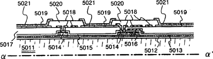
At first, with reference to figure 1 this embodiment of explanation.Herein, luminescent device produces panchromatic demonstration, and the source region or the drain region that wherein are used to the drive TFT of the pixel R that glows are connected to red current source line, the source region or the drain region of drive TFT that is used for the pixel G of green light is connected to green current source line, and the source region or the drain region of drive TFT that is used for the pixel B of blue light-emitting is connected to blue current source line.The EL material of the EL element of R, G, B is striated independently and uses.
Among Fig. 1, dividing wall covers all districts except that luminous zone 5007.Between dividing wall 5020, with the dividing wall of the parallel formation of described striped as the color edge.Exist dividing wall can not be used as the luminous zone as the place at color edge.Therefore, source signal line 5001 and current source line 5003 are arranged in below the dividing wall.Then, drive TFT 5005 is arranged in below the source signal line 5001 and below the current source line 5003.Herein, they can be arranged on below the source signal line and current source line that neighbor has.
In the present embodiment, the grid of drive TFT and current source line overlaps.Current source line is at be fixed on if having time predetermined potential.Therefore, the grid of drive TFT and current source line can be as parts that keeps capacitor C s.
Drive TFT 5005 has the channel length of lengthening and the channel width of widening, thereby also as maintenance electric capacity, and the variation of rejection characteristic.But,,,, can not reduce the aperture ratio although the channel length of lengthening and the channel width of widening are then arranged as the color edge in case drive TFT 5005 is arranged in below the dividing wall yet.
When constituting pixels with 3 transistors, two transistors, promptly switching TFT and erasing TFT do not comprise drive TFT, linear array keeping the aperture ratio, thereby realizes the opening portion further simplified.The opening portion of approximate rectangular simple shape helps to reduce contractive effect.
Embodiment 3
When the channel length of determining drive TFT and channel width, must increase channel length and channel width as far as possible, and when drive TFT will be operated in the saturation region, must the selection channel length greater than channel width, make gate source voltage V
GSBe subjected to the influence of threshold voltage hardly.In case increased channel length, the characteristic of drive TFT will be more level and smooth in the saturation region.Herein, if gate source voltage V
GSIncrease too much, will produce the problem relevant with voltage breakdown with the power consumption of drive TFT.Therefore, preferably regulate channel length and channel width, make | V
GS| be not less than 4V, and be not more than 14V.
According to embodiment 1-3, the size of drive TFT strengthens, and channel length L increases with respect to channel width W, makes to use to have the drive TFT of the TFT of good homogeneous current characteristics as pixel in the saturation region, and prevents the influence that the brightness of EL element is changed by drive TFT.
In addition, keep electric capacity to be produced by the channel capacitance of drive TFT, and be arranged in a position outside the luminous zone, in this position, itself and dividing wall are overlapping.Therefore, can expect higher aperture ratio.
Embodiment 4
The luminescence efficiency of the EL element of R, G, B is different mutually usually.Therefore, the current characteristics of drive TFT is just the same, in order to produce the difference between the current value, and the V that requires in drive TFT
GSProduce different between the value.Therefore, when the luminescence efficiency difference of the EL element of every kind of R, G, B is big, V
GSDifference between the value may be bigger, and voltage is set may be very difficult.
In this case, preferably, regulate current characteristics by change the channel length/channel width of drive TFT corresponding to R, G, B light-emitting component.Herein, by regulate the channel length and the channel width of drive TFT in a scope, the aperture of R, G, B light-emitting component is than just the same, and wherein, in described scope, drive TFT does not exceed the zone of the dividing wall that is used for the color edge.And, by regulating the ratio of channel length/channel width, make its increase corresponding to every kind of R, G, B light-emitting component, can fully obtain channel capacitance.
For example
Working example of the present invention is described below.
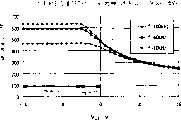
Example 1
Figure 13 illustrates the actual grid that record-source electric capacity and grid-drain capacitance.Gate source voltage V
GSMaintain-6V drain source voltage V
DS16V and-change between the 16V.Work as V
DSBecome approximately-5V or when lower, begin to enter the saturation region.The summation of the grid among Figure 13 A and the 13B-source electric capacity and grid-drain capacitance is the capacity of drive TFT.
When drive TFT when linear zone is driven, shown in Figure 17 C, on whole semiconductor surface, form raceway groove, and can keep enough electric capacitys.
When drive TFT was driven in the saturation region, shown in Figure 17 C, one end did not form raceway groove in the drain region, and grid-drain capacitance presents 0 the value of being approximately shown in Figure 13 B.But, because one end forms raceway groove in the source region, can be by grid-abundant building-out capacitor of source electric capacity as shown in FIG. 13A.Therefore, when being desirably in saturation region driving drive TFT, can keep the channel capacitance of q.s by using P channel-type drive TFT.
According to the above, in pixel, do not form big maintenance electric capacity, high aperture ratio is to obtain by the channel capacitance that uses drive TFT.In addition, the product that increases channel length and channel width helps the unified semi-conductive crystallinity that constitutes drive TFT to change, thus the conducting electric current I of straining element
OnVariation.
Even when drive TFT is driven in the saturation region, the V about the drive TFT in the pixel also can take place
GS-I
DSThe problem of characteristic variations.In this case, the electric current that flows into EL element remains unchanged, but that channel length is added to is enough bigger than channel width, thereby improves the saturation characteristic in the saturation region.On the other hand, after the increase channel length, the electric current that acts on EL element just reduces.Therefore, by increasing gate source voltage V
GSCome to provide the electric current of expectation to EL element.Therefore, gate source voltage V
GSBecome fully greater than threshold voltage the influence that this is changed hardly, leakage-source electric current I
DSIn variation further reduce.Because saturation characteristic is improved leakage-source electric current I because of increasing channel length
DSAlmost remain unchanged in the saturation region.Therefore, even resistance changes owing to the degeneration of EL element, also can provide the electric current of amount much at one to EL element.
Figure 14 illustrates increases channel length and channel width, and channel length relatively and channel width when fully increasing, the measurement electric current I of TFT
DSVariation.
Gate source voltage | V
GS| be fixed as 5V, drain source voltage | V
DS| be fixed as 8V, measure grid-source electric current I by using a plurality of elements with different channel lengths and channel width
DSBe appreciated that grid-source electric current I from Figure 14
DSIn variation can suppress by the area (channel length * channel width) that increases channel formation region.With 5V in Figure 14 | V
GS| with comparing of 8V, find to work as V
GSMuch larger than V
ThThe time, I
DSVariation suppressed.
Example 2
The structure and the planimetric map of 2 transistor-type pixels are described below with reference to Fig. 1.
The pixel of Fig. 1 is by source signal line 5001, signal line 5002, current source line 5003, switching TFT 5004, drive TFT 5005, pixel electrode 5006 and covering other regional dividing wall except that luminous zone 5007.The grid of switching TFT 5004 connects signal line 5002, and its source terminal connects source signal line 5001, and drain electrode end connects current source line 5003.In addition, the source terminal of drive TFT 5005 connects current source line 5003, and its drain electrode end connects pixel electrode 5006.
Between the dividing wall that covers other district except that luminous zone 5007, the dividing wall that provides between the neighbor of the left and right sides is as the color edge, and when independent generation R, G, B color, this color edge is necessary.The width of the dividing wall that provides between the neighbor of the left and right sides is preferably 30 μ m.
Herein, the dividing wall as the color edge can not be used as the luminous zone.Therefore, source signal line 5001 and current source line 5003 are arranged in below the wide dividing wall of 30 μ m.Then, drive TFT 5005 is arranged in below source signal line 5001 and the current source line 5003.Herein, drive TFT 5005 can be arranged in below the source signal line and current source line that neighbor has.
Keep electric capacity to realize by the channel capacitance that produces by first mesosphere insulation film 5017 between the grid 5016 of semiconductor layer 5014 and drive TFT 5005.
Herein, the retention time is made as 1ms, the I of drive TFT
OffDigital gradient by short hold period is made as 1pA, when the brightness of EL element changes a gradient, and the gate source voltage V of drive TFT
GSVariation delta V
GSBe made as about 0.02V.According to formula (3), necessary maintenance electric capacity is 50fF.If the thickness of grid insulating film 5015 is chosen as 120nm, concrete specific inductive capacity is 4, and then channel capacitance is about 60fF, channel length * channel width=200 μ m
2Like this, in order to obtain satisfied electric capacity, best channel length * channel width=200 μ m
2Or it is more.
In addition, along with the increase of the channel length * channel width of drive TFT 5005, the variation of element reduces.Therefore, preferably channel length and channel width are big as far as possible.
When drive TFT 5005 was driven in the saturation region, expectation selected channel length greater than channel width, made V
GSBe subjected to the influence of threshold voltage hardly.Herein, expectation channel length/channel width is not less than 5.After increasing channel length, drive TFT can be more level and smooth in the characteristic of saturation region.But, if gate source voltage V
GSIncrease too much, can occur about the power consumption of drive TFT and the problem of voltage breakdown.Therefore, preferably regulate channel length and channel width, make | V
GS| be not less than 4V, and be not more than 14V.
The channel length of drive TFT 5005 can be by stretching increasing on the vertical direction of being represented by semiconductor layer 5014.The channel length of drive TFT 5005 can increase, and channel width also can increase to a certain extent, and can not reduce the aperture ratio.
When the aperture when high, the current density of EL element reduces, thereby has guaranteed the long-life.In addition, because the opening portion simple shape, contractive effect also reduces.
Fig. 2 A illustrates the example of a semiconductor layer, and its pattern form is different with the semiconductor layer of Figure 1A.Fig. 2 B is along the sectional view of α-α ' among Fig. 2 A.Semiconductor layer can be crooked on the vertical direction of drive TFT 5105 expressions.Because semiconductor layer forms like this, the channel length of drive TFT 5105 can further increase, and can not reduce the aperture ratio.
Fig. 3 A illustrates the example of a semiconductor layer, and its pattern form is different with the semiconductor layer of Figure 1A.Fig. 3 B is along the sectional view of α-α ' among Fig. 3 A.Semiconductor layer can constitute the U-shaped as drive TFT 5205 expressions.Because semiconductor layer forms like this, the channel length of drive TFT 5205 can further increase, and channel width also can increase to a certain extent, and can the smaller aperture due ratio.
Fig. 4 A illustrates the example of a semiconductor layer, and its pattern form is different with the semiconductor layer of Figure 1A.Fig. 4 B is along the sectional view of α-α ' among Fig. 4 A.Semiconductor layer can form shape crooked on the horizontal direction of drive TFT 5305 expressions.Herein, the meaning of " bending " is " mode with bending flows ", and the shape of " crooked shape " expression semiconductor layer is crooked.Because semiconductor layer forms like this, the channel length of drive TFT 5305 can further increase, and channel width also can increase to a certain extent, and can not reduce the aperture ratio.
Example 3
The structure and the planimetric map of 3 transistor-type pixels are described below with reference to Fig. 5.
Increased and be used for the erasing transistor 5506 that SES drives, the grid of this erasing transistor connects the second grid signal wire 5503 to grid input erase signal, source electrode connects current source line 5504, and drain electrode connects the drain electrode of switching TFT 5505 and the grid of drive TFT 5507.
Under the situation of 3 transistor-type pixels, two TFT, that is: switching TFT 5505 and erasing TFT 5506 linearities are arranged side by side between first grid signal wire 5502 and the second grid signal wire 5503.The drain region of switching TFT 5505 can be overlapping with the drain region of erasing TFT 5506.Herein, switching transistor and erasing transistor are arranged at such position, make the point in switching TFT 5505 source regions and a point in drain region, and a point in point in erasing TFT 5506 source regions and drain region is arranged point-blank.
This arrangement makes and might improve the aperture ratio and simplify opening portion.
Fig. 6 A illustrates the example of a semiconductor layer, and its pattern form is different with the semiconductor layer of Fig. 5 A.Fig. 6 B is along the sectional view of α-α ' among Fig. 6 A.Semiconductor layer can be crooked on the vertical direction of drive TFT 5607 expressions.Because semiconductor layer forms like this, the channel length of drive TFT 5607 can further increase, and can not reduce the aperture ratio.
Fig. 7 A illustrates the example of a semiconductor layer, and its pattern form is different with the semiconductor layer of Fig. 5 A.Fig. 7 B is along the sectional view of α-α ' among Fig. 7 A.Semiconductor layer can constitute the U-shaped as drive TFT 5707 expressions.Because semiconductor layer forms like this, the channel length of drive TFT 5707 can further increase, and channel width also can increase to a certain extent, and can the smaller aperture due ratio.
Fig. 8 A illustrates the example of a semiconductor layer, and its pattern form is different with the semiconductor layer of Fig. 5 A.Fig. 8 B is along the sectional view of α-α ' among Fig. 8 A.Semiconductor layer can form by drive TFT 5807 expression curved shapes.Because semiconductor layer forms like this, the channel length of drive TFT 5807 can further increase, and channel width also can increase to a certain extent, and can not reduce the aperture ratio.
Figure 10 A illustrates the example of a semiconductor layer, and its pattern form is different with the semiconductor layer of Fig. 5 A.Figure 10 B is along the sectional view of α-α ' among Figure 10 A.The size of the semiconductor layer of drive TFT is shown in 5907.When the grid capacitance that only relies on drive TFT, when keeping electric capacity big inadequately, can form maintenance electric capacity 5910.After below dividing wall 5920, forming maintenance electric capacity 5910, can obtain fully big maintenance electric capacity, and can not reduce the aperture ratio.
In the pixel of structure shown in example 2 and this example, drive TFT is operated in the saturation region, with the gate source voltage that only depend on drive TFT of control action in EL element, and with the irrelevant electric current of the source-drain voltage of drive TFT.In this case, drive TFT is as current source.Therefore, need not form current source circuit, or current source circuit is added on the driving circuit that externally provides, help to reduce size of devices like this at the peripheral whole of pixel portion of luminescent device.
Example 4
With reference to figure 9A, in being included in such as the electronic equipment of mobile phone etc., luminescent device during as display unit, is changed to the form of module 901 in it.Herein, a kind of module of module 901 expression, in this module, luminescent device is connected to a template, and the signal Processing LSI, storer of driven for emitting lights device etc. are installed on this template.
Fig. 9 B is the block scheme of module 901.Module 901 comprises power supply unit 911, signaling control unit 912, FPC 913 and luminescent device 914.Power supply unit 911 is constituted the voltage of a plurality of expectations, and is provided it to source signal line drive circuit, signal line drive circuit, luminescent device etc. by the external cell power supply.Signaling control unit 912 receiving video signals and synchronizing signal are converted into various signals, so that handled by luminescent device 901, and form clock signal etc., are used to drive source electrode signal-line driving circuit and signal line drive circuit.
The module 901 of present embodiment comprises independent luminescent device 914, power supply unit 911 and the signaling control unit 912 that forms.But they also can whole formation on a substrate.
Figure 11 is shown specifically the structure of the luminescent device 914 that comprises in the module 901 shown in Figure 9.
Described luminescent device is on template 1001, with pixel portion 1003, source signal line drive circuit 1004, signal line drive circuit 1005 and 1006 and formation such as FPC 1007.Relative template 1002 can be made of transparent material such as glass or metal material.Gap between template 1001 and the relative template 1002 seals with filling agent, and is filled with drying agent usually, in case EL element is bad by damage by water.
Figure 11 B is a top view.Middle body at substrate is arranged pixel portion 1003.Arrange to have source electrode signal-line driving circuit 1004 and signal line drive circuit 1005 and 1006 in the periphery.Current source line 1011 and reverse electrode contact 1013 etc. are arranged to have in periphery at source signal line drive circuit 1004.On the whole surface of pixel portion, form the reverse electrode of EL element, and by FPC 1007, the 1013 effect reverse potentials from the reverse electrode contact.Be used to drive source electrode signal-line driving circuit 1004 and signal line drive circuit 1005 and 1006 and the signal of power supply provide from external unit by FPC 1007.
It is overlapping with source signal line drive circuit 1004 that the seal element 1014 of electrode 1001 and reverse electrode 1002 of being used to bond can become part, and on signal line drive circuit 1005 and 1006, shown in Figure 11 B.Like this, the framework of light-emitting component can narrow down.
Example 5
In example 5, a kind of example that uses the present invention to make luminescent device is described with reference to figure 19A-19C.
Figure 19 A is the top view of a luminescent device, and this luminescent device forms by sealing a transistor chip, on this substrate, provides a pixel portion by encapsulant.Figure 19 B is the sectional view along the A-A ' line among Figure 19 A, and Figure 19 C is the sectional view along the B-B ' line among Figure 19 A.
First and second signal line drive circuit 4004a and the 4004b that seal member 4009 surrounds pixel portion 4002, source signal line drive circuit 4003 and provides on substrate 4001.In addition, on pixel portion 4002, source signal line drive circuit 4003 and the first and second signal line drive circuit 4004a and 4004b, provide seal member 4008.Like this, pixel portion 4002, source signal line drive circuit 4003 and the first and second signal line drive circuit 4004a and 4004b just and filling agent 4210 be sealed by substrate 4001, seal member 4009 and seal member 4008.Seal member 4009 can with the overlapping of source signal line drive circuit 4003 and the first and second signal line drive circuit 4004a and 4004b.
In addition, the pixel portion 4002 that provides on substrate 4001, source signal line drive circuit 4003 and the first and second signal line drive circuit 4004a and 4004b comprise a plurality of TFT.Figure 19 B typically illustrates the TFT 4202 that comprises in TFT (a n channel TFT and a p channel TFT are shown) 4201 that comprise in the source signal line drive circuit 4003 and the pixel portion 4002 herein.
At insulation film (flat film) 4301 between cambium layer on drive TFT 4201 and 4202, form the pixel electrode (anode) 4203 in the drain region that is electrically connected TFT4202 thereon.Transparent conductive film with high work function is as pixel electrode 4203.The potpourri of the potpourri of indium oxide and tin oxide, indium oxide and zinc paste, zinc paste, tin oxide or indium oxide can be used as this transparent conductive film.In addition, also can use the transparent conductive film that adds gallium.
On pixel electrode 4203, form insulation film 4302, form opening portion in the insulation film 4302 on pixel electrode 4203.In this opening portion, on pixel electrode 4203, form organic luminous layer 4204.Organic luminous layer 4204 is to utilize known luminous organic material or phosphor to form.Although luminous organic material comprises low molecular system (monomer system) and polymer system (polymer system), two kinds can be used.
Organic luminous layer 4204 is to utilize known evaporation technique or paint-on technique to make.This organic luminous layer can be made stepped construction, comprises hole injection layer, hole transmission layer, luminescent layer, electron transfer layer and an electron injecting layer, or single layer structure.
On organic luminous layer 4204, make negative electrode 4205 with shading characteristic with conducting membranes (typically, the Main Ingredients and Appearance of conducting membranes is aluminium, copper or silver, or the stack film of these and other conducting membranes).Preferably remove the moisture and the oxygen that exist on the interface between negative electrode 4205 and the organic luminous layer 4204 as far as possible.Therefore, must take such way, make organic luminous layer 4204 in nitrogen or rare gas environment, form, and negative electrode 4205 is not exposed at luminescent layer under the condition of oxygen or moisture and forms.In this example, adopted multi-chamber system (cluster tool system) film forming device, made and to carry out above-mentioned thin film fabrication.Predetermined voltage acts on negative electrode 4205.
According to the above, form the light-emitting component 4303 that comprises pixel electrode (anode) 4203, organic luminous layer 4204 and negative electrode 4205.Then, on insulation film 4302, form protection mould 4209, with covering luminous element 4303.Protection mould 4209 can effectively prevent intrusion light-emitting components 4303 such as oxygen, moisture.
But, pointing under the situation of coating member in the radiation direction of the light that light-emitting component sends, coating member must be transparent.In this case, adopt transparent material, as glass plate, plastic plate, polyester (polyester) film or acryl film.
For filling agent 4103, except inert gas such as nitrogen or argon gas, can also use resin, PVC (polyvinyl chloride), acryl, polyimide, epoxy resin, silicones, PVB (polyvinyl butyral) or the EVA (vinyl acetic acid esters) of UV cured resin or thermmohardening.In this example, use nitrogen as filling agent.
In addition, maybe can absorb in the material of oxygen for filling agent 4103 being exposed to hygroscopic material (preferably baryta), provide a sunk part 4007 on substrate 4001 side seal parts 4008 surfaces, the material 4207 that hygroscopic material maybe can absorb oxygen is placed in one.Then, maybe can absorb material 4207 diffusions of oxygen, the material that hygroscopic material maybe can absorb oxygen be remained in the sunk part 4007 with depression coating member 4208 in order to prevent hygroscopic material.Notice that depression coating member 4208 is made the fine mesh structure, air and moisture can pass, and hygroscopic material maybe can absorb the material 4207 of oxygen and can not pass.By the material 4207 that provides hygroscopic material maybe can absorb oxygen, can suppress light-emitting component 4303 and degenerate.
Shown in Figure 19 C, when forming pixel electrode 4203, form the conducting membranes 4203a that is connected with stretching lead 4005a.
Example 6
In the example 6, the manufacturing step of the luminescent device shown in example 2 and the example 3 is described with reference to figure 22A-22D.Although only provide the explanation of pixel portion herein, the manufacturing step of driving circuit is not limited thereto, so it is described in omission herein.
Shown in Figure 22 A,,, form the substrate film (not shown) of making by silicon oxide film, silicon nitride film or silicon oxynitride film on the substrate of making as barium borosilicate glass or alumina borosilicate glass by glass.Then, utilize laser crystallization method and known amorphous semiconductor layer of thermal crystallisation method crystallization.Then, on the semiconductor layer of crystallization, form pattern, to obtain semiconductor island 2201 and 2201 (Figure 22 A).
Form the grid insulating film (not shown) to cover semiconductor island 2201 and 2202.The conductor thin film that forms grid can be by being selected from Ta, W, Ti.The element of Mo, Al, Cu or mainly comprise the alloy material of above-mentioned element, or comprise that mainly the composite material of above-mentioned element makes.Then, form the pattern of intended shape, to obtain grid 2203 and 2204 (reference number 2203 had both been represented grid, represented the signal line again) (Figure 22 B).
Form also in order to make smooth insulation film (not shown) of substrate surface and pixel electrode 2205 thereon.In pixel electrode 2205, be under the situation of upper surface at display surface, electrode is a reflecting electrode, is under the situation of lower surface at display surface, electrode is a transparency electrode.MgAg etc. can be as the typical material that forms this transparency electrode.After forming film, pixel electrode 2205 is made the shape of expectation by the needle drawing case with above-mentioned material.
Form to arrive the opening of semiconductor layer 2201,2202 and grid 2204, to make lead 2207-2209 (reference number 2207 is the source signal line, the 2208th, current source line).Lead 2209 is overlapped to contact (Figure 22 C) with pixel electrode 2206.
Then, between adjacent pixels, form dividing wall, and open part (Figure 22 D) as luminous zone 2210 by etching.Then, on opening portion, form the EL layer, thereby finish pixel portion.
Example 7
Luminescent device of the present invention is an emissive type, so, compare with liquid crystal display device, but present the better identification of shown image, and have wideer visual angle in bright place.Therefore, luminescent device can be used for the display part of various electronic equipments.
Use the electronic equipment of luminescent device of the present invention to comprise video camera, digital camera, glasses type display (head mounted display), navigational system, sound reproduction equipment (as vehicle-mounted voice band device and audio set), kneetop computer, game machine, portable data assistance (as: removable computer, mobile phone, portable game machine and e-book), comprise that recording medium (particularly, it is the device that can reappear recording medium, as digital universal disc (DVD) etc., and comprise a display, be used for showing the image of reproduction) image reconstructor etc.Especially, under the situation of portable data assistance, preferably use this luminescent device, because often will require to have wide visual angle usually from the portable data assistance that the angle that tilts is watched.Figure 21 A-21H illustrates the example of various electronic equipments respectively.
Figure 21 A illustrates a kind of electro-luminescence display device, comprises an overcoat 3001, brace table 3002, display part 3003, speaker portion 3004, video inputs 3005 etc.The present invention can be used for display part 3003.Luminescent device is an emissive type, therefore, does not require backlight.Like this, the thickness of display part can be thinner than liquid crystal display.Luminescent device comprises the whole display device that is used for display message, as personal computer, television broadcast receiver or advertisement display.
Figure 21 B illustrates a digital still camera, comprises main body 3101, display part 3102, image receiving unit 3103, operating key 3104, external connection port 3105, shutter 3106 etc.Luminescent device of the present invention can be used as display part 3102.
Figure 21 C illustrates a kneetop computer, comprises main body 3201, overcoat 3202, display part 3203, keyboard 3204, external connection port 3205, gives directions mouse 3206 etc.Luminescent device of the present invention can be used as display part 3203.
Figure 21 D illustrates mobile computer, comprises main body 3301, display part 3302, switch 3303, operating key 3304, infrared port 3305 etc.Luminescent device of the present invention can be used as display part 3302.
Figure 21 E illustrates a kind of portable image reproducer that has a recording medium (more specifically, be the DVD reproducer), comprise main body 3401, overcoat 3402, display part A3403, another display part B3404, recording medium (DVD etc.) reading section 3405, operating key 3406, speaker portion 3407 etc.Display part A3403 is mainly used in displays image information, and display part B3404 is mainly used in character display information.Luminescent device of the present invention can be used as display part A3403 and display part B3404.The image reconstructor that comprises recording medium also comprises family game machine etc.
Figure 21 F illustrates a glasses type display (head mounted display), comprises main body 3501, display part 3502, support arm portion 3503 etc.Luminescent device of the present invention can be used as display part 3502.
Figure 21 G illustrates a video camera, comprises main body 3601, display part 3602, overcoat 3603, external connection port 3604, Long-distance Control receiving unit 3605, image receiving unit 3606, battery 3607, sound importation 3608, operating key 3609 etc.Luminescent device of the present invention can be used as display part 3602.
Figure 21 H illustrates a mobile phone, comprises main body 3701, overcoat 3702, display part 3703, sound importation 3704, voice output part 3705, operating key 3706, external connection port 3707, antenna 3708 etc.Luminescent device of the present invention can be used as display part 3703.Notice that by display white symbol on black background, power consumption can be reduced in the display part 3703 of mobile phone.
When in the future obtaining the brighter light time from luminous organic material, luminescent device of the present invention can be used for orthogonal projection machine or back reflection projector, and wherein, the light that comprises output image information is by amplifications such as lens, and cast out.
Aforementioned electronic equipment more may be used for showing the information of propagating by telecommunication such as internet, CATV (cable television system) etc., may be used to show moving image information especially.Luminescent device of the present invention is fit to show moving image information, because luminous organic material can present than high response speed.
The luminous component consumed energy of luminescent device, so best display message by this way, that is: luminous component wherein is as far as possible little.Therefore, when luminescent device is used for the display part of main character display information, display part as personal digital assistant device, more specifically, as portable phone or sound reproduction equipment, preferably drive described luminescent device, make character information form by luminous component, and not luminous component corresponding to background.
As mentioned above, the present invention can differently be used for the various electronic of all spectra.And the electronic equipment in this example can make any structure of the luminescent device in the use-case 1-example 6 realize.
According to foregoing invention, the size of drive TFT increases, and channel length L also increases with respect to channel width W, makes to use the drive TFT of the TFT of the current characteristics that has good homogeneity in the saturation region as pixel, and prevents the influence that the brightness of EL element is changed by drive TFT.In addition, keep electric capacity to be produced by the channel capacitance of drive TFT, and be arranged in a position, in this position, it is overlapping with luminous zone isolation arm in addition.Therefore, can obtain high aperture ratio.
Claims (71)
1. luminescent device comprises:
A plurality of pixels, each pixel comprises:
A light-emitting component; With
A driving transistors;
Wherein, be used for keeping the capacitor of the gate source voltage of each driving transistors to constitute by the grid of driving transistors, the channel formation region of semiconductor layer and insulation film therebetween.
2. luminescent device comprises:
A plurality of pixels, each pixel comprises:
A light-emitting component; With
A driving transistors;
Wherein, be used for keeping the capacitor of the gate source voltage of each driving transistors to be made of at least one of following two kinds of electric capacity: a kind of electric capacity comprises the grid of each driving transistors, the source region in the semiconductor layer and the insulation film between grid and the source region; Another kind of electric capacity comprises the insulation film between grid, the drain region in the semiconductor layer and the grid and the drain region of each driving transistors.
3. luminescent device comprises:
A plurality of pixels, each pixel comprises:
A light-emitting component;
A switching transistor;
An erasing transistor; With
A driving transistors;
Wherein, be used for keeping the capacitor of the gate source voltage of each driving transistors to constitute by the grid of each driving transistors, the channel formation region of semiconductor layer and the insulation film between grid and the channel formation region.
4. luminescent device comprises:
A plurality of pixels, each pixel comprises:
A light-emitting component;
A switching transistor;
An erasing transistor; With
A driving transistors;
Wherein, be used for keeping the capacitor of the gate source voltage of each driving transistors to be made of at least one of following two kinds of electric capacity: a kind of electric capacity comprises the grid of each driving transistors, the source region in the semiconductor layer and the insulation film between grid and the source region; Another kind of electric capacity comprises the insulation film between grid, the drain region in the semiconductor layer and the grid and the drain region of each driving transistors.
5. luminescent device comprises:
Many source signal lines;
Many current source lines;
A plurality of pixels, each pixel comprises:
A plurality of luminescent devices, each luminescent device comprise a luminous zone; With
A plurality of driving transistorss, each driving transistors is corresponding to a light-emitting component;
Wherein, source signal line, current source line and driving transistors are arranged to insulation film overlapping, and this film forms in the position of the adjacent luminous zone of isolate pixels.
6. luminescent device comprises:
Many source signal lines;
Many current source lines;
A plurality of pixels, each pixel comprises:
A plurality of luminescent devices, each luminescent device comprise a luminous zone;
A plurality of switching transistors, each switching transistor is corresponding to a light-emitting component;
A plurality of erasing transistors, each erasing transistor is corresponding to a light-emitting component; With
A plurality of driving transistorss, each driving transistors is corresponding to a light-emitting component;
Wherein, many source signal lines, many current source lines and a plurality of driving transistors are arranged to insulation film overlapping, and this film forms in the position of the adjacent luminous zone of isolate pixels.
7. according to the luminescent device of claim 3, wherein, each switching transistor and each erasing transistor are arranged in such position, make the point in each switching transistor source region and a point in drain region, and a point in point in each erasing transistor source region and drain region is arranged in the position that all comprises point-blank.
8. according to the luminescent device of claim 4, wherein, each switching transistor and each erasing transistor are arranged in such position, make the point in each switching transistor source region and a point in drain region, and a point in point in each erasing transistor source region and drain region is arranged in the position that all comprises point-blank.
9. according to the luminescent device of claim 6, wherein, each switching transistor and each erasing transistor are arranged in such position, make the point in each switching transistor source region and a point in drain region, and a point in point in each erasing transistor source region and drain region is arranged in the position that all comprises point-blank.
10. according to the luminescent device of claim 5, wherein, each driving transistors is arranged at such position, and in this position, each driving transistors is with one of the part of every source signal line and part of every current source line are overlapping at least.
11. according to the luminescent device of claim 6, wherein, each driving transistors is arranged at such position, in this position, each driving transistors is with one of the part of every source signal line and part of every current source line are overlapping at least.
12. according to the luminescent device of claim 1, wherein, the shape of each semiconductor layer of the channel region of formation driving transistors is selected from U-shaped, S shape, spirality and indentation.
13. according to the luminescent device of claim 2, wherein, the shape of each semiconductor layer of the channel region of formation driving transistors is selected from U-shaped, S shape, spirality and indentation.
14. according to the luminescent device of claim 3, wherein, the shape of each semiconductor layer of the channel region of formation driving transistors is selected from U-shaped, S shape, spirality and indentation.
15. according to the luminescent device of claim 4, wherein, the shape of each semiconductor layer of the channel region of formation driving transistors is selected from U-shaped, S shape, spirality and indentation.
16. according to the luminescent device of claim 5, wherein, the shape of each semiconductor layer of the channel region of formation driving transistors is selected from U-shaped, S shape, spirality and indentation.
17. according to the luminescent device of claim 6, wherein, the shape of each semiconductor layer of the channel region of formation driving transistors is selected from U-shaped, S shape, spirality and indentation.
18. according to the luminescent device of claim 1, wherein, the channel length of each driving transistors is L, channel width is W, and
Wherein, L * W>200 μ m
2
19. according to the luminescent device of claim 2, wherein, the channel length of each driving transistors is L, channel width is W, and
Wherein, L * W>200 μ m
2
20. according to the luminescent device of claim 3, wherein, the channel length of each driving transistors is L, channel width is W, and
Wherein, L * W>200 μ m
2
21. according to the luminescent device of claim 4, wherein, the channel length of each driving transistors is L, channel width is W, and
Wherein, L * W>200 μ m
2
22. according to the luminescent device of claim 5, wherein, the channel length of each driving transistors is L, channel width is W, and
Wherein, L * W>200 μ m
2
23. according to the luminescent device of claim 6, wherein, the channel length of each driving transistors is L, channel width is W, and
Wherein, L * W>200 μ m
2
24. according to the luminescent device of claim 1, wherein, the gate source voltage of driving transistors is V
GS, source-drain voltage is V
DS, threshold voltage is V
Th, and
Wherein, driving transistors is driven like this, that is: | and V
DS|<| V
GS|-| V
Th|.
25. according to the luminescent device of claim 2, wherein, the gate source voltage of driving transistors is V
GS, source-drain voltage is V
DS, threshold voltage is V
Th, and
Wherein, driving transistors is driven like this, that is: | and V
DS|<| V
GS|-| V
Th|.
26. according to the luminescent device of claim 3, wherein, the gate source voltage of driving transistors is V
GS, source-drain voltage is V
DS, threshold voltage is V
Th, and
Wherein, driving transistors is driven like this, that is: | and V
DS|<| V
GS|-| V
Th|.
27. according to the luminescent device of claim 4, wherein, the gate source voltage of driving transistors is V
GS, source-drain voltage is V
DS, threshold voltage is V
Th, and
Wherein, driving transistors is driven like this, that is: | and V
DS|<| V
GS|-| V
Th|.
28. according to the luminescent device of claim 5, wherein, the gate source voltage of driving transistors is V
GS, source-drain voltage is V
DS, threshold voltage is V
Th, and
Wherein, driving transistors is driven like this, that is: | and V
DS|<| V
GS|-| V
Th|.
29. according to the luminescent device of claim 6, wherein, the gate source voltage of driving transistors is V
GS, source-drain voltage is V
DS, threshold voltage is V
Th, and
Wherein, driving transistors is driven like this, that is: | and V
DS|<| V
GS|-| V
Th|.
30. according to the luminescent device of claim 1, wherein, the gate source voltage of driving transistors is V
GS, source-drain voltage is V
DS, threshold voltage is V
Th, and
Wherein, driving transistors is driven like this, that is: | and V
DS| 〉=| V
GS|-| V
Th|, and | V
GS| be not less than 4V, but be not more than 14V.
31. according to the luminescent device of claim 2, wherein, the gate source voltage of driving transistors is V
GS, source-drain voltage is V
DS, threshold voltage is V
Th, and
Wherein, driving transistors is driven like this, that is: | and V
DS| 〉=| V
GS|-| V
Th|, and | V
GS| be not less than 4V, but be not more than 14V.
32. according to the luminescent device of claim 3, wherein, the gate source voltage of driving transistors is V
GS, source-drain voltage is V
DS, threshold voltage is V
Th, and
Wherein, driving transistors is driven like this, that is: | and V
DS| 〉=| V
GS|-| V
Th|, and | V
GS| be not less than 4V, but be not more than 14V.
33. according to the luminescent device of claim 4, wherein, the gate source voltage of driving transistors is V
GS, source-drain voltage is V
DS, threshold voltage is V
Th, and
Wherein, driving transistors is driven like this, that is: | and V
DS| 〉=| V
GS|-| V
Th|, and | V
GS| be not less than 4V, but be not more than 14V.
34. according to the luminescent device of claim 5, wherein, the gate source voltage of driving transistors is V
GS, source-drain voltage is V
DS, threshold voltage is V
Th, and
Wherein, driving transistors is driven like this, that is: | and V
DS| 〉=| V
GS|-| V
Th|, and | V
GS| be not less than 4V, but be not more than 14V.
35. according to the luminescent device of claim 6, wherein, the gate source voltage of driving transistors is V
GS, source-drain voltage is V
DS, threshold voltage is V
Th, and
Wherein, driving transistors is driven like this, that is: | and V
DS| 〉=| V
GS|-| V
Th|, and | V
GS| be not less than 4V, but be not more than 14V.
36. according to the luminescent device of claim 1, wherein, the channel length of each driving transistors is L, channel width is W, and
Wherein, L>5W.
37. according to the luminescent device of claim 2, wherein, the channel length of each driving transistors is L, channel width is W, and
Wherein, L>5W.
38. according to the luminescent device of claim 3, wherein, the channel length of each driving transistors is L, channel width is W, and
Wherein, L>5W.
39. according to the luminescent device of claim 4, wherein, the channel length of each driving transistors is L, channel width is W, and
Wherein, L>5W.
40. according to the luminescent device of claim 5, wherein, the channel length of each driving transistors is L, channel width is W, and
Wherein, L>5W.
41. according to the luminescent device of claim 6, wherein, the channel length of each driving transistors is L, channel width is W, and
Wherein, L>5W.
42. according to the luminescent device of claim 1,
Wherein, luminescent device glow, a kind of light in green glow and the blue light;
Wherein, the channel length of each driving transistors is L, and channel width is W, and
Wherein, corresponding to the L/W of the driving transistors of the luminescent device of ruddiness, different mutually with L/W corresponding to the driving transistors of the luminescent device of blue light corresponding to the L/W of the driving transistors of the luminescent device of green glow.
43. according to the luminescent device of claim 2,
Wherein, luminescent device glow, a kind of light in green glow and the blue light;
Wherein, the channel length of each driving transistors is L, and channel width is W, and
Wherein, corresponding to the L/W of the driving transistors of the luminescent device of ruddiness, different mutually with L/W corresponding to the driving transistors of the luminescent device of blue light corresponding to the L/W of the driving transistors of the luminescent device of green glow.
44. according to the luminescent device of claim 3,
Wherein, luminescent device glow, a kind of light in green glow and the blue light;
Wherein, the channel length of each driving transistors is L, and channel width is W, and
Wherein, corresponding to the L/W of the driving transistors of the luminescent device of ruddiness, different mutually with L/W corresponding to the driving transistors of the luminescent device of blue light corresponding to the L/W of the driving transistors of the luminescent device of green glow.
45. according to the luminescent device of claim 4,
Wherein, luminescent device glow, a kind of light in green glow and the blue light;
Wherein, the channel length of each driving transistors is L, and channel width is W, and
Wherein, corresponding to the L/W of the driving transistors of the luminescent device of ruddiness, different mutually with L/W corresponding to the driving transistors of the luminescent device of blue light corresponding to the L/W of the driving transistors of the luminescent device of green glow.
46. according to the luminescent device of claim 5,
Wherein, luminescent device glow, a kind of light in green glow and the blue light;
Wherein, the channel length of each driving transistors is L, and channel width is W, and
Wherein, corresponding to the L/W of the driving transistors of the luminescent device of ruddiness, different mutually with L/W corresponding to the driving transistors of the luminescent device of blue light corresponding to the L/W of the driving transistors of the luminescent device of green glow.
47. according to the luminescent device of claim 6,
Wherein, luminescent device glow, a kind of light in green glow and the blue light;
Wherein, the channel length of each driving transistors is L, and channel width is W, and
Wherein, corresponding to the L/W of the driving transistors of the luminescent device of ruddiness, different mutually with L/W corresponding to the driving transistors of the luminescent device of blue light corresponding to the L/W of the driving transistors of the luminescent device of green glow.
48. a utilization is according to the electronic equipment of the luminescent device of claim 1,
Wherein, this electronic equipment is selected from following electronic equipment group: electroluminescence display device, digital still camera, kneetop computer, mobile computer, the portable image reproducer that comprises recording medium, glasses type display, video camera and mobile phone.
49. a utilization is according to the electronic equipment of the luminescent device of claim 2,
Wherein, this electronic equipment is selected from following electronic equipment group: electroluminescence display device, digital still camera, kneetop computer, mobile computer, the portable image reproducer that comprises recording medium, glasses type display, video camera and mobile phone.
50. a utilization is according to the electronic equipment of the luminescent device of claim 3,
Wherein, this electronic equipment is selected from following electronic equipment group: electroluminescence display device, digital still camera, kneetop computer, mobile computer, the portable image reproducer that comprises recording medium, glasses type display, video camera and mobile phone.
51. a utilization is according to the electronic equipment of the luminescent device of claim 4,
Wherein, this electronic equipment is selected from following electronic equipment group: electroluminescence display device, digital still camera, kneetop computer, mobile computer, the portable image reproducer that comprises recording medium, glasses type display, video camera and mobile phone.
52. a utilization is according to the electronic equipment of the luminescent device of claim 5,
Wherein, this electronic equipment is selected from following electronic equipment group: electroluminescence display device, digital still camera, kneetop computer, mobile computer, the portable image reproducer that comprises recording medium, glasses type display, video camera and mobile phone.
53. a utilization is according to the electronic equipment of the luminescent device of claim 6,
Wherein, this electronic equipment is selected from following electronic equipment group: electroluminescence display device, digital still camera, kneetop computer, mobile computer, the portable image reproducer that comprises recording medium, glasses type display, video camera and mobile phone.
54. according to the luminescent device of claim 3, wherein, switching transistor and erasing transistor linear array.
55. according to the luminescent device of claim 4, wherein, switching transistor and erasing transistor linear array.
56. according to the luminescent device of claim 6, wherein, switching transistor and erasing transistor linear array.
57. a luminescent device comprises:
A thin film transistor (TFT) comprises:
A semiconductor layer, this layer comprise that one is positioned at the channel formation region on the insulating surface, a source region and a drain region;
Grid insulating film on this semiconductive thin film; With
Grid on this grid insulating film;
Layer insulation film on this grid and the grid insulating film;
Source signal line on this layer insulation film;
Current source line on this layer insulation film;
Pixel electrode on this layer insulation film; With
Luminescent layer on this pixel electrode,
Wherein, described thin film transistor (TFT) is overlapping with one of source signal line and current source line at least.
58. a luminescent device comprises:
A thin film transistor (TFT) comprises:
A semiconductor layer, this layer comprise that one is positioned at the channel formation region on the insulating surface, a source region and a drain region;
Grid insulating film on this semiconductive thin film; With
Grid on this grid insulating film;
Layer insulation film on this grid and the grid insulating film;
Source signal line on this layer insulation film, this source signal line contacts with the source region of semiconductor layer;
Current source line on this layer insulation film;
Pixel electrode on this layer insulation film; With
Luminescent layer on this pixel electrode,
Wherein, described thin film transistor (TFT) is overlapping with one of source signal line and current source line at least, and
Wherein, be used to keep the electric capacity of the gate source voltage of described thin film transistor (TFT) to constitute by between the grid of described thin film transistor (TFT) and channel formation region, inserting grid insulating film.
59. a luminescent device comprises:
A thin film transistor (TFT) comprises:
A semiconductor layer, this layer comprise that one is positioned at the channel formation region on the insulating surface, a source region and a drain region;
Grid insulating film on this semiconductive thin film; With
Grid on this grid insulating film;
Layer insulation film on this grid and the grid insulating film;
Source signal line on this layer insulation film, this source signal line contacts with the source region of semiconductor layer;
Current source line on this layer insulation film;
Pixel electrode on this layer insulation film; With
Luminescent layer on this pixel electrode,
Wherein, described thin film transistor (TFT) is overlapping with one of source signal line and current source line at least, and
Wherein, be used for keeping the electric capacity of the gate source voltage of described thin film transistor (TFT) to constitute by at least one of following two kinds of electric capacity: a kind of electric capacity, comprise the grid and the source region of described thin film transistor (TFT), grid insulating film inserts between them; Another kind of electric capacity comprises the grid and the drain region of described thin film transistor (TFT), and grid insulating film inserts between them.
60. according to the luminescent device of claim 57,
Wherein, the shape of semiconductor layer that forms the channel region of described thin film transistor (TFT) is selected from U-shaped, S shape, spirality and indentation.
61. according to the luminescent device of claim 58,
Wherein, the shape of semiconductor layer that forms the channel region of described thin film transistor (TFT) is selected from U-shaped, S shape, spirality and indentation.
62. according to the luminescent device of claim 59,
Wherein, the shape of semiconductor layer that forms the channel region of described thin film transistor (TFT) is selected from U-shaped, S shape, spirality and indentation.
63. according to the luminescent device of claim 57,
Wherein, the channel length of described thin film transistor (TFT) is L, and channel width is W, and
Wherein, L * W>200 μ m
2
64. according to the luminescent device of claim 58,
Wherein, the channel length of described thin film transistor (TFT) is L, and channel width is W, and
Wherein, L * W>200 μ m
2
65. according to the luminescent device of claim 59,
Wherein, the channel length of described thin film transistor (TFT) is L, and channel width is W, and
Wherein, L * W>200 μ m
2
66. according to the luminescent device of claim 57,
Wherein, the channel length of described thin film transistor (TFT) is L, and channel width is W, and
Wherein, L>5W.
67. according to the luminescent device of claim 58,
Wherein, the channel length of described thin film transistor (TFT) is L, and channel width is W, and
Wherein, L>5W.
68. according to the luminescent device of claim 59,
Wherein, the channel length of described thin film transistor (TFT) is L, and channel width is W, and
Wherein, L>5W.
69. a utilization is according to the electronic equipment of the luminescent device of claim 57,
Wherein, this electronic equipment is selected from following electronic equipment group: electroluminescence display device, digital still camera, kneetop computer, mobile computer, the portable image reproducer that comprises recording medium, glasses type display, video camera and mobile phone.
70. a utilization is according to the electronic equipment of the luminescent device of claim 58,
Wherein, this electronic equipment is selected from following electronic equipment group: electroluminescence display device, digital still camera, kneetop computer, mobile computer, the portable image reproducer that comprises recording medium, glasses type display, video camera and mobile phone.
71. a utilization is according to the electronic equipment of the luminescent device of claim 59,
Wherein, this electronic equipment is selected from following electronic equipment group: electroluminescence display device, digital still camera, kneetop computer, mobile computer, the portable image reproducer that comprises recording medium, glasses type display, video camera and mobile phone.
Applications Claiming Priority (4)
| Application Number | Priority Date | Filing Date | Title |
|---|---|---|---|
| JP10848/2002 | 2002-01-18 | ||
| JP2002010848 | 2002-01-18 | ||
| JP2002025065 | 2002-02-01 | ||
| JP25065/2002 | 2002-02-01 |
Related Child Applications (1)
| Application Number | Title | Priority Date | Filing Date |
|---|---|---|---|
| CN2009101604671A Division CN101673508B (en) | 2002-01-18 | 2003-01-17 | Light-emitting device |
Publications (1)
| Publication Number | Publication Date |
|---|---|
| CN1432984A true CN1432984A (en) | 2003-07-30 |
Family
ID=27667410
Family Applications (2)
| Application Number | Title | Priority Date | Filing Date |
|---|---|---|---|
| CN03102744A Pending CN1432984A (en) | 2002-01-18 | 2003-01-17 | Light emitting device |
| CN2009101604671A Expired - Lifetime CN101673508B (en) | 2002-01-18 | 2003-01-17 | Light-emitting device |
Family Applications After (1)
| Application Number | Title | Priority Date | Filing Date |
|---|---|---|---|
| CN2009101604671A Expired - Lifetime CN101673508B (en) | 2002-01-18 | 2003-01-17 | Light-emitting device |
Country Status (5)
| Country | Link |
|---|---|
| US (6) | US6909240B2 (en) |
| JP (8) | JP5106506B2 (en) |
| KR (2) | KR100938641B1 (en) |
| CN (2) | CN1432984A (en) |
| TW (1) | TWI280532B (en) |
Cited By (8)
| Publication number | Priority date | Publication date | Assignee | Title |
|---|---|---|---|---|
| CN101859531A (en) * | 2009-04-13 | 2010-10-13 | 索尼公司 | Display device and electronic equipment |
| US7863612B2 (en) | 2006-07-21 | 2011-01-04 | Semiconductor Energy Laboratory Co., Ltd. | Display device and semiconductor device |
| CN101395653B (en) * | 2006-01-09 | 2011-01-12 | 伊格尼斯创新有限公司 | Method and display system for driving pixel circuit with luminous device |
| CN1668152B (en) * | 2004-03-09 | 2011-07-13 | 三星移动显示器株式会社 | Electroluminescence display device |
| CN105405863A (en) * | 2009-03-13 | 2016-03-16 | 索尼公司 | Display unit |
| CN100502023B9 (en) * | 2004-06-14 | 2018-04-24 | 豪威科技有限公司 | Using the active pixel cell of asymmetric transmission transistor |
| JP2021073521A (en) * | 2003-08-08 | 2021-05-13 | 株式会社半導体エネルギー研究所 | Display device |
| WO2023103300A1 (en) * | 2021-12-09 | 2023-06-15 | 京东方科技集团股份有限公司 | Display panel and display apparatus |
Families Citing this family (67)
| Publication number | Priority date | Publication date | Assignee | Title |
|---|---|---|---|---|
| US6576926B1 (en) | 1999-02-23 | 2003-06-10 | Semiconductor Energy Laboratory Co., Ltd. | Semiconductor device and fabrication method thereof |
| JP4149168B2 (en) | 2001-11-09 | 2008-09-10 | 株式会社半導体エネルギー研究所 | Light emitting device |
| US7042024B2 (en) * | 2001-11-09 | 2006-05-09 | Semiconductor Energy Laboratory Co., Ltd. | Light emitting apparatus and method for manufacturing the same |
| US7483001B2 (en) * | 2001-11-21 | 2009-01-27 | Seiko Epson Corporation | Active matrix substrate, electro-optical device, and electronic device |
| TWI280532B (en) * | 2002-01-18 | 2007-05-01 | Semiconductor Energy Lab | Light-emitting device |
| US6930328B2 (en) * | 2002-04-11 | 2005-08-16 | Semiconductor Energy Laboratory Co., Ltd. | Semiconductor device and method of manufacturing the same |
| JP4720069B2 (en) * | 2002-04-18 | 2011-07-13 | セイコーエプソン株式会社 | Electro-optical device and electronic apparatus |
| JP3986051B2 (en) * | 2002-04-30 | 2007-10-03 | 株式会社半導体エネルギー研究所 | Light emitting device, electronic equipment |
| JP4086550B2 (en) * | 2002-05-30 | 2008-05-14 | 三洋電機株式会社 | Display device |
| US7592980B2 (en) | 2002-06-05 | 2009-09-22 | Semiconductor Energy Laboratory Co., Ltd. | Semiconductor device |
| TWI357616B (en) * | 2002-09-20 | 2012-02-01 | Semiconductor Energy Lab | Display device and manufacturing method thereof |
| TWI350404B (en) * | 2002-12-13 | 2011-10-11 | Semiconductor Energy Lab | Light emitting device |
| KR101019140B1 (en) * | 2002-12-26 | 2011-03-04 | 가부시키가이샤 한도오따이 에네루기 켄큐쇼 | Light emitting device and electronic device |
| JP4338997B2 (en) | 2003-03-17 | 2009-10-07 | 株式会社半導体エネルギー研究所 | Method for manufacturing display device |
| JP2004361424A (en) | 2003-03-19 | 2004-12-24 | Semiconductor Energy Lab Co Ltd | Element substrate, light emitting device and driving method of light emitting device |
| EP1607931B1 (en) | 2003-03-26 | 2014-01-08 | Semiconductor Energy Laboratory Co., Ltd. | Device substrate and light-emitting device |
| JP4574127B2 (en) * | 2003-03-26 | 2010-11-04 | 株式会社半導体エネルギー研究所 | Element substrate and light emitting device |
| JP4562997B2 (en) * | 2003-03-26 | 2010-10-13 | 株式会社半導体エネルギー研究所 | Element substrate and light emitting device |
| US7250720B2 (en) | 2003-04-25 | 2007-07-31 | Semiconductor Energy Laboratory Co., Ltd. | Display device |
| JP4425574B2 (en) * | 2003-05-16 | 2010-03-03 | 株式会社半導体エネルギー研究所 | Element substrate and light emitting device |
| JP4754772B2 (en) * | 2003-05-16 | 2011-08-24 | 株式会社半導体エネルギー研究所 | LIGHT EMITTING DEVICE AND ELECTRONIC DEVICE USING THE LIGHT EMITTING DEVICE |
| US7161184B2 (en) | 2003-06-16 | 2007-01-09 | Semiconductor Energy Laboratory Co., Ltd. | Display device and method for manufacturing the same |
| US7122969B2 (en) * | 2003-06-18 | 2006-10-17 | Semiconductor Energy Laboratory Co., Ltd. | Element substrate and light emitting device |
| US8552933B2 (en) * | 2003-06-30 | 2013-10-08 | Semiconductor Energy Laboratory Co., Ltd. | Light emitting device and driving method of the same |
| US7622863B2 (en) * | 2003-06-30 | 2009-11-24 | Semiconductor Energy Laboratory Co., Ltd. | Light-emitting device and electronic device including first and second light emitting elements |
| JP4583732B2 (en) * | 2003-06-30 | 2010-11-17 | 株式会社半導体エネルギー研究所 | Display device and driving method thereof |
| JP2005136017A (en) * | 2003-10-29 | 2005-05-26 | Hitachi Displays Ltd | Display |
| US7683860B2 (en) * | 2003-12-02 | 2010-03-23 | Semiconductor Energy Laboratory Co., Ltd. | Display device, driving method thereof, and element substrate |
| US7446742B2 (en) | 2004-01-30 | 2008-11-04 | Semiconductor Energy Laboratory Co., Ltd. | Light emitting device |
| US7145122B2 (en) * | 2004-06-14 | 2006-12-05 | Omnivision Technologies, Inc. | Imaging sensor using asymmetric transfer transistor |
| US7332742B2 (en) * | 2004-06-29 | 2008-02-19 | Semiconductor Energy Laboratory Co., Ltd. | Display device and electronic apparatus |
| JP2006095786A (en) * | 2004-09-29 | 2006-04-13 | Seiko Epson Corp | Printer head and image forming apparatus equipped with this |
| EP1717789B1 (en) * | 2005-04-26 | 2016-04-13 | LG Display Co., Ltd. | Electro luminescence display device |
| KR20070037848A (en) * | 2005-10-04 | 2007-04-09 | 삼성전자주식회사 | Organic light emitting diode display |
| EP1777689B1 (en) * | 2005-10-18 | 2016-08-10 | Semiconductor Energy Laboratory Co., Ltd. | Semiconductor device, and display device and electronic equipment each having the same |
| JP2008122647A (en) | 2006-11-13 | 2008-05-29 | Sony Corp | Display device, driving method of electro-optical element, and electronic equipment |
| JP5500771B2 (en) * | 2006-12-05 | 2014-05-21 | 株式会社半導体エネルギー研究所 | Semiconductor device and microprocessor |
| KR101366162B1 (en) * | 2007-03-20 | 2014-02-25 | 삼성디스플레이 주식회사 | Organic light emitting display panel and method for manufacturing the same |
| JP2009151293A (en) * | 2007-11-30 | 2009-07-09 | Semiconductor Energy Lab Co Ltd | Display device, manufacturing method of display device and electronic equipment |
| KR101482162B1 (en) * | 2008-08-26 | 2015-01-15 | 엘지디스플레이 주식회사 | Organic light emitting diodde display and fabricating method thereof |
| CN101719493B (en) * | 2008-10-08 | 2014-05-14 | 株式会社半导体能源研究所 | Display device |
| KR101540341B1 (en) * | 2008-10-17 | 2015-07-30 | 삼성전자주식회사 | Panel structure, display device comprising the panel structure and manufacturing methods thereof |
| RU2503088C2 (en) | 2009-07-01 | 2013-12-27 | Шарп Кабусики Кайся | Active-matrix substrate and organic electroluminescent display device |
| JP5299407B2 (en) * | 2010-11-16 | 2013-09-25 | 株式会社ジャパンディスプレイ | Liquid crystal display |
| KR20120074847A (en) * | 2010-12-28 | 2012-07-06 | 삼성모바일디스플레이주식회사 | Pixel and organic light emitting display device using the same |
| US8599118B2 (en) | 2011-02-16 | 2013-12-03 | Global Oled Technology Llc | Chiplet display with electrode connectors |
| KR102449610B1 (en) | 2011-07-22 | 2022-09-29 | 가부시키가이샤 한도오따이 에네루기 켄큐쇼 | Light-emitting device |
| KR20130089044A (en) * | 2012-02-01 | 2013-08-09 | 삼성디스플레이 주식회사 | Semiconductor device and flat panel display device having the same |
| KR101486038B1 (en) * | 2012-08-02 | 2015-01-26 | 삼성디스플레이 주식회사 | Organic light emitting diode display |
| TWI713943B (en) | 2013-09-12 | 2020-12-21 | 日商新力股份有限公司 | Display device and electronic equipment |
| KR102211966B1 (en) * | 2013-10-14 | 2021-02-15 | 삼성디스플레이 주식회사 | Substrate formed thin film transistor array and organic light emitting display |
| KR20150096022A (en) * | 2014-02-13 | 2015-08-24 | 삼성디스플레이 주식회사 | Organic light emitting display device |
| JP2015225150A (en) * | 2014-05-27 | 2015-12-14 | ソニー株式会社 | Display device and electronic apparatus |
| TWI726843B (en) | 2014-05-30 | 2021-05-11 | 日商半導體能源研究所股份有限公司 | Touch panel |
| US9941489B2 (en) | 2014-09-01 | 2018-04-10 | Samsung Display Co., Ltd. | Organic light emitting diode display device and manufacturing method thereof |
| KR102396288B1 (en) | 2014-10-27 | 2022-05-10 | 삼성디스플레이 주식회사 | Organic light emitting diode display device |
| KR102415753B1 (en) * | 2015-05-04 | 2022-07-01 | 삼성디스플레이 주식회사 | Organic light emitting diode display |
| US10007161B2 (en) | 2015-10-26 | 2018-06-26 | Semiconductor Energy Laboratory Co., Ltd. | Display device |
| CN111771283A (en) | 2018-01-11 | 2020-10-13 | 应用材料公司 | Thin film transistor with small storage capacitor of metal oxide switch |
| US11232949B2 (en) * | 2018-06-28 | 2022-01-25 | Wuhan Tianma Micro-Electronics Co., Ltd. | Display device |
| KR20200100892A (en) | 2019-02-18 | 2020-08-27 | 삼성디스플레이 주식회사 | Display device |
| KR20200110573A (en) * | 2019-03-15 | 2020-09-24 | 삼성디스플레이 주식회사 | Display device |
| JP7313868B2 (en) | 2019-04-04 | 2023-07-25 | キヤノン株式会社 | ROBOT HAND, ROBOT SYSTEM, PRODUCTION SYSTEM, PRODUCT MANUFACTURING METHOD, CONTROL METHOD, TERMINAL DEVICE, CONTROL PROGRAM, AND RECORDING MEDIUM |
| EP4000820A4 (en) | 2019-07-18 | 2023-03-22 | Kabushiki Kaisha Yaskawa Denki | Robot system, robot control method, and servo system |
| KR20220011243A (en) * | 2020-07-20 | 2022-01-28 | 삼성디스플레이 주식회사 | Display device |
| KR20220077200A (en) * | 2020-11-30 | 2022-06-09 | 삼성디스플레이 주식회사 | Display device |
| CN114155814B (en) * | 2021-12-09 | 2022-12-06 | 武汉天马微电子有限公司 | Pixel driving circuit, display panel and display device |
Family Cites Families (98)
| Publication number | Priority date | Publication date | Assignee | Title |
|---|---|---|---|---|
| JPS5626468A (en) | 1979-08-09 | 1981-03-14 | Sharp Corp | Structure of membrane transistor |
| DE3028718C2 (en) | 1979-07-31 | 1982-08-19 | Sharp K.K., Osaka | Thin film transistor in connection with a display device |
| JPH0680828B2 (en) | 1985-10-18 | 1994-10-12 | 株式会社日立製作所 | Thin film transistor |
| JPH02176724A (en) * | 1988-12-28 | 1990-07-09 | Sony Corp | Liquid crystal display device |
| EP0376329B1 (en) | 1988-12-28 | 1995-03-08 | Sony Corporation | Liquid crystal display device |
| CN1146056C (en) | 1994-06-02 | 2004-04-14 | 株式会社半导体能源研究所 | Active matrix display and electrooptical device |
| US5684365A (en) | 1994-12-14 | 1997-11-04 | Eastman Kodak Company | TFT-el display panel using organic electroluminescent media |
| JP3556307B2 (en) | 1995-02-01 | 2004-08-18 | 株式会社半導体エネルギー研究所 | Active matrix display device |
| TW344901B (en) * | 1995-02-15 | 1998-11-11 | Handotai Energy Kenkyusho Kk | Active matrix display device |
| TW345654B (en) * | 1995-02-15 | 1998-11-21 | Handotai Energy Kenkyusho Kk | Active matrix display device |
| JP3375814B2 (en) | 1995-02-15 | 2003-02-10 | 株式会社半導体エネルギー研究所 | Active matrix display device |
| US5814834A (en) | 1995-12-04 | 1998-09-29 | Semiconductor Energy Laboratory Co. | Thin film semiconductor device |
| JP3522433B2 (en) * | 1995-12-04 | 2004-04-26 | 株式会社半導体エネルギー研究所 | Thin film semiconductor device |
| JP3593212B2 (en) | 1996-04-27 | 2004-11-24 | 株式会社半導体エネルギー研究所 | Display device |
| JP3520401B2 (en) * | 1996-09-17 | 2004-04-19 | セイコーエプソン株式会社 | Liquid crystal panel substrate, liquid crystal panel using the same, and projection display device |
| US20020075422A1 (en) | 1996-09-19 | 2002-06-20 | Seiko Epson Corporation | Matrix type display device and manufacturing method thereof |
| CN100485904C (en) | 1996-09-19 | 2009-05-06 | 精工爱普生株式会社 | Matrix type display device and manufacturing method thereof |
| JPH10111491A (en) * | 1996-10-08 | 1998-04-28 | Fujitsu Ltd | Liquid crystal display device |
| JP3463971B2 (en) * | 1996-12-26 | 2003-11-05 | 出光興産株式会社 | Organic active EL light emitting device |
| JPH11133463A (en) * | 1997-10-31 | 1999-05-21 | Semiconductor Energy Lab Co Ltd | Active matrix liquid crystal display device and electronic equipment |
| US6088070A (en) * | 1997-01-17 | 2000-07-11 | Semiconductor Energy Laboratory Co., Ltd. | Active matrix liquid crystal with capacitor between light blocking film and pixel connecting electrode |
| JP3520396B2 (en) | 1997-07-02 | 2004-04-19 | セイコーエプソン株式会社 | Active matrix substrate and display device |
| JP3536301B2 (en) | 1997-08-21 | 2004-06-07 | セイコーエプソン株式会社 | Display device |
| JPH11194363A (en) * | 1997-12-26 | 1999-07-21 | Seiko Epson Corp | Pattern forming method, active matrix substrate and its production and electronic apparatus |
| JPH11212047A (en) * | 1998-01-21 | 1999-08-06 | Semiconductor Energy Lab Co Ltd | Electronic equipment |
| JP3629939B2 (en) | 1998-03-18 | 2005-03-16 | セイコーエプソン株式会社 | Transistor circuit, display panel and electronic device |
| US6157048A (en) | 1998-08-05 | 2000-12-05 | U.S. Philips Corporation | Thin film transistors with elongated coiled electrodes, and large area devices containing such transistors |
| US6274887B1 (en) | 1998-11-02 | 2001-08-14 | Semiconductor Energy Laboratory Co., Ltd. | Semiconductor device and manufacturing method therefor |
| JP2000223715A (en) | 1998-11-25 | 2000-08-11 | Semiconductor Energy Lab Co Ltd | Manufacture of thin film transistor and manufacture of active matrix substrate |
| US6277679B1 (en) | 1998-11-25 | 2001-08-21 | Semiconductor Energy Laboratory Co., Ltd. | Method of manufacturing thin film transistor |
| JP2000214800A (en) * | 1999-01-20 | 2000-08-04 | Sanyo Electric Co Ltd | Electroluminescence display device |
| JP3686769B2 (en) | 1999-01-29 | 2005-08-24 | 日本電気株式会社 | Organic EL element driving apparatus and driving method |
| US6661811B1 (en) | 1999-02-12 | 2003-12-09 | Koninklijke Philips Electronics N.V. | Method of and apparatus for communicating isochronous data |
| JP2000243963A (en) | 1999-02-17 | 2000-09-08 | Sanyo Electric Co Ltd | Thin film transistor and display unit |
| JP4229513B2 (en) | 1999-03-10 | 2009-02-25 | 三洋電機株式会社 | Active EL display device |
| JP4073107B2 (en) * | 1999-03-18 | 2008-04-09 | 三洋電機株式会社 | Active EL display device |
| US8853696B1 (en) | 1999-06-04 | 2014-10-07 | Semiconductor Energy Laboratory Co., Ltd. | Electro-optical device and electronic device |
| JP3904807B2 (en) | 1999-06-04 | 2007-04-11 | 株式会社半導体エネルギー研究所 | Display device |
| JP4337171B2 (en) | 1999-06-14 | 2009-09-30 | ソニー株式会社 | Display device |
| JP4092857B2 (en) * | 1999-06-17 | 2008-05-28 | ソニー株式会社 | Image display device |
| JP4627822B2 (en) | 1999-06-23 | 2011-02-09 | 株式会社半導体エネルギー研究所 | Display device |
| JP2001196594A (en) | 1999-08-31 | 2001-07-19 | Fujitsu Ltd | Thin-film transistor, liquid-crystal display substrate, and manufacturing method therefor |
| AU7091400A (en) * | 1999-08-31 | 2001-03-26 | E-Ink Corporation | Transistor for an electronically driven display |
| TW516244B (en) * | 1999-09-17 | 2003-01-01 | Semiconductor Energy Lab | EL display device and method for manufacturing the same |
| JP3261115B2 (en) | 1999-09-22 | 2002-02-25 | 富士重工業株式会社 | Stereo image processing device |
| TW540251B (en) | 1999-09-24 | 2003-07-01 | Semiconductor Energy Lab | EL display device and method for driving the same |
| JP2001109399A (en) * | 1999-10-04 | 2001-04-20 | Sanyo Electric Co Ltd | Color display device |
| JP2001111053A (en) | 1999-10-04 | 2001-04-20 | Sanyo Electric Co Ltd | Thin film transister and display |
| TW468283B (en) | 1999-10-12 | 2001-12-11 | Semiconductor Energy Lab | EL display device and a method of manufacturing the same |
| JP4854840B2 (en) | 1999-10-12 | 2012-01-18 | 株式会社半導体エネルギー研究所 | Method for manufacturing light emitting device |
| JP3548063B2 (en) | 1999-10-20 | 2004-07-28 | 三洋電機株式会社 | Active matrix display |
| US6580094B1 (en) * | 1999-10-29 | 2003-06-17 | Semiconductor Energy Laboratory Co., Ltd. | Electro luminescence display device |
| JP2001195016A (en) | 1999-10-29 | 2001-07-19 | Semiconductor Energy Lab Co Ltd | Electronic device |
| US6384427B1 (en) | 1999-10-29 | 2002-05-07 | Semiconductor Energy Laboratory Co., Ltd. | Electronic device |
| TW525122B (en) | 1999-11-29 | 2003-03-21 | Semiconductor Energy Lab | Electronic device |
| JP4727029B2 (en) | 1999-11-29 | 2011-07-20 | 株式会社半導体エネルギー研究所 | EL display device, electric appliance, and semiconductor element substrate for EL display device |
| TW511298B (en) * | 1999-12-15 | 2002-11-21 | Semiconductor Energy Lab | EL display device |
| JP4748847B2 (en) | 1999-12-15 | 2011-08-17 | 株式会社半導体エネルギー研究所 | EL display device and electric appliance |
| US6307322B1 (en) | 1999-12-28 | 2001-10-23 | Sarnoff Corporation | Thin-film transistor circuitry with reduced sensitivity to variance in transistor threshold voltage |
| JP4831872B2 (en) * | 2000-02-22 | 2011-12-07 | 株式会社半導体エネルギー研究所 | Image display device drive circuit, image display device, and electronic apparatus |
| US7301520B2 (en) | 2000-02-22 | 2007-11-27 | Semiconductor Energy Laboratory Co., Ltd. | Image display device and driver circuit therefor |
| TW521303B (en) | 2000-02-28 | 2003-02-21 | Semiconductor Energy Lab | Electronic device |
| JP4776792B2 (en) * | 2000-02-28 | 2011-09-21 | 株式会社半導体エネルギー研究所 | Light emitting device and electric appliance |
| JP2001318627A (en) * | 2000-02-29 | 2001-11-16 | Semiconductor Energy Lab Co Ltd | Light emitting device |
| JP4637391B2 (en) * | 2000-03-27 | 2011-02-23 | 株式会社半導体エネルギー研究所 | Method for manufacturing light emitting device |
| TW484238B (en) | 2000-03-27 | 2002-04-21 | Semiconductor Energy Lab | Light emitting device and a method of manufacturing the same |
| US6528950B2 (en) * | 2000-04-06 | 2003-03-04 | Semiconductor Energy Laboratory Co., Ltd. | Electronic device and driving method |
| JP4731714B2 (en) | 2000-04-17 | 2011-07-27 | 株式会社半導体エネルギー研究所 | Light emitting device |
| US7525165B2 (en) * | 2000-04-17 | 2009-04-28 | Semiconductor Energy Laboratory Co., Ltd. | Light emitting device and manufacturing method thereof |
| US6847341B2 (en) * | 2000-04-19 | 2005-01-25 | Semiconductor Energy Laboratory Co., Ltd. | Electronic device and method of driving the same |
| JP2002006808A (en) | 2000-04-19 | 2002-01-11 | Semiconductor Energy Lab Co Ltd | Electronic device and its driving method |
| US7579203B2 (en) * | 2000-04-25 | 2009-08-25 | Semiconductor Energy Laboratory Co., Ltd. | Light emitting device |
| JP4827313B2 (en) | 2000-04-25 | 2011-11-30 | 株式会社半導体エネルギー研究所 | Method for manufacturing light emitting device |
| JP4558140B2 (en) | 2000-05-02 | 2010-10-06 | 株式会社半導体エネルギー研究所 | Method for manufacturing semiconductor device |
| US6989805B2 (en) * | 2000-05-08 | 2006-01-24 | Semiconductor Energy Laboratory Co., Ltd. | Light emitting device |
| JP3794240B2 (en) | 2000-05-10 | 2006-07-05 | セイコーエプソン株式会社 | Active matrix substrate and manufacturing method thereof, electro-optical device and manufacturing method thereof, and electronic apparatus |
| TW554637B (en) * | 2000-05-12 | 2003-09-21 | Semiconductor Energy Lab | Display device and light emitting device |
| TW522454B (en) * | 2000-06-22 | 2003-03-01 | Semiconductor Energy Lab | Display device |
| US6357221B1 (en) | 2000-07-21 | 2002-03-19 | General Electric Company | Ventilation for an enclosure of a gas turbine and related method |
| JP2002108285A (en) | 2000-07-27 | 2002-04-10 | Semiconductor Energy Lab Co Ltd | Drive method for display device |
| US6879110B2 (en) | 2000-07-27 | 2005-04-12 | Semiconductor Energy Laboratory Co., Ltd. | Method of driving display device |
| US7030551B2 (en) * | 2000-08-10 | 2006-04-18 | Semiconductor Energy Laboratory Co., Ltd. | Area sensor and display apparatus provided with an area sensor |
| JP4925528B2 (en) * | 2000-09-29 | 2012-04-25 | 三洋電機株式会社 | Display device |
| JP4323124B2 (en) | 2000-12-21 | 2009-09-02 | 株式会社半導体エネルギー研究所 | LIGHT EMITTING DEVICE AND ELECTRONIC DEVICE |
| US7071911B2 (en) * | 2000-12-21 | 2006-07-04 | Semiconductor Energy Laboratory Co., Ltd. | Light emitting device, driving method thereof and electric equipment using the light emitting device |
| JP2002341790A (en) | 2001-05-17 | 2002-11-29 | Toshiba Corp | Display pixel circuit |
| JP3810725B2 (en) * | 2001-09-21 | 2006-08-16 | 株式会社半導体エネルギー研究所 | LIGHT EMITTING DEVICE AND ELECTRONIC DEVICE |
| CN1556976A (en) * | 2001-09-21 | 2004-12-22 | ��ʽ����뵼����Դ�о��� | Display device and driving method thereof |
| JP2003108072A (en) * | 2001-09-28 | 2003-04-11 | Semiconductor Energy Lab Co Ltd | Display device and its driving method |
| JP4202012B2 (en) * | 2001-11-09 | 2008-12-24 | 株式会社半導体エネルギー研究所 | Light emitting device and current memory circuit |
| JP4149168B2 (en) | 2001-11-09 | 2008-09-10 | 株式会社半導体エネルギー研究所 | Light emitting device |
| JP2003195810A (en) | 2001-12-28 | 2003-07-09 | Casio Comput Co Ltd | Driving circuit, driving device and driving method for optical method |
| JP2003209615A (en) * | 2002-01-10 | 2003-07-25 | Nec Corp | Mobile telephone using display apparatus having built-in clock |
| JP3706107B2 (en) * | 2002-01-18 | 2005-10-12 | 株式会社半導体エネルギー研究所 | LIGHT EMITTING DEVICE AND ELECTRONIC DEVICE |
| JP4490403B2 (en) | 2002-01-18 | 2010-06-23 | 株式会社半導体エネルギー研究所 | Light emitting device |
| TWI280532B (en) * | 2002-01-18 | 2007-05-01 | Semiconductor Energy Lab | Light-emitting device |
| JP3939666B2 (en) | 2002-01-18 | 2007-07-04 | 株式会社半導体エネルギー研究所 | LIGHT EMITTING DEVICE AND ELECTRONIC DEVICE |
| CA2511275A1 (en) * | 2002-12-23 | 2004-07-15 | Polaroid Corporation | Thermal printer apparatus |
-
2003
- 2003-01-17 TW TW092101037A patent/TWI280532B/en not_active IP Right Cessation
- 2003-01-17 CN CN03102744A patent/CN1432984A/en active Pending
- 2003-01-17 CN CN2009101604671A patent/CN101673508B/en not_active Expired - Lifetime
- 2003-01-17 US US10/346,194 patent/US6909240B2/en not_active Expired - Lifetime
- 2003-01-18 KR KR1020030003483A patent/KR100938641B1/en active IP Right Grant
-
2005
- 2005-06-08 US US11/147,317 patent/US7262556B2/en not_active Expired - Lifetime
-
2007
- 2007-08-01 US US11/832,307 patent/US8723760B2/en active Active
-
2009
- 2009-06-04 KR KR1020090049567A patent/KR100937443B1/en active IP Right Grant
- 2009-10-07 JP JP2009233325A patent/JP5106506B2/en not_active Expired - Lifetime
-
2011
- 2011-11-22 JP JP2011254752A patent/JP5337860B2/en not_active Expired - Lifetime
-
2012
- 2012-02-22 JP JP2012036212A patent/JP2012150483A/en not_active Withdrawn
- 2012-11-21 JP JP2012255260A patent/JP2013080233A/en not_active Withdrawn
-
2013
- 2013-02-20 US US13/771,662 patent/US20130248892A1/en not_active Abandoned
- 2013-11-06 JP JP2013230199A patent/JP5789649B2/en not_active Expired - Lifetime
-
2014
- 2014-11-06 JP JP2014225975A patent/JP5840749B2/en not_active Expired - Fee Related
-
2015
- 2015-05-25 JP JP2015105640A patent/JP6025914B2/en not_active Expired - Fee Related
-
2016
- 2016-05-10 JP JP2016094761A patent/JP6239684B2/en not_active Expired - Fee Related
-
2017
- 2017-08-09 US US15/672,452 patent/US10978613B2/en not_active Expired - Lifetime
-
2021
- 2021-04-05 US US17/221,927 patent/US20210295773A1/en not_active Abandoned
Cited By (29)
| Publication number | Priority date | Publication date | Assignee | Title |
|---|---|---|---|---|
| JP2021073521A (en) * | 2003-08-08 | 2021-05-13 | 株式会社半導体エネルギー研究所 | Display device |
| US8247968B2 (en) | 2004-03-09 | 2012-08-21 | Samsung Mobile Display Co., Ltd. | Electroluminescence display device having electrode power supply line |
| CN1668152B (en) * | 2004-03-09 | 2011-07-13 | 三星移动显示器株式会社 | Electroluminescence display device |
| US8026667B2 (en) | 2004-03-09 | 2011-09-27 | Samsung Mobile Display Co., Ltd. | Electroluminescence display device having electrode power supply line |
| CN100502023B9 (en) * | 2004-06-14 | 2018-04-24 | 豪威科技有限公司 | Using the active pixel cell of asymmetric transmission transistor |
| CN101395653B (en) * | 2006-01-09 | 2011-01-12 | 伊格尼斯创新有限公司 | Method and display system for driving pixel circuit with luminous device |
| US8969859B2 (en) | 2006-07-21 | 2015-03-03 | Semiconductor Energy Laboratory Co., Ltd. | Display device and semiconductor device |
| US9257451B2 (en) | 2006-07-21 | 2016-02-09 | Semiconductor Energy Laboratory Co., Ltd. | Display device and semiconductor device |
| US8426860B2 (en) | 2006-07-21 | 2013-04-23 | Semiconductor Energy Laboratory Co., Ltd. | Display device and semiconductor device |
| CN102522373B (en) * | 2006-07-21 | 2015-01-14 | 株式会社半导体能源研究所 | Semiconductor device |
| US10854704B2 (en) | 2006-07-21 | 2020-12-01 | Semiconductor Energy Laboratory Co., Ltd. | Display device and semiconductor device |
| US9029859B2 (en) | 2006-07-21 | 2015-05-12 | Semiconductor Energy Laboratory Co., Ltd. | Display device and semiconductor device |
| US9236404B2 (en) | 2006-07-21 | 2016-01-12 | Semiconductor Energy Laboratory Co., Ltd. | Display device and semiconductor device |
| US11937475B2 (en) | 2006-07-21 | 2024-03-19 | Semiconductor Energy Laboratory Co., Ltd. | Display device and semiconductor device |
| US11605696B2 (en) | 2006-07-21 | 2023-03-14 | Semiconductor Energy Laboratory Co., Ltd. | Display device and semiconductor device |
| US9564539B2 (en) | 2006-07-21 | 2017-02-07 | Semiconductor Energy Laboratory Co., Ltd. | Display device and semiconductor device |
| US9941346B2 (en) | 2006-07-21 | 2018-04-10 | Semiconductor Energy Laboratory Co., Ltd. | Display device and semiconductor device |
| CN101110422B (en) * | 2006-07-21 | 2012-03-21 | 株式会社半导体能源研究所 | Display device, and semiconductor device |
| US10181506B2 (en) | 2006-07-21 | 2019-01-15 | Semiconductor Energy Laboratory Co., Ltd. | Display device and semiconductor device |
| US7863612B2 (en) | 2006-07-21 | 2011-01-04 | Semiconductor Energy Laboratory Co., Ltd. | Display device and semiconductor device |
| US10586842B2 (en) | 2006-07-21 | 2020-03-10 | Semiconductor Energy Laboratory Co., Ltd. | Display device and semiconductor device |
| US10692961B2 (en) | 2006-07-21 | 2020-06-23 | Semiconductor Energy Laboratory Co., Ltd. | Display device and semiconductor device |
| CN105405863A (en) * | 2009-03-13 | 2016-03-16 | 索尼公司 | Display unit |
| CN105405863B (en) * | 2009-03-13 | 2019-06-11 | 索尼公司 | Display unit |
| CN101859531A (en) * | 2009-04-13 | 2010-10-13 | 索尼公司 | Display device and electronic equipment |
| CN101859531B (en) * | 2009-04-13 | 2013-03-20 | 索尼公司 | Display device and electronic apparatus |
| WO2023103300A1 (en) * | 2021-12-09 | 2023-06-15 | 京东方科技集团股份有限公司 | Display panel and display apparatus |
| GB2622155A (en) * | 2021-12-09 | 2024-03-06 | Boe Technology Group Co Ltd | Display panel and display apparatus |
| US11955063B2 (en) | 2021-12-09 | 2024-04-09 | Boe Technology Group Co., Ltd. | Display panel and display device |
Also Published As
| Publication number | Publication date |
|---|---|
| JP5337860B2 (en) | 2013-11-06 |
| US20210295773A1 (en) | 2021-09-23 |
| KR20090074005A (en) | 2009-07-03 |
| KR20030063196A (en) | 2003-07-28 |
| KR100937443B1 (en) | 2010-01-19 |
| US20080170005A1 (en) | 2008-07-17 |
| US8723760B2 (en) | 2014-05-13 |
| US20050231122A1 (en) | 2005-10-20 |
| JP2015165328A (en) | 2015-09-17 |
| US20130248892A1 (en) | 2013-09-26 |
| JP2016177304A (en) | 2016-10-06 |
| JP2010002938A (en) | 2010-01-07 |
| US7262556B2 (en) | 2007-08-28 |
| JP5840749B2 (en) | 2016-01-06 |
| CN101673508A (en) | 2010-03-17 |
| JP5789649B2 (en) | 2015-10-07 |
| JP5106506B2 (en) | 2012-12-26 |
| US20030222589A1 (en) | 2003-12-04 |
| JP2013080233A (en) | 2013-05-02 |
| US20180026153A1 (en) | 2018-01-25 |
| TW200303503A (en) | 2003-09-01 |
| CN101673508B (en) | 2013-01-09 |
| US6909240B2 (en) | 2005-06-21 |
| JP2014067046A (en) | 2014-04-17 |
| JP2015072485A (en) | 2015-04-16 |
| JP2012150483A (en) | 2012-08-09 |
| TWI280532B (en) | 2007-05-01 |
| JP2012083771A (en) | 2012-04-26 |
| KR100938641B1 (en) | 2010-01-25 |
| JP6025914B2 (en) | 2016-11-16 |
| JP6239684B2 (en) | 2017-11-29 |
| US10978613B2 (en) | 2021-04-13 |
Similar Documents
| Publication | Publication Date | Title |
|---|---|---|
| CN1432984A (en) | Light emitting device | |
| CN1251333C (en) | Luminous module and drive method for said same and optical detector | |
| CN1311562C (en) | Light-emitting device | |
| CN1199272C (en) | Displayikng system and electronic device | |
| CN1225800C (en) | Light-emitting device and electric appliance | |
| CN1197043C (en) | Level moving device | |
| CN1407526A (en) | Luminous device and its driving method | |
| CN1691119A (en) | Light emitting device | |
| CN1770247A (en) | Drive circuit and display apparatus | |
| CN1565013A (en) | Light emitting element display apparatus and driving method thereof | |
| CN1577435A (en) | Light-emitting device | |
| CN1787059A (en) | Display and driving method | |
| CN1819001A (en) | Display and method of driving pixel | |
| CN101076846A (en) | Display device, data driving circuit, and display panel driving method | |
| CN1581254A (en) | Drive method for light emitter and said light emitter | |
| CN1815536A (en) | Display device and driving method thereof | |
| CN1279518A (en) | Photoelectric display device and electronic device | |
| CN1652186A (en) | Light emitting device | |
| CN1536393A (en) | Electronic device | |
| CN1286493A (en) | Semiconductor device and mfg. method therefor | |
| CN1975842A (en) | Organic electroluminescent display device | |
| CN1717130A (en) | Display device and its driving method and electronic device | |
| CN1729499A (en) | Display and method for driving same | |
| CN1638559A (en) | Display device and manufacturing method thereof | |
| CN1858839A (en) | Driving method of display device |
Legal Events
| Date | Code | Title | Description |
|---|---|---|---|
| C06 | Publication | ||
| PB01 | Publication | ||
| C10 | Entry into substantive examination | ||
| SE01 | Entry into force of request for substantive examination | ||
| C12 | Rejection of a patent application after its publication | ||
| RJ01 | Rejection of invention patent application after publication |