CN1417841A - Semiconductor device and manufacturing method thereof - Google Patents
Semiconductor device and manufacturing method thereof Download PDFInfo
- Publication number
- CN1417841A CN1417841A CN02148256A CN02148256A CN1417841A CN 1417841 A CN1417841 A CN 1417841A CN 02148256 A CN02148256 A CN 02148256A CN 02148256 A CN02148256 A CN 02148256A CN 1417841 A CN1417841 A CN 1417841A
- Authority
- CN
- China
- Prior art keywords
- substrate
- adhesive member
- layer
- film
- release layer
- Prior art date
- Legal status (The legal status is an assumption and is not a legal conclusion. Google has not performed a legal analysis and makes no representation as to the accuracy of the status listed.)
- Granted
Links
Images


Classifications
-
- H—ELECTRICITY
- H10—SEMICONDUCTOR DEVICES; ELECTRIC SOLID-STATE DEVICES NOT OTHERWISE PROVIDED FOR
- H10D—INORGANIC ELECTRIC SEMICONDUCTOR DEVICES
- H10D86/00—Integrated devices formed in or on insulating or conducting substrates, e.g. formed in silicon-on-insulator [SOI] substrates or on stainless steel or glass substrates
- H10D86/40—Integrated devices formed in or on insulating or conducting substrates, e.g. formed in silicon-on-insulator [SOI] substrates or on stainless steel or glass substrates characterised by multiple TFTs
-
- H—ELECTRICITY
- H10—SEMICONDUCTOR DEVICES; ELECTRIC SOLID-STATE DEVICES NOT OTHERWISE PROVIDED FOR
- H10D—INORGANIC ELECTRIC SEMICONDUCTOR DEVICES
- H10D30/00—Field-effect transistors [FET]
- H10D30/60—Insulated-gate field-effect transistors [IGFET]
- H10D30/67—Thin-film transistors [TFT]
- H10D30/6758—Thin-film transistors [TFT] characterised by the insulating substrates
-
- H—ELECTRICITY
- H10—SEMICONDUCTOR DEVICES; ELECTRIC SOLID-STATE DEVICES NOT OTHERWISE PROVIDED FOR
- H10D—INORGANIC ELECTRIC SEMICONDUCTOR DEVICES
- H10D86/00—Integrated devices formed in or on insulating or conducting substrates, e.g. formed in silicon-on-insulator [SOI] substrates or on stainless steel or glass substrates
- H10D86/01—Manufacture or treatment
- H10D86/021—Manufacture or treatment of multiple TFTs
- H10D86/0214—Manufacture or treatment of multiple TFTs using temporary substrates
-
- H—ELECTRICITY
- H10—SEMICONDUCTOR DEVICES; ELECTRIC SOLID-STATE DEVICES NOT OTHERWISE PROVIDED FOR
- H10D—INORGANIC ELECTRIC SEMICONDUCTOR DEVICES
- H10D86/00—Integrated devices formed in or on insulating or conducting substrates, e.g. formed in silicon-on-insulator [SOI] substrates or on stainless steel or glass substrates
- H10D86/40—Integrated devices formed in or on insulating or conducting substrates, e.g. formed in silicon-on-insulator [SOI] substrates or on stainless steel or glass substrates characterised by multiple TFTs
- H10D86/411—Integrated devices formed in or on insulating or conducting substrates, e.g. formed in silicon-on-insulator [SOI] substrates or on stainless steel or glass substrates characterised by multiple TFTs characterised by materials, geometry or structure of the substrates
-
- H—ELECTRICITY
- H10—SEMICONDUCTOR DEVICES; ELECTRIC SOLID-STATE DEVICES NOT OTHERWISE PROVIDED FOR
- H10D—INORGANIC ELECTRIC SEMICONDUCTOR DEVICES
- H10D86/00—Integrated devices formed in or on insulating or conducting substrates, e.g. formed in silicon-on-insulator [SOI] substrates or on stainless steel or glass substrates
- H10D86/40—Integrated devices formed in or on insulating or conducting substrates, e.g. formed in silicon-on-insulator [SOI] substrates or on stainless steel or glass substrates characterised by multiple TFTs
- H10D86/60—Integrated devices formed in or on insulating or conducting substrates, e.g. formed in silicon-on-insulator [SOI] substrates or on stainless steel or glass substrates characterised by multiple TFTs wherein the TFTs are in active matrices
-
- H—ELECTRICITY
- H10—SEMICONDUCTOR DEVICES; ELECTRIC SOLID-STATE DEVICES NOT OTHERWISE PROVIDED FOR
- H10K—ORGANIC ELECTRIC SOLID-STATE DEVICES
- H10K71/00—Manufacture or treatment specially adapted for the organic devices covered by this subclass
- H10K71/40—Thermal treatment, e.g. annealing in the presence of a solvent vapour
- H10K71/421—Thermal treatment, e.g. annealing in the presence of a solvent vapour using coherent electromagnetic radiation, e.g. laser annealing
-
- H—ELECTRICITY
- H10—SEMICONDUCTOR DEVICES; ELECTRIC SOLID-STATE DEVICES NOT OTHERWISE PROVIDED FOR
- H10K—ORGANIC ELECTRIC SOLID-STATE DEVICES
- H10K71/00—Manufacture or treatment specially adapted for the organic devices covered by this subclass
- H10K71/50—Forming devices by joining two substrates together, e.g. lamination techniques
-
- H—ELECTRICITY
- H10—SEMICONDUCTOR DEVICES; ELECTRIC SOLID-STATE DEVICES NOT OTHERWISE PROVIDED FOR
- H10K—ORGANIC ELECTRIC SOLID-STATE DEVICES
- H10K77/00—Constructional details of devices covered by this subclass and not covered by groups H10K10/80, H10K30/80, H10K50/80 or H10K59/80
- H10K77/10—Substrates, e.g. flexible substrates
- H10K77/111—Flexible substrates
-
- H—ELECTRICITY
- H10—SEMICONDUCTOR DEVICES; ELECTRIC SOLID-STATE DEVICES NOT OTHERWISE PROVIDED FOR
- H10P—GENERIC PROCESSES OR APPARATUS FOR THE MANUFACTURE OR TREATMENT OF DEVICES COVERED BY CLASS H10
- H10P50/00—Etching of wafers, substrates or parts of devices
- H10P50/69—Etching of wafers, substrates or parts of devices using masks for semiconductor materials
- H10P50/691—Etching of wafers, substrates or parts of devices using masks for semiconductor materials for Group V materials or Group III-V materials
-
- H—ELECTRICITY
- H10—SEMICONDUCTOR DEVICES; ELECTRIC SOLID-STATE DEVICES NOT OTHERWISE PROVIDED FOR
- H10P—GENERIC PROCESSES OR APPARATUS FOR THE MANUFACTURE OR TREATMENT OF DEVICES COVERED BY CLASS H10
- H10P90/00—Preparation of wafers not covered by a single main group of this subclass, e.g. wafer reinforcement
- H10P90/19—Preparing inhomogeneous wafers
- H10P90/1904—Preparing vertically inhomogeneous wafers
- H10P90/1906—Preparing SOI wafers
- H10P90/1914—Preparing SOI wafers using bonding
-
- H—ELECTRICITY
- H10—SEMICONDUCTOR DEVICES; ELECTRIC SOLID-STATE DEVICES NOT OTHERWISE PROVIDED FOR
- H10W—GENERIC PACKAGES, INTERCONNECTIONS, CONNECTORS OR OTHER CONSTRUCTIONAL DETAILS OF DEVICES COVERED BY CLASS H10
- H10W10/00—Isolation regions in semiconductor bodies between components of integrated devices
- H10W10/01—Manufacture or treatment
- H10W10/061—Manufacture or treatment using SOI processes together with lateral isolation, e.g. combinations of SOI and shallow trench isolations
-
- H—ELECTRICITY
- H10—SEMICONDUCTOR DEVICES; ELECTRIC SOLID-STATE DEVICES NOT OTHERWISE PROVIDED FOR
- H10W—GENERIC PACKAGES, INTERCONNECTIONS, CONNECTORS OR OTHER CONSTRUCTIONAL DETAILS OF DEVICES COVERED BY CLASS H10
- H10W10/00—Isolation regions in semiconductor bodies between components of integrated devices
- H10W10/10—Isolation regions comprising dielectric materials
- H10W10/181—Semiconductor-on-insulator [SOI] isolation regions, e.g. buried oxide regions of SOI wafers
Landscapes
- Engineering & Computer Science (AREA)
- Manufacturing & Machinery (AREA)
- Physics & Mathematics (AREA)
- Electromagnetism (AREA)
- Optics & Photonics (AREA)
- Thin Film Transistor (AREA)
- Electroluminescent Light Sources (AREA)
- Liquid Crystal (AREA)
Abstract
Description
技术领域technical field
本发明涉及具有由薄膜晶体管(在下文中被称为TFT)构成的电路的半导体器件以及制造所述半导体器件的方法。例如,本发明涉及以液晶模块为代表的电光器件;以电致发光显示器件为代表的发光器件;以及其上安装了这种器件作为其一部分的电子装置。The present invention relates to a semiconductor device having a circuit composed of thin film transistors (hereinafter referred to as TFTs) and a method of manufacturing the semiconductor device. For example, the present invention relates to an electro-optical device typified by a liquid crystal module; a light emitting device typified by an electroluminescence display device; and an electronic device on which such a device is mounted as a part.
应该注意,在本说明书中,术语“半导体器件”表示一般能够利用半导体特性来工作的器件,并且电致发光器件、发光器件、半导体电路以及电子部件都是半导体器件。It should be noted that in this specification, the term "semiconductor device" means a device generally capable of operating with semiconductor properties, and electroluminescent devices, light emitting devices, semiconductor circuits, and electronic components are all semiconductor devices.
背景技术Background technique
近年来,利用在具有绝缘表面的衬底上形成的半导体薄膜来构成薄膜晶体管(TFT)的技术受人关注。薄膜晶体管被广泛地应用于诸如IC、电光器件等的电子器件,并且特别迫切需要将其开发作为图像显示装置的开关元件。In recent years, a technique of forming a thin film transistor (TFT) using a semiconductor thin film formed on a substrate having an insulating surface has attracted attention. Thin film transistors are widely used in electronic devices such as ICs, electro-optical devices, and the like, and their development as switching elements of image display devices is particularly urgently required.
尽管在利用这种图像显示装置的应用方面,期待着各种应用,但是它在便携式装置中的应用特别受人关注。目前,尽管采用了许多玻璃衬底和石英衬底,但都有易断裂且笨重的缺陷。此外,玻璃衬底和石英衬底在进行批量生产方面难以做得更大,并且它们也不适于那样做。因此,已经开始进行在具有柔性的衬底(有代表性的是在柔性塑料薄膜上)形成TFT元件的尝试。Although various applications are expected in terms of applications utilizing such an image display device, its application to portable devices is particularly attracting attention. At present, although many glass substrates and quartz substrates are used, they all have the disadvantage of being easily broken and bulky. In addition, glass substrates and quartz substrates are difficult to make larger in terms of mass production, and they are not suitable for doing so. Therefore, attempts have been made to form TFT elements on flexible substrates (typically, flexible plastic films).
但是,由于塑料膜的耐热性差,它无法帮助降低处理过程的最高温度。结果,目前形成的TFT与那些在玻璃衬底上形成的TFT相比就没有那么好的电特性。所以,目前尚未实现利用塑料膜获得高性能的液晶显示器件和发光元件。However, due to the poor heat resistance of plastic film, it cannot help reduce the maximum temperature of the processing process. As a result, currently formed TFTs do not have as good electrical characteristics as those formed on glass substrates. Therefore, the use of plastic films to obtain high-performance liquid crystal display devices and light-emitting elements has not yet been realized.
若可以在诸如塑料膜的柔性衬底上形成具有有机发光器件(OLED)的液晶显示器件或发光元件,则可以得到即薄且轻的器件并可用于具有曲面、陈列陈列橱窗等的显示器中。这种器件的应用不限于用作便携式装置,同时这种器件的应用范围显著地宽广。If a liquid crystal display device or a light emitting element having an organic light emitting device (OLED) can be formed on a flexible substrate such as a plastic film, a device that is thin and light can be obtained and can be used in a display having a curved surface, a display window, and the like. The applications of such devices are not limited to use as portable devices, while the range of applications of such devices is remarkably broad.
此外,由于塑料膜对光的透明度低于玻璃衬底对光的透明度,因此它不仅依赖于材料质量和透光的塑料膜的厚度,而且存在透明度变得稍差的问题。In addition, since the transparency of the plastic film to light is lower than that of the glass substrate, it not only depends on the quality of the material and the thickness of the plastic film that transmits light, but also has a problem that the transparency becomes slightly worse.
发明内容Contents of the invention
本发明的一个目的是提供由具有薄的膜厚度、轻的重量和柔性(可弯曲)的半导体元件(薄膜晶体管、存储元件、薄膜二极管、光电转换元件以及由硅的PIN结构成的硅电阻元件)形成的半导体部件及其生产方法。An object of the present invention is to provide a silicon resistance element made of a semiconductor element (thin film transistor, memory element, thin film diode, photoelectric conversion element, and PIN structure made of silicon) having a thin film thickness, light weight, and flexibility (bendable). ) formed semiconductor components and methods of production thereof.
在本发明中,并非在塑料膜上形成元件。相反,本发明的特征在于:将平板状的衬底用作模板,衬底和包括元件的层之间的间隙用凝结剂填充(一般为粘合剂),以及在粘合剂凝结后剥去用作模板的衬底,从而单独用凝结的粘合剂(粘合构件)固定包括元件的层。粘合构件坚固地粘附于包括元件的层。In the present invention, elements are not formed on a plastic film. On the contrary, the present invention is characterized in that a plate-like substrate is used as a template, that the gap between the substrate and the layer comprising the element is filled with a coagulant (generally an adhesive), and that it is peeled off after the adhesive has set. The substrate used as a template, whereby the layer including the element is fixed with the set adhesive (adhesive member) alone. The adhesive member firmly adheres to the layer including the element.
根据本说明书中公开的本发明的结构,提供一种半导体器件,其特征在于:粘合构件用作支撑体并且在与粘合构件接触的绝缘模上形成元件。According to the structure of the present invention disclosed in this specification, there is provided a semiconductor device characterized in that an adhesive member is used as a support and an element is formed on an insulating mold in contact with the adhesive member.
在上述结构中,所述元件是薄膜晶体管、具有OLED的发光元件、液晶元件、存储元件、薄膜二极管、硅PIN结的光电转换元件或硅电阻元件。In the above structure, the element is a thin film transistor, a light emitting element with an OLED, a liquid crystal element, a memory element, a thin film diode, a photoelectric conversion element of a silicon PIN junction, or a silicon resistance element.
可适当地设置粘合构件的厚度。如果粘合构件比塑料膜薄,则半导体器件可以更薄、更轻以及更软。当粘合构件单独固定包括元件的层时,总厚度可为0.5mm(毫米)或更薄,例如最好为0.1mm到0.3mm或更薄。The thickness of the adhesive member can be appropriately set. If the adhesive member is thinner than the plastic film, the semiconductor device can be thinner, lighter and softer. When the adhesive member alone fixes a layer including elements, the total thickness may be 0.5 mm (millimeter) or less, for example, preferably 0.1 mm to 0.3 mm or less.
可适当地选择粘合构件的材料。例如热可弯材料、光敏材料或光透射材料可被用作粘合构件。当来自发光显示装置的发光元件的光要通过粘合构件时,通过的光量可以较大,从而可以提高亮度。具有OLED的发光器件需要可通过阻挡来自外界的湿气和氧的渗入而起屏障作用的粘合构件,因为该器件无力抵御湿气和氧。The material of the adhesive member can be appropriately selected. For example a thermally bendable material, a photosensitive material or a light transmissive material may be used as the adhesive member. When the light from the light-emitting element of the light-emitting display device is to pass through the adhesive member, the amount of passing light can be large, so that brightness can be improved. A light emitting device having an OLED requires an adhesive member that can function as a barrier by blocking penetration of moisture and oxygen from the outside, since the device is weak against moisture and oxygen.
如果来自后灯的光要穿透粘合构件,最好为可透射的液晶显示装置选择高度透射光的粘合构件。可通过使粘合构件薄于塑料膜来增加通过的光量。If light from the backlight is to pass through the adhesive member, it is preferable to select a highly light-transmissive adhesive member for a transmissive liquid crystal display device. The amount of light passing can be increased by making the adhesive member thinner than the plastic film.
与采用由粘合构件粘接的塑料膜的情况比较,本发明可提高光的可用性,以改善亮度并增加通过的光量。这是因为本发明通过利用只由粘合构件构成的支撑体、仅允许光在空气和粘合构件之间的界面衍射,而不是因为折射率不同的原因使光在空气和塑料膜之间的界面以及塑料膜和粘合构件之间的界面衍射(尽管这还取决于材料)。Compared with the case of using a plastic film bonded by an adhesive member, the present invention can increase availability of light to improve brightness and increase the amount of light passing through. This is because the present invention allows light to diffract only at the interface between the air and the adhesive member by using a support composed of only the adhesive member, rather than allowing light to diffract at the interface between the air and the plastic film due to the difference in refractive index. Diffraction at the interface and between the plastic film and the bonded member (although this also depends on the material).
在上述结构中,可以形成与粘合构件接触的保护模。In the above structure, a protective mold that contacts the adhesive member may be formed.
在上述结构中,半导体器件的特征在于:粘合构件被粘贴在平面或曲面基底部件上,并且可得到即薄且轻的半导体器件。这种半导体器件的示例包括摄像机、数字照相机、护目镜型的显示器、用于汽车和机器(例如汽车导航系统和速度计)的指示器、个人计算机以及便携式信息终端。为了将粘合构件和基底部件粘在一起,可采用与粘合构件相同的材料或采用不同的粘合剂。可通过将粘合构件粘贴到塑料膜上并接着将该塑料膜粘贴到基底部件上来将粘合构件粘在基底部件上。In the above structure, the semiconductor device is characterized in that the adhesive member is pasted on the flat or curved base member, and a thin and light semiconductor device can be obtained. Examples of such semiconductor devices include video cameras, digital cameras, goggle-type displays, indicators for automobiles and machines such as car navigation systems and speedometers, personal computers, and portable information terminals. In order to bond the bonding member and the base member together, the same material as the bonding member or a different adhesive may be used. The adhesive member may be adhered to the base member by affixing the adhesive member to a plastic film and then affixing the plastic film to the base member.
获得上述结构的工艺也是本发明的一个方面。所述工艺的特征在于:在第一衬底上形成要剥离的包括半导体元件的层;利用第一粘合构件将第二衬底粘合到要剥离的层上;剥离第一衬底;利用第二粘合构件将第三衬底粘合到剥离层上,从而将剥离层夹在第二衬底和第三衬底之间;通过用溶剂去除第一粘合构件或通过用光(紫外光、激光等)降低第一粘合构件的粘合力来剥离第二衬底;以及剥离第三衬底。换句话说,本说明书中公开的本发明的一个方面涉及一种制造半导体器件的方法,其中包括:在第一衬底上形成要剥离的包括半导体元件的层的第一步骤;利用第一粘合构件将第二衬底粘合到要剥离的层上,从而将这个要剥离的层夹在第一衬底和第二衬底之间的第二步骤;从该要剥离的层上分离第一衬底的第三步骤;利用第二粘合构件将第三衬底粘合到剥离层上,从而将这个剥离层夹在第二衬底和第三衬底之间的第四步骤;以及从该剥离层上分离第二衬底并从第二粘合构件分离第三衬底以形成利用第二粘合构件作为支撑体的剥离层的第五步骤。The process for obtaining the above structure is also an aspect of the present invention. The process is characterized by: forming a layer including a semiconductor element to be peeled off on a first substrate; bonding a second substrate to the layer to be peeled off using a first adhesive member; peeling off the first substrate; The second adhesive member bonds the third substrate to the release layer, thereby sandwiching the release layer between the second substrate and the third substrate; by removing the first adhesive member with a solvent or by using light (UV light, laser, etc.) to reduce the adhesive force of the first adhesive member to peel off the second substrate; and peel off the third substrate. In other words, an aspect of the present invention disclosed in this specification relates to a method of manufacturing a semiconductor device including: a first step of forming a layer including a semiconductor element to be peeled off on a first substrate; A bonding member bonds the second substrate to the layer to be peeled off, thereby sandwiching the layer to be peeled off between the first substrate and the second substrate; separating the first substrate from the layer to be peeled off a third step of a substrate; a fourth step of adhering a third substrate to the release layer with a second adhesive member, thereby sandwiching the release layer between the second substrate and the third substrate; and A fifth step of separating the second substrate from the release layer and the third substrate from the second adhesive member to form a release layer using the second adhesive member as a support.
在上述第五步骤中,在同一步骤中从剥离层分离了第二衬底和第三衬底这两个衬底。显然,第二衬底和第三衬底可在不同步骤中分离,它们中的哪一个首先分离不是固定的。In the fifth step described above, the two substrates, the second substrate and the third substrate, are separated from the peeling layer in the same step. Obviously, the second and third substrates can be separated in different steps, it is not fixed which of them is separated first.
第一粘合构件由可用溶剂或光去除或减少粘合力的材料构成。第二粘合构件可具有与第一粘合构件不同的成分。The first adhesive member is composed of a material that can be removed or reduced by a solvent or light. The second bonding member may have a different composition than the first bonding member.
本发明的特征在于:为了剥离第三衬底,第二粘合构件粘合于剥离层的粘合力大于它到第三衬底的粘合力。因此,为了降低第二粘合构件到第三衬底的粘合力,玻璃衬底、石英衬底或金属衬底被用来作第一衬底和第二衬底,而塑料衬底被用来做第三衬底。或者,第三衬底可以是在其表面上形成了AlNXOY膜的塑料膜,以便降低第二粘合构件到第三衬底的粘合力。第二粘合构件在它与第二衬底接触时被固化。因此第二粘合构件的一侧是平的而第二粘合构件的另一侧紧紧地粘贴在剥离层上。The present invention is characterized in that, for peeling off the third substrate, the adhesive force of the second adhesive member to the release layer is greater than its adhesive force to the third substrate. Therefore, in order to lower the adhesive force of the second bonding member to the third substrate, a glass substrate, a quartz substrate, or a metal substrate is used as the first substrate and the second substrate, and a plastic substrate is used. to make the third substrate. Alternatively, the third substrate may be a plastic film having an AlNxOY film formed on its surface in order to reduce the adhesive force of the second adhesive member to the third substrate. The second bonding member is cured while it is in contact with the second substrate. Therefore, one side of the second adhesive member is flat and the other side of the second adhesive member sticks tightly on the release layer.
第二粘合构件因此最终被用作支撑体。因此本发明中器件的总厚度和总重量能够小于用塑料衬底作支撑体的情况。The second adhesive member is thus finally used as a support. Therefore, the total thickness and total weight of the device in the present invention can be smaller than the case of using a plastic substrate as a support.
剥离层指的是包括半导体元件的层。剥离层是包括一个或多个元件的层,所述一个或多个元件选自包括薄膜晶体管、具有OLED的发光元件、液晶元件、存储元件、薄膜二极管、硅PIN结的光电转换元件以及硅电阻元件的组。The release layer refers to a layer including a semiconductor element. The peeling layer is a layer including one or more elements selected from photoelectric conversion elements including thin film transistors, light emitting elements with OLEDs, liquid crystal elements, memory elements, thin film diodes, silicon PIN junctions, and silicon resistors. group of elements.
当光穿过第二粘合构件时,第二粘合构件最好用可高度透射光的材料。例如,如果OLED发射的光或来自后灯的光要穿过第二粘合构件,则光的透射率可以通过调整第二粘合构件的厚度来改善。When light passes through the second bonding member, the second bonding member is preferably made of a material that is highly transmissive to light. For example, if light emitted from an OLED or light from a rear light is to pass through the second adhesive member, the light transmittance may be improved by adjusting the thickness of the second adhesive member.
还可能通过调整第二粘合构件的厚度来提供整个器件的柔性性。所以第二粘合构件可以粘合到各种基底部件上。基底部件可具有平面或曲面,或可以是可弯曲的,或可以是象膜一样的。基底部件的材料可具有任何成分,比如塑料、玻璃、金属或陶瓷。如果粘合构件被粘在曲面基底部件上,就得到曲面显示器并被用作仪表盘、陈列陈列橱窗等上的指示器。It is also possible to provide flexibility of the entire device by adjusting the thickness of the second adhesive member. So the second bonding member can be bonded to various base members. The base member may have a flat or curved surface, or may be bendable, or may be membrane-like. The material of the base part may be of any composition, such as plastic, glass, metal or ceramic. If the adhesive member is glued to a curved base member, a curved display is obtained and used as an indicator on an instrument panel, a display window or the like.
尽管在上述制造工艺中将第二粘合构件单独用作支撑体,但第一粘合构件也可单独用作支撑体。在这种情况下,第一粘合构件和第二粘合构件的材料按需选择,例如,不溶于某溶剂的材料被用作第一粘合构件而可溶解于该溶剂的材料被用作第二粘合构件。在粘合了粘合构件之后,将它们浸入溶剂中,以剥离第二衬底和第三衬底,使第一粘合构件独自用作支撑体。当支撑体是第一粘合构件自身时,粘合构件与剥离层的最上层接触。尽管在上述制造工艺中将第二粘合构件单独用作支撑体,但第一粘合构件或第二粘合构件也可单独用作支撑体。在这种情况下,适当地选择第一粘合构件和第二粘合构件的材料。本说明书中公开的本发明的另一结构涉及一种制造半导体器件的方法,其中包括:在第一衬底上形成要剥离的包括半导体元件的层的第一步骤;利用第一粘合构件将第二衬底粘合到要剥离的层上,从而将这个要剥离的层夹在第一衬底和第二衬底之间的第二步骤;从该要剥离的层上分离第一衬底的第三步骤;利用第二粘合构件将第三衬底粘合到剥离层上,从而将该剥离层夹在第二衬底和第三衬底之间的第四步骤;以及从该剥离层上分离第三衬底并从该剥离层上分离第二衬底以形成用第一粘合构件和第二粘合构件作支撑体的剥离层的第五步骤。Although the second adhesive member is used alone as a support in the above-described manufacturing process, the first adhesive member may be used alone as a support. In this case, the materials of the first bonding member and the second bonding member are selected as required, for example, a material insoluble in a certain solvent is used as the first bonding member and a material soluble in the solvent is used as the first bonding member. a second bonding member. After the adhesive members were bonded, they were immersed in a solvent to peel off the second and third substrates, leaving the first adhesive member alone as a support. When the support is the first adhesive member itself, the adhesive member is in contact with the uppermost layer of the release layer. Although the second adhesive member is used alone as the support in the above-described manufacturing process, the first adhesive member or the second adhesive member may be used alone as the support. In this case, the materials of the first bonding member and the second bonding member are appropriately selected. Another structure of the present invention disclosed in this specification relates to a method of manufacturing a semiconductor device, including: a first step of forming a layer including a semiconductor element to be peeled off on a first substrate; The second step in which a second substrate is bonded to the layer to be released so that the layer to be released is sandwiched between the first and second substrates; separating the first substrate from the layer to be released The third step; the fourth step of adhering the third substrate to the release layer with a second adhesive member so that the release layer is sandwiched between the second substrate and the third substrate; and from the release A fifth step of layer-separating the third substrate and separating the second substrate from the release layer to form a release layer using the first adhesive member and the second adhesive member as supports.
在上述第五步骤中,在同一步骤中从剥离层分离了第二衬底和第三衬底这两个衬底。第二衬底和第三衬底可在不同步骤中分离,并且它们中的哪一个首先分离不是固定的。In the fifth step described above, the two substrates, the second substrate and the third substrate, are separated from the peeling layer in the same step. The second substrate and the third substrate may be separated in different steps, and it is not fixed which of them is separated first.
在本发明的上述工艺中,第一粘合构件和第二粘合构件可用相同材料或不同材料构成,只要这些材料可以用溶剂或光去除。所希望的是,第一粘合构件到剥离层的粘合力大于它到第二衬底的粘合力,并且第二粘合构件到剥离层的粘合力大于它到第三衬底的粘合力。In the above process of the present invention, the first bonding member and the second bonding member may be composed of the same material or different materials as long as these materials can be removed with a solvent or light. Desirably, the adhesive force of the first adhesive member to the release layer is greater than its adhesive force to the second substrate, and the adhesive force of the second adhesive member to the release layer is greater than its adhesive force to the third substrate. Adhesion.
例如,如果第二粘合构件由光敏粘合剂构成,则第三衬底可以通过在第五步骤中用光照射第二粘合构件来从第二粘合构件上分离。如果第一粘合构件由光敏粘合剂构成,则第二衬底可以通过在第五步骤中用光照射第一粘合构件来从第一粘合构件上分离。因此,若相同的光敏粘合剂被用来做第一粘合构件和第二粘合构件,则第二衬底和第三衬底可在同一步骤中从剥离层上分离。For example, if the second adhesive member is composed of a photosensitive adhesive, the third substrate can be separated from the second adhesive member by irradiating the second adhesive member with light in the fifth step. If the first adhesive member is composed of a photosensitive adhesive, the second substrate can be separated from the first adhesive member by irradiating the first adhesive member with light in the fifth step. Therefore, if the same photosensitive adhesive is used for the first bonding member and the second bonding member, the second substrate and the third substrate can be separated from the release layer in the same step.
在使用光敏粘合剂时,第一衬底最后是诸如玻璃衬底或石英衬底的可透射光衬底。When a photosensitive adhesive is used, the first substrate is finally a light-transmissive substrate such as a glass substrate or a quartz substrate.
如果没有选择光敏粘合剂,则可以通过用在其表面上形成了AlNXOY膜的塑料膜作为第二衬底或第三衬底来降低粘合构件到衬底的粘合力,从而从剥离层上分离第二衬底或第三衬底。If the photosensitive adhesive is not selected, the adhesive force of the adhesive member to the substrate can be reduced by using a plastic film having an AlNxOY film formed on its surface as the second substrate or the third substrate, thereby The second substrate or the third substrate is separated from the release layer.
通过本发明的上述工艺得到夹在第一粘合构件和第二粘合构件之间的剥离层。The release layer sandwiched between the first adhesive member and the second adhesive member is obtained by the above process of the present invention.
当塑料膜被用作第二衬底并且在第一衬底上形成的元件被转到塑料膜上时,换句话说,当利用粘合构件将包括元件的层粘合到膜上并且膜被提起时,该膜可以弯曲但包括元件的层可能会因弯曲而断裂。通过在以下工序中将元件转移到塑料膜上来减小断裂的可能性:在玻璃衬底前利用粘合构件将衬底上形成的元件粘贴到非常硬的第二衬底上。接着利用粘合构件将塑料膜(第三衬底)粘贴到包括元件的层上,从包括元件的层上分离第二衬底。When a plastic film is used as the second substrate and elements formed on the first substrate are transferred onto the plastic film, in other words, when a layer including elements is bonded to the film using an adhesive member and the film is transferred When lifted, the film can bend but the layers including the elements may break due to bending. The possibility of breakage is reduced by transferring the element to the plastic film in the process of pasting the element formed on the substrate to a very hard second substrate using an adhesive member in front of the glass substrate. Next, a plastic film (third substrate) is pasted on the element-containing layer using an adhesive member, and the second substrate is separated from the element-containing layer.
本说明书中公开的本发明的另一方面涉及一种制造半导体器件的方法,其中包括:在第一衬底上形成要剥离的包括半导体元件的层的第一步骤;利用第一粘合构件将第二衬底粘合到要剥离的层上,从而将这个要剥离的层夹在第一衬底和第二衬底之间的第二步骤;从该要剥离的层上分离第一衬底的第三步骤;利用第二粘合构件将第三衬底粘合到剥离层上,从而将该剥离层夹在第二衬底和第三衬底之间的第四步骤;以及从该剥离层上分离第二衬底以形成用第二粘合构件和第三衬底作支撑体的剥离层的第五步骤。Another aspect of the present invention disclosed in this specification relates to a method of manufacturing a semiconductor device, including: a first step of forming a layer including a semiconductor element to be peeled off on a first substrate; The second step in which a second substrate is bonded to the layer to be released so that the layer to be released is sandwiched between the first and second substrates; separating the first substrate from the layer to be released The third step; the fourth step of adhering the third substrate to the release layer with a second adhesive member so that the release layer is sandwiched between the second substrate and the third substrate; and from the release A fifth step of layer-separating the second substrate to form a release layer using the second adhesive member and the third substrate as supports.
在上述结构中,制造方法的特征在于:第一衬底和第二衬底的材料具有的刚度大于第三衬底的刚度。在本说明书中,刚度指的是抵抗弯曲或扭转造成的破裂的能力。In the above structure, the manufacturing method is characterized in that the materials of the first substrate and the second substrate have rigidity greater than that of the third substrate. In this specification, stiffness refers to the ability to resist cracking by bending or torsion.
在上述结构中,第五步骤是在溶剂中溶解第一粘合构件以去除第一粘合构件并从剥离层上分离第二衬底的步骤,或者通过用光照射光敏粘合剂构成的第一粘合构件以便从剥离层上分离第二衬底的步骤。In the above structure, the fifth step is a step of dissolving the first adhesive member in a solvent to remove the first adhesive member and separate the second substrate from the peeling layer, or by irradiating the first bonding member constituted by the photosensitive adhesive with light. A step of bonding means to separate the second substrate from the release layer.
通过象这样保持粘合的塑料膜(第三衬底),并不将之剥离,可得到具有由第三衬底和第二粘合构件构成的支撑体的半导体器件。By holding the adhered plastic film (third substrate) in this way without peeling it off, a semiconductor device having a support composed of the third substrate and the second adhesive member can be obtained.
本说明书中公开的本发明的另一结构是一种半导体器件,其特征在于:塑料衬底和粘合构件构成支撑体,并且在与粘合构件接触的绝缘膜上形成元件。Another structure of the present invention disclosed in this specification is a semiconductor device characterized in that a plastic substrate and an adhesive member constitute a support, and an element is formed on an insulating film in contact with the adhesive member.
在上述结构中,元件是薄膜晶体管、具有OLED的发光元件、液晶元件、存储元件、薄膜二极管、硅PIN结的光电转换元件或硅电阻元件。In the above structure, the element is a thin film transistor, a light emitting element having an OLED, a liquid crystal element, a memory element, a thin film diode, a photoelectric conversion element of a silicon PIN junction, or a silicon resistance element.
在上述结构中,半导体器件的特征在于:塑料衬底被粘贴在平面或曲面基底部件上,并且可得到即薄且轻的半导体器件。这种半导体器件的示例包括摄像机、数字照相机、护目镜型的显示器、用于汽车和机器(例如汽车导航系统和速度计)的指示器、个人计算机以及便携式信息终端。In the above structure, the semiconductor device is characterized in that the plastic substrate is pasted on the flat or curved base member, and a thin and light semiconductor device can be obtained. Examples of such semiconductor devices include video cameras, digital cameras, goggle-type displays, indicators for automobiles and machines such as car navigation systems and speedometers, personal computers, and portable information terminals.
在上述工艺中,第三步骤用于通过剥离方法从要剥离的层上分离第一衬底,其中通过施加机械力并利用两层支撑体的膜应力剥离这两层。对如何分离第一衬底没有特别的限定,并且可以采用通过在剥离层和第一衬底之间提供分离层并用化学制剂(蚀刻剂)去除分离层来将衬底从剥离层分离的方法、或者通过在剥离层和第一衬底之间形成由非晶硅(或多晶硅)构成的分离层并用激光通过第一衬底照射分离层以释放包含在非晶硅中的氢并建立某种间隙来从剥离层上分离第一衬底的方法或者其它一些方法。如果利用激光剥离第一衬底,那么,最好是把热处理温度设定在410℃或更低来形成包含在剥离层中的元件、使得在剥离操作之前不释放氢。In the above process, the third step is to separate the first substrate from the layer to be peeled by a peeling method in which the two layers are peeled off by applying mechanical force and utilizing the film stress of the two-layer support. How to separate the first substrate is not particularly limited, and a method of separating the substrate from the peeling layer by providing a separation layer between the peeling layer and the first substrate and removing the separation layer with a chemical agent (etching agent), Or by forming a separation layer composed of amorphous silicon (or polysilicon) between the peeling layer and the first substrate and irradiating the separation layer with laser light through the first substrate to release hydrogen contained in the amorphous silicon and create a certain gap A method to separate the first substrate from the release layer or some other method. If the first substrate is lifted by laser, it is preferable to set the heat treatment temperature at 410° C. or lower to form elements included in the lift-off layer so that hydrogen is not released before the lift-off operation.
利用两层之间的膜应力的剥离方法是最合乎需要的,这是因为它不会损坏剥离层并且它可以无误地剥离整个表面,而不论剥离层具有小面积或大面积。具体地说,在第一衬底上形成金属层或氮化层的第一材料层,通过溅射形成氧化层的第二材料层,在第二材料层上形成元件,以及施加机械力以便在界面上将第一材料层和第二材料层彼此分离。第一材料层和第二材料层的层叠不受剥离或其它工艺干扰的影响,但可以在第二材料层中的某个点或在界面处用物理方法、一般是施加机械力、比如通过用手拉它而容易并干净地将它们分离。A peeling method utilizing film stress between two layers is most desirable because it does not damage the peeled layer and it can peel the entire surface without error regardless of whether the peeled layer has a small area or a large area. Specifically, a first material layer of a metal layer or a nitride layer is formed on a first substrate, a second material layer of an oxide layer is formed by sputtering, an element is formed on the second material layer, and a mechanical force is applied so that the The interface separates the first material layer and the second material layer from each other. The lamination of the first material layer and the second material layer is not affected by peeling or other process disturbances, but can be used at a certain point in the second material layer or at the interface by physical means, generally by applying mechanical force, such as by using Pull it by hand to separate them easily and cleanly.
换句话说,第一材料层和第二材料层之间的粘合强度足够耐受热能但对引起剥离的动能耐受力差,这是因为就在剥离所述层之前在具有张应力的第一材料层和具有压缩应力的第二材料层之间存在应力失真。本发明人发现,剥离现象与膜的内应力之间关系密切因而把利用膜的内应力的剥离工艺称为应力剥离工艺。In other words, the bond strength between the first material layer and the second material layer is sufficiently resistant to thermal energy but poorly resistant to kinetic energy causing peeling, since the first layer having tensile stress is placed on the layer just before the layer is peeled off. A stress distortion exists between a layer of material and a second layer of material having compressive stress. The inventors of the present invention have found that there is a close relationship between the peeling phenomenon and the internal stress of the film, so the peeling process using the internal stress of the film is called a stress peeling process.
当在半导体器件中采用利用第一材料层和第二材料层的上述剥离方法(其特征在于利用塑料衬底和粘合构件作为支撑体并在与粘合构件接触的绝缘膜上形成元件)时,与粘合构件接触的绝缘膜作为第二材料层。绝缘膜最好是通过溅射形成的氧化膜并作为包含惰性气体成分的氧化层。惰性气体成分是从包括He、Ne、Ar、Kr和Xe的组中选择的一种或多种成分。由于包含了惰性气体成分,因而第二材料层可以使半导体器件具有柔性。When the above-mentioned peeling method using the first material layer and the second material layer (characterized by using a plastic substrate and an adhesive member as a support and forming an element on an insulating film in contact with the adhesive member) is employed in a semiconductor device , the insulating film in contact with the adhesive member serves as the second material layer. The insulating film is preferably an oxide film formed by sputtering as an oxide layer containing an inert gas component. The inert gas component is one or more components selected from the group consisting of He, Ne, Ar, Kr, and Xe. Due to the inclusion of inert gas components, the second material layer can make the semiconductor device flexible.
此外,本文所用的术语塑料衬底没有特殊的限定,只要它是具有柔柔性的塑料衬底即可;例如,它指的是由聚对苯二甲酸乙二醇酯(PET)、聚醚砜(PES)、聚萘二甲酸乙二酯(PEN)、聚碳酸脂(PC)、尼龙、聚醚酮醚(PEEK)、聚砜(PSF)、聚醚酰亚胺(PEI)、聚芳酯(PAR)、聚对苯二甲酸丁二酯(PBT)或聚酰亚胺构成的衬底。In addition, the term plastic substrate used herein is not particularly limited as long as it is a plastic substrate having flexibility; for example, it refers to a plastic substrate made of polyethylene terephthalate (PET), polyethersulfone (PES), polyethylene naphthalate (PEN), polycarbonate (PC), nylon, polyether ketone ether (PEEK), polysulfone (PSF), polyetherimide (PEI), polyarylate (PAR), polybutylene terephthalate (PBT) or polyimide.
已进行了了一项试验,以检查在塑料衬底(PC膜)和粘合构件之间形成的氮化硅膜、AIN膜和AINO膜中每种膜的粘合力。将氮化硅膜从塑料衬底上分离,同时它仍粘附在粘合构件上。另一方面,仅将AlN膜和AlNO膜从粘合构件上分离,同时它们仍粘附在塑料衬底上。A test has been conducted to examine the adhesive force of each of a silicon nitride film, an AIN film and an AINO film formed between a plastic substrate (PC film) and an adhesive member. The silicon nitride film is separated from the plastic substrate while it remains attached to the adhesive member. On the other hand, only the AlN film and the AlNO film were separated from the adhesive member while they were still attached to the plastic substrate.
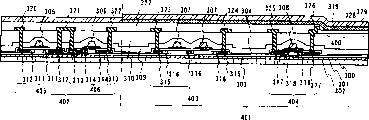
如图16A到16G所示,本发明的另一方面涉及一种制造半导体器件的方法,其中包括:在第一衬底10上形成要剥离的包括半导体元件的层13的第一步骤;利用第一粘合构件14将第二衬底15粘合到要剥离的层13上,从而将这个要剥离的层夹在第一衬底和第二衬底之间的第二步骤;从要剥离的层13上分离第一衬底10的第三步骤;利用第二粘合构件16将其中形成了保护模18的第三衬底17粘合到剥离层上,从而将该剥离层夹在第二衬底和第三衬底之间的第四步骤;以及从该剥离层上分离第二衬底并从第二粘合构件上分离第三衬底以形成用第二粘合构件16和保护模18作支撑体的剥离层的第五步骤。As shown in FIGS. 16A to 16G, another aspect of the present invention relates to a method of manufacturing a semiconductor device, including: a first step of forming a
在上述结构中,制造方法的特征在于:保护模是氮化硅膜或氧氮化硅膜。通过形成保护膜,可以有效地阻止来自外界的湿气和杂质以避免污染。In the above structure, the manufacturing method is characterized in that the protective mold is a silicon nitride film or a silicon oxynitride film. By forming a protective film, moisture and impurities from the outside can be effectively blocked to avoid contamination.
附图说明Description of drawings
附图中:In the attached picture:
图1A到1G是显示实施模式1的工艺图;1A to 1G are process diagrams showing
图2A到2G是显示实施模式2的工艺图;2A to 2G are process diagrams showing Embodiment Mode 2;
图3A到3G是显示实施模式3的工艺图;3A to 3G are process diagrams showing
图4是具有元件的第一衬底的截面图;Figure 4 is a cross-sectional view of a first substrate with elements;
图5是具有OLED的发光器件的截面图;5 is a cross-sectional view of a light emitting device having an OLED;
图6A和6B分别是具有OLED的发光器件的顶视图及其截面图;6A and 6B are a top view and a cross-sectional view thereof, respectively, of a light emitting device having an OLED;
图7是具有OLED的发光器件的截面图;7 is a cross-sectional view of a light emitting device having an OLED;
图8是有源矩阵液晶显示器件的截面图;8 is a cross-sectional view of an active matrix liquid crystal display device;
图9是显示剥离之前n沟道TFT的V-I特性的曲线图;FIG. 9 is a graph showing V-I characteristics of an n-channel TFT before lift-off;
图10是显示剥离之前p沟道TFT的V-I特性的曲线图;FIG. 10 is a graph showing V-I characteristics of a p-channel TFT before lift-off;
图11是显示剥离之后n沟道TFT的V-I特性的曲线图;11 is a graph showing V-I characteristics of an n-channel TFT after lift-off;
图12是显示剥离之前p沟道TFT的V-I特性的曲线图;12 is a graph showing V-I characteristics of a p-channel TFT before lift-off;
图13A到13F是显示电子设备的示例的简图;13A to 13F are diagrams showing examples of electronic equipment;
图14是显示电子设备的示例的简图;14 is a diagram showing an example of an electronic device;
图15A到15C是显示电子设备的示例的简图;15A to 15C are diagrams showing examples of electronic equipment;
图16A到16G是显示本发明的工艺图示例;16A to 16G are examples of process drawings showing the present invention;
图17是示出显示板的外形图的照片;FIG. 17 is a photograph showing an outline view of a display panel;
图18是示出发光的显示板的照片。Fig. 18 is a photograph showing a display panel emitting light.
具体实施方式Detailed ways
下面将对本发明的实施模式进行描述。Embodiment modes of the present invention will be described below.
[实施模式1][Implementation Mode 1]
以下是对利用本发明的典型剥离过程以及半导体器件制造方法的简述。描述将参考图1A到1G。The following is a brief description of a typical lift-off process and method of manufacturing a semiconductor device utilizing the present invention. The description will refer to FIGS. 1A to 1G .
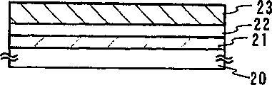
在图1A中,标号10表示第一衬底,11表示氮化层或金属层的第一材料层,12表示氧化层的第二材料层,以及13表示要剥离的层。In FIG. 1A,
图1A中的第一衬底10可以是玻璃衬底、石英衬底、陶瓷衬底等。也可以使用一般为硅衬底的半导体衬底或一般为不锈钢衬底的金属衬底。The
首先,在衬底10上形成第一材料层11,如图1A所示。第一材料层11一旦形成就可能具有压缩应力或张应力。但是,重要的是将这样的材料用于第一材料层11:它不受由用于形成要剥离的层的热处理或激光照射引起的剥离或其它干扰的影响、并且在要剥离的层形成之后该层具有1到1×10¹⁰dyne/cm2(达因/平方厘米)的张应力。其典型示例是从由W、WN、TiN和TiW组成的组中选择的成分的单层、或者主要包含上述成分的合金材料或化合物材料的单层、或者上述成分的叠层结构。通过溅射形成第一材料层11。First, a
接下来,在第一材料层11上形成第二材料层12。重要的是将这样的材料用于第二材料层12:它不受由用来形成要剥离的层的热处理或激光照射引起的剥离或其它干扰的影响、并且在要剥离的层形成之后该层具有1到1×10¹⁰dyne/cm2的张应力。第二材料层12的典型示例是氧化硅、氮氧化硅和金属氧化物的单层或叠层结构。可以通过溅射形成第二材料层12。在通过溅射形成第二材料层12时,一般为氩气的惰性气体被引进到反应室中、使得在第二材料层12中包含极少量的惰性成分。Next, the
第一材料层11和第二材料层12被分别设置为具有范围在1nm(纳米)和100nm之间的适当厚度,以便调整第一材料层11的内应力和第二材料层12的内应力。The
图1A到1G显示了一个示例,其中形成的第一材料层11与衬底10接触以便简化工艺。但是,可以在衬底10和第一材料层11之间形成用作缓冲层的绝缘层或金属层,以便改善第一材料层11到衬底10的粘合力。1A to 1G show an example in which a
接着,在第二材料层12上形成要剥离的层13(图1A)。要剥离的层13是包含各种元件(薄膜晶体管、具有OLED的发光元件、液晶元件、存储元件、薄膜二极管、硅的PIN结的光电转换元件、硅电阻元件)的层。当所述元件是具有液晶的元件时,要剥离的层13包括对面的衬底。要剥离的层13可以通过在第一衬底10能够耐受的温度下的热处理来形成。在本发明中,并非通过用于形成要剥离的层13的热处理来剥离薄膜,尽管第二材料层12的内应力不同于第一材料层11的内应力。Next, the
下述工艺用于部分降低第一材料层11和第二材料层12之间的粘合力。用于部分降低粘合力的处理是激光照射,其中用光沿着要剥离区域的周边部分照射第二材料层或第一材料层,或沿着要剥离区域的周边从外部施加的局部压力、以损坏第二材料层内部的一部分或界面的一部分。具体地说,用金刚石笔等垂直压下硬针、并且边移动所述层边施加负荷。最好使用划线器装置并且将下压量设在0.1到2mm,以便边移动所述层边施加压力。以这种方式在剥离之前提供促进剥离现象的部分、即引发机制是重要的。由于选择性(部分地)降低粘合力的预处理,避免了剥离失败并且提高了产量。The following process is used to partially reduce the adhesive force between the
接下来,利用第一粘合构件14将第二衬底15粘合到要剥离的层13(图1B)。反应固化粘合剂、热固化粘合剂、诸如UV固化粘合剂的光固化粘合剂、厌氧粘合剂和其它各种类型的固化粘合剂可以被用作第一粘合构件14。这些粘合剂可溶于溶剂或者可以是光敏的且在用光照射时粘合力降低。这些粘合剂可具有任何成分并且可以是例如基于环氧树脂的、基于丙烯酸酯的或基于硅酮的。例如通过涂敷将粘合剂制成粘合构件。在后续步骤中去除第一粘合构件。这里,将可溶于溶剂的粘合剂材料选作第一粘合构件。Next, the
第二衬底15可以是玻璃衬底、石英衬底、陶瓷衬底、塑料衬底等。也可以使用一般为硅衬底的半导体衬底或一般为不锈钢衬底的金属衬底。偶尔在光敏粘合构件被用作第一粘合构件或第二粘合构件的情况下,作为第一衬底和第二衬底之一,最好使用具有透光的衬底。The
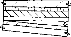
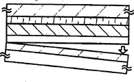
接下来,将其上形成了第一材料层11的第一衬底10按图1C中箭头所示的方向、用物理方法从部分降低了粘合力的区域的那一侧开始(图1C)撕开。由于第二材料层12具有压缩应力而第一材料层11具有张应力,因此可用相对小的力(如用手、通过喷嘴喷射的气压、超声波等)撕开第一衬底。Next, the
在第一材料层12上形成的要剥离的层13可以用这种方式从第一衬底10上分离。图1D中显示了剥离后的状态。The layer to be peeled off 13 formed on the
随后,利用由不同于第一粘合构件14的材料构成的第二粘合构件16将第三衬底17粘合到第二材料层12(和剥离层13)。重要的是第二粘合构件16到第二材料层12(和剥离层13)的粘合力大于它到第三衬底17的粘合力。Subsequently, the third substrate 17 is bonded to the second material layer 12 (and the release layer 13 ) with the
反应固化粘合剂、热固化粘合剂、诸如UV固化粘合剂的光固化粘合剂、厌氧粘合剂和其它各种类型的固化粘合剂可以被用作第二粘合构件16。这些粘合剂可溶于溶剂或者可以是光敏的因而粘合力在用光照射时降低。这些粘合剂可以具有任何成分并且可以是基于环氧树脂的、基于丙烯酸酯的或基于硅酮的。例如通过涂敷将粘合剂制成粘合构件。第二粘合构件在后续步骤中成为剥离层的支撑体。这里,UV固化粘合剂被用作第二粘合构件16。Reaction curing adhesives, heat curing adhesives, light curing adhesives such as UV curing adhesives, anaerobic adhesives, and other various types of curing adhesives may be used as the
第三衬底17可以是玻璃衬底、石英衬底、陶瓷衬底、塑料衬底等。也可以使用一般为硅衬底的半导体衬底或一般为不锈钢衬底的金属衬底。这里,为了降低第二粘合材料到第三衬底的粘合力,在其表面上形成了AlNXOY膜的塑料膜被用作第三衬底17。The third substrate 17 may be a glass substrate, a quartz substrate, a ceramic substrate, a plastic substrate, or the like. A semiconductor substrate, generally a silicon substrate, or a metal substrate, generally a stainless steel substrate may also be used. Here, in order to reduce the adhesive force of the second adhesive material to the third substrate, a plastic film having an AlNxOY film formed on its surface was used as the third substrate 17 .
利用例如氮化铝(AlN)靶在通过将氩气、氮气和氧气混合得到的气氛中进行溅射在塑料膜上形成AlNXOY膜。AlNXOY膜包括几个或更多氮气压百分比就足够了,最好为2.5到47.5氮气压百分比(atm%)。可以通过调整溅射条件来按需调整氮浓度(衬底温度、原料气的类型和流速、成膜压力等)。 An AlNxOY film is formed on the plastic film by sputtering using, for example, an aluminum nitride (AlN) target in an atmosphere obtained by mixing argon, nitrogen, and oxygen. It is sufficient that the AlN X O Y film includes several or more nitrogen gas pressure percentages, preferably 2.5 to 47.5 nitrogen gas pressure percentages (atm%). Nitrogen concentration can be adjusted as needed by adjusting sputtering conditions (substrate temperature, type and flow rate of raw material gas, film forming pressure, etc.).
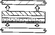
接下来,将所述各层浸入溶剂中以便分离第二衬底15和第三衬底17(图1F)。第一粘合构件易于被去除,因为它是由可溶于溶剂中的粘合剂材料构成的,从而将第二衬底15从剥离层13上分离。另一方面,溶剂渗透第三衬底17和第二粘合构件16之间的界面并减弱了界面处的粘合力,从而将第三衬底17从第二材料层12上分离。尽管在这里所示的示例中在同一步骤中分离第二衬底15和第三衬底17,但并不存在特定限制。这些衬底可以在不同步骤中分离并且首先分离它们中的哪一个并不固定。Next, the layers are immersed in a solvent to separate the
这样形成剥离层13中包括的元件、使得其输入/输出端暴露在剥离层的最上层(即最靠近第二衬底侧的层)。因此,需要在分离第二衬底的步骤完成之后再去除剥离层上的第一粘合构件,从而暴露输入/输出端。The elements included in the
通过上述步骤制造具有剥离层13的半导体器件,其中第二粘合构件16被用作支撑体(图1g)。这样得到的半导体器件即薄且轻,并且具有柔性,因为支撑体只由第二粘合构件16构成。A semiconductor device having a
在这里示意的示例中,通过上述步骤来完成半导体器件。上述步骤可被用于部分地完成半导体器件。例如,元件形成步骤可被添加到上述步骤中、以便在上述步骤之后形成包括TFT的电路的剥离层进而可在元件形成步骤中利用所获得的用第二粘合构件作支撑体的剥离层,以完成各种不同类型的半导体器件,一般为具有OLED的发光器件或液晶显示器件。In the example illustrated here, a semiconductor device is completed through the above steps. The above-described steps can be used to partially complete a semiconductor device. For example, an element forming step may be added to the above steps so that a release layer of a circuit including TFTs is formed after the above steps and the obtained release layer using the second adhesive member as a support can be utilized in the element forming step, To complete various types of semiconductor devices, generally light-emitting devices with OLEDs or liquid crystal display devices.
例如,可以通过以下步骤来制造有源矩阵发光器件:配置像素电极以形成矩阵图案;通过上述步骤形成具有连接到像素电极的TFT的第二粘合构件;以及形成用像素电极作负极或正极的OLED。这样得到的发光器件即薄且轻,因为支撑体仅由第二粘合构件构成。For example, an active matrix light emitting device can be manufactured through the steps of: disposing pixel electrodes to form a matrix pattern; forming a second adhesive member having TFTs connected to the pixel electrodes through the above steps; OLED. The light-emitting device thus obtained is thin and light since the support is composed of only the second adhesive member.
还可能制造具有OLED的无源发光器件。It is also possible to manufacture passive light emitting devices with OLEDs.
同样,可以通过以下步骤来制造有源矩阵液晶显示器:配置像素电极以形成矩阵图案;通过上述步骤形成具有连接到像素电极的TFT的第二粘合构件;之后是相对衬底粘贴步骤和液晶注入步骤。具体地说,密封构件等被用于将相对衬底粘贴到具有连接到像素电极的TFT的粘合构件,同时用诸如垫片的间隙保持构件在相对衬底和粘合构件支撑体之间保持一定的距离。接着在相对衬底和像素电极之间装入液晶材料以完成液晶显示器件。这样得到的液晶显示器件即薄且轻,因为支撑体仅由第二粘合构件和相对衬底构成。Also, an active matrix liquid crystal display can be manufactured through the following steps: configuring pixel electrodes to form a matrix pattern; forming a second adhesive member having TFTs connected to the pixel electrodes through the above steps; followed by an opposing substrate sticking step and liquid crystal injection step. Specifically, a sealing member or the like is used to stick the opposing substrate to the adhesive member having the TFT connected to the pixel electrode, while holding the gap between the opposing substrate and the adhesive member support with a gap maintaining member such as a spacer. a certain distance. Then a liquid crystal material is filled between the opposite substrate and the pixel electrodes to complete the liquid crystal display device. The liquid crystal display device thus obtained is thin and light since the support is constituted only of the second adhesive member and the opposing substrate.
[实施模式2][Implementation Mode 2]
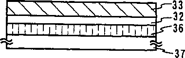
实施模式1显示了其中第二粘合构件单独用作支撑体的示例。在本实施模式中,显示了用第一粘合构件和第二粘合构件作支撑体的示例。图2A到图2E基本与图1A到1E相同。因此,这里将省略细节描述并且将只对实施模式1和实施模式2之间的不同之处进行描述。
在图2A到2G中,标号20表示第一衬底,21表示是氮化层或金属层的第二材料层,22表示是氧化层的第二材料层,23表示要剥离的层,24表示第二粘合构件,25表示第二衬底,26表示第二粘合构件以及27表示第三衬底。2A to 2G,
首先,根据第一实施模式1,以相同的程序得到图2E的状态。First, according to the
这里,反应固化粘合剂、热固化粘合剂、诸如UV固化粘合剂的光固化粘合剂、厌氧粘合剂和其它各种类型的固化粘合剂可以被用作第一粘合构件24。这些粘合剂可溶于溶剂或者可以是光敏的因而在用光照射时粘合力降低。这些粘合剂可以具有任何成分并且可以是基于环氧树脂的、基于丙烯酸酯的或基于硅酮的。例如通过涂敷而将粘合剂制成粘合构件。在后续步骤中第一粘合构件成为支撑体。这里,用紫外线照射时粘合力会降低的热固化粘合剂被用作第一粘合构件。重要的是第一粘合构件24到剥离层23的粘合力大于它到第二衬底25的粘合力。Here, reaction curing adhesives, heat curing adhesives, light curing adhesives such as UV curing adhesives, anaerobic adhesives, and other various types of curing adhesives can be used as the first adhesive.
为了降低第一粘合构件到第二衬底的粘合力,可将表面上形成了AlNXOY膜的塑料膜用作第二衬底。In order to reduce the adhesive force of the first adhesive member to the second substrate, a plastic film on which an AlNxOY film is formed may be used as the second substrate.
第二粘合构件26的材料可以与第一粘合构件24的材料相同。这里,粘合力在用紫外线照射时会降低的热固化粘合剂被用作第二粘合构件。第二粘合构件在后续步骤中也用作剥离层的支撑体。重要的是第二粘合构件26到第二材料层22(和剥离层23)的粘合力大于它到第三衬底27的粘合力。The material of the
为了降低第二粘合构件到第三衬底的粘合力,可将表面上形成了AlNXOY膜的塑料膜用作第三衬底。In order to reduce the adhesive force of the second adhesive member to the third substrate, a plastic film on which an AlNxOY film is formed may be used as the third substrate.
通过进行实施模式1的过程得到图2E的状态。接着用紫外线照射粘合构件,以降低第一粘合构件24到第二衬底25的粘合力以及第二粘合构件26到第三衬底27的粘合力,从而将第二衬底和第三衬底分离(图2F)。尽管在这里所示的示例中在同一步骤中分离第二衬底25和第三衬底27,但并不存在特定限制。这些衬底可以在不同步骤中分离并且首先分离它们中的哪一个并不固定。本实施模式还可以与实施模式1进行组合。The state of FIG. 2E is obtained by performing the process of implementing
尽管在这里所示的示例中使用了通过紫外线照射降低粘合力的热固化粘合剂,但也可以使用其它粘合剂材料。例如,UV固化粘合剂可被用作第一粘合构件和第二粘合构件。在这种情况下,在其表面上形成了AlNXOY膜的塑料膜被用作第二衬底并通过由UV固化粘合剂构成的第一粘合构件粘合,在其表面上形成了AlNXOY膜的塑料膜被用作第三衬底并通过由UV固化粘合剂构成的第二粘合构件粘合。之后,这些层被浸入溶剂中并且溶剂渗透到第三衬底和第二粘合构件之间的界面,从而将第二材料层与第三衬底分离。类似地将第一粘合构件与第二衬底分离。Although in the example shown here a thermally cured adhesive that is reduced in adhesion by ultraviolet radiation is used, other adhesive materials may also be used. For example, a UV-curable adhesive may be used as the first adhesive member and the second adhesive member. In this case, a plastic film having an AlN X O Y film formed on its surface is used as a second substrate and bonded by a first bonding member composed of a UV-curable adhesive, forming on its surface A plastic film containing an AlNxOY film was used as a third substrate and bonded by a second bonding member composed of a UV-curable adhesive. Thereafter, the layers are immersed in a solvent and the solvent penetrates into the interface between the third substrate and the second bonding member, thereby separating the second material layer from the third substrate. The first bonding member is similarly separated from the second substrate.
这样形成包括在剥离层23中的元件、使得其输入/输出端暴露在剥离层的最上层(即最靠近第二衬底侧的层)。因此,需要选择性地在分离第二衬底的步骤之后去除覆盖输入/输出端部分的第一粘合构件,从而暴露输入/输出端部分。The elements included in the
通过图2G中显示的上述步骤制造了具有剥离层23的半导体器件,其中第一粘合构件24和第二粘合构件26用作支撑体。注意,剥离层23被夹在第一粘合构件24和第二粘合构件26之间。这样得到的半导体器件既薄且轻,并且具有柔性,因为支撑体仅由第一粘合构件24和第二粘合构件26构成。A semiconductor device having a
在这里显示的示例中,通过上述步骤完成半导体器件。上述步骤可被用于部分地完成半导体器件。例如,可以将元件形成步骤添加到上述步骤中,以便按照上述步骤形成包括包含TFT的电路的剥离层,并且这样形成的将第一粘合构件和第二粘合构件作为支撑体的剥离层可被用于元件形成步骤中,以完成各种不同类型的半导体器件,一般为具有OLED的发光器件或液晶显示器件。In the example shown here, a semiconductor device is completed through the above steps. The above-described steps can be used to partially complete a semiconductor device. For example, an element forming step may be added to the above-mentioned steps so that a peeling layer including a circuit including TFTs is formed according to the above-mentioned steps, and the thus-formed peeling layer having the first adhesive member and the second adhesive member as a support can be Used in element forming steps to complete various types of semiconductor devices, generally light emitting devices with OLEDs or liquid crystal display devices.
本实施模式可以与实施模式1自由组合。This implementation mode can be freely combined with
[实施模式3][Implementation Mode 3]
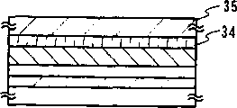
实施模式1显示了其中第二粘合构件单独用作支撑体的示例。在本实施模式中,显示了用第二粘合构件和第三衬底作支撑体的示例。图3A到3E基本与图1A到1E相同。所以这里将省略细节描述,并且将只对实施模式1和实施模式3之间的不同之处进行描述。
在图3A到3G中,标号30表示第一衬底,31表示是氮化层或金属层的第一材料层,32表示是氧化层的第二材料层,33表示要剥离的层,34表示第一粘合构件,35表示第二衬底,36表示第二粘合构件以及37表示第三衬底。3A to 3G,
首先,根据实施模式1,以相同的过程得到图3E的状态。First, according to the
第一衬底30可以是玻璃衬底、石英衬底、陶瓷衬底等。还可以使用一般为硅衬底的半导体衬底或一般为不锈钢衬底的金属衬底。这里使用厚度为0.7mm的玻璃衬底(#1737)。The
这里,把比第一衬底30更厚和更高硬度的石英衬底(厚度1.1mm)用作第二衬底35。如果用塑料膜作第二衬底,则当在第一衬底上形成的元件被转移到塑料膜上时,换句话说,当利用第一粘合构件34将剥离层33粘合到该膜上并且该膜被提起时,担心膜会弯曲并且剥离层33可能因为弯曲导致断裂。因此,通过以下工序降低断裂的可能性:利用第一粘合构件34将在第一衬底30上形成的剥离层33粘贴到非常硬的第二衬底35上;剥离第一衬底30;利用第二粘合构件36将塑料膜(第三衬底37)粘贴到包括元件的层上;然后分离第二衬底35。Here, a quartz substrate (1.1 mm in thickness) thicker and higher in hardness than the
这里的第三衬底37是塑料膜。The
这里,挑选溶于溶剂的粘合剂材料用作第一粘合构件34。Here, a solvent-soluble adhesive material is selected for the first
这里用作第二粘合构件36的材料对第三衬底和剥离层都是高粘合力的。The material used here as the
遵照实施模式1的程序得到图3E的状态。然后,将这些层浸入溶剂中以单独分离第二衬底35(图3F)。由溶于溶剂的粘合剂材料构成的第一粘合构件易于被去除,从而从剥离层33上分离第二衬底35。The state of Fig. 3E is obtained by following the procedure of implementing
这样形成包含在剥离层33中的元件、使得其输入/输出端暴露在剥离层的最上层(即最靠近第二衬底侧的层)。因此,需要在分离第二衬底的步骤完成之后去除剥离层表面上的第一粘合构件,以便暴露输入/输出端部分。The elements contained in the
在这里显示的示例中,第一粘合构件34由一种溶于溶剂的粘合剂构成,并且将其浸入溶剂中以分离第二衬底。但是,不存在特殊限制,例如,可以通过用紫外线照射由热固化粘合剂(在紫外线照射下其粘合力降低)构成的第一粘合构件来分离第二衬底,如实施模式2所示。In the example shown here, the first
通过如图3G中显示的上述步骤制造了具有剥离层33的半导体器件,其中第二粘合构件36和第三衬底37用作支撑体。作为第二材料层的氧化层被插入在第二粘合构件36和剥离层33之间。这样得到的半导体器件整体上是柔性的,因为通过溅射形成第二材料层32并且第二材料层32中包括极少量的惰性气体成分。A semiconductor device having a
在这里显示的示例中,通过上述步骤完成半导体器件。上述步骤可被用于部分地完成半导体器件。例如,可以将元件形成步骤添加到上述步骤中,从而按照上述步骤形成包括包含TFT的电路的剥离层,并且这样获得的将第二粘合构件和第三衬底用作支撑体的剥离层可被用于元件形成步骤中,以完成各种不同类型的半导体器件,一般为具有OLED的发光器件或液晶显示器件。In the example shown here, a semiconductor device is completed through the above steps. The above-described steps can be used to partially complete a semiconductor device. For example, an element forming step may be added to the above-mentioned steps so that a peeling layer including a circuit including a TFT is formed according to the above-mentioned steps, and the thus obtained peeling layer using the second adhesive member and the third substrate as a support can be Used in element forming steps to complete various types of semiconductor devices, generally light emitting devices with OLEDs or liquid crystal display devices.
本实施模式可以与实施模式1或实施模式2自由组合。This implementation mode can be freely combined with
将通过以下实施例对上述结构的本发明进行更详细的描述。The present invention having the above structure will be described in more detail through the following examples.
[实施例1][Example 1]
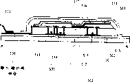
这里,将对制造具有OLED的发光器件的方法进行详细描述,其中同时在同一衬底上形成像素部分(n沟道TFT和p沟道TFT)和在像素部件的周围配置的驱动电路的TFT(n沟道TFT和p沟道TFT)(图4)。Here, a detailed description will be given of a method of manufacturing a light emitting device having an OLED in which a pixel portion (n-channel TFT and p-channel TFT) and TFTs of a driver circuit arranged around the pixel portion ( n-channel TFT and p-channel TFT) (Figure 4).
首先,通过等离子CVD在厚度为0.7mm的耐热玻璃衬底(第一衬底101)上形成厚度为100nm的氧氮化硅膜(未示出)。氧氮化硅膜用于保护衬底不受后续的干蚀刻影响并用于防止蚀刻室的污染,并且不是特别必需的。First, a silicon oxynitride film (not shown) with a thickness of 100 nm was formed on a heat-resistant glass substrate (first substrate 101 ) with a thickness of 0.7 mm by plasma CVD. The silicon oxynitride film is used to protect the substrate from subsequent dry etching and to prevent contamination of the etching chamber, and is not particularly necessary.
尽管在本实施例中将玻璃衬底用作第一衬底101,但不存在特定限制并且它可以是石英衬底、半导体衬底、陶瓷衬底或金属衬底。Although a glass substrate is used as the
接着,通过溅射在氧氮化硅膜上形成厚度为50nm的钨膜,作为第一材料层102。通过溅射形成的钨膜在衬底周边的厚度波动。因此,通过单独形成用于衬底周边的干蚀刻的抗蚀剂来形成钨膜图案。尽管这里形成了图案,但它并非特别必须的。第一材料层102并非限定于钨膜,也可使用其它材料,例如氮化钨或氮化钛。第一材料层102的厚度可以按需设置在10到200nm的范围内。Next, a tungsten film with a thickness of 50 nm was formed as the
在钨膜上通过溅射形成厚度为200nm的氧化硅膜,作为第二材料层103。尽管这里使用通过溅射形成的氧化硅膜,但也可以使用其它材料,例如氧化物,作为替代。第二材料层103的厚度可以按需设置在50到400nm的范围内。象这样在第一衬底上形成第一材料层102(钨膜)和第二材料层103(氧化硅膜),在后续步骤中在第二材料层上形成元件,然后施加机械力,以便在界面上将第一材料层和第二材料层彼此分离。最好在形成第二材料层103期间通过溅射形成诸如氩气的惰性气体流,以便在第二材料层103中包含极少量的惰性气体成分。A silicon oxide film with a thickness of 200 nm was formed as the
接着,通过在400℃温度下的等离子CVD利用SiH4、NH3和N2O作原料气在氧化硅膜上形成氧氮化硅膜(氧氮化硅膜的成分比例为:Si=32%,O=27%,N=24%,H=17%),作为基底绝缘膜的下层。氧氮化硅膜的厚度为50nm(最好为10到200nm)。膜表面用臭氧水清洗,然后用稀释的氟酸(稀释到1/100)去除表面上的氧化膜。接下来,通过在400℃温度下的等离子CVD利用SiH4和N2O作原料气形成氧氮化硅膜(氧氮化硅膜的成分比例为:Si=32%,O=59%,N=7%,H=2%),作为基底绝缘膜的上层。氧氮化硅膜的厚度为100nm(最好为50到200nm)并且覆盖在下层之上,以形成层叠结构。没有将所述层叠结构暴露于空气之中,通过在300℃温度下的等离子CVD利用SiH4作原料气在所述层叠结构上形成具有非晶态结构的半导体膜(这里为非晶硅膜)。半导体膜的厚度为54nm(最好为25到80nm)。Next, a silicon oxynitride film was formed on the silicon oxide film by plasma CVD at a temperature of 400° C. using SiH 4 , NH 3 and N 2 O as raw material gases (the composition ratio of the silicon oxynitride film is: Si=32% , O=27%, N=24%, H=17%) as the lower layer of the base insulating film. The thickness of the silicon oxynitride film is 50 nm (preferably 10 to 200 nm). The membrane surface was cleaned with ozone water, and then the oxide film on the surface was removed with diluted hydrofluoric acid (diluted to 1/100). Next, a silicon oxynitride film is formed by plasma CVD at a temperature of 400° C. using SiH 4 and N 2 O as raw material gases (the composition ratio of the silicon oxynitride film is: Si=32%, O=59%, N =7%, H=2%), as the upper layer of the base insulating film. The silicon oxynitride film has a thickness of 100 nm (preferably 50 to 200 nm) and overlies the lower layer to form a laminated structure. Without exposing the laminated structure to the air, a semiconductor film (here, an amorphous silicon film) having an amorphous structure was formed on the laminated structure by plasma CVD at a temperature of 300° C. using SiH 4 as a source gas. . The thickness of the semiconductor film is 54 nm (preferably 25 to 80 nm).
本实施例中的基底绝缘膜104具有两层结构。但是,基底绝缘膜可以是主要包含硅的单层或多于两层的绝缘膜。半导体膜的材料没有限制,但最好是通过已知方法(溅射、LPCVD、等离子CVD等)由硅或硅锗合金(SiXGe1-X(X=0.0001到0.02))构成的半导体膜。所用的等离子CVD装置可以是逐晶片进行处理的装置或成批处理的装置。可在同一室中连续形成基底绝缘膜和半导体膜,以避免与空气接触。The base
清洗具有非晶态结构的半导体膜的表面,然后利用臭氧水在该表面上形成大约2nm厚的非常薄的氧化膜。接着,用极少量的杂质成分(硼或磷)对半导体膜掺杂,以控制TFT的阈值。这里,通过离子掺杂的方法用硼对非晶硅膜进行掺杂,其中在没有质量分离的情况下利用等离子激发乙硼烷(B2H6)。掺杂条件包括将加速电压设置到15kV,通过用氢将乙硼烷稀释到1%得到30sccm的气体流速,而用量为2×10¹²/cm2。The surface of the semiconductor film having an amorphous structure is cleaned, and then a very thin oxide film of about 2 nm thick is formed on the surface with ozone water. Next, the semiconductor film is doped with a very small amount of impurity components (boron or phosphorus) to control the threshold of the TFT. Here, the amorphous silicon film is doped with boron by an ion doping method in which diborane (B 2 H 6 ) is excited with plasma without mass separation. The doping conditions included setting the acceleration voltage to 15 kV, a gas flow rate of 30 sccm obtained by diluting diborane to 1% with hydrogen, and an amount of 2×10 12 /cm 2 .
接下来,利用旋涂器涂敷包含按重量计为10ppm的镍的乙酸镍溶剂。镍可通过溅射而不是涂敷喷涂到整个表面。Next, a nickel acetate solvent containing 10 ppm by weight of nickel was applied using a spinner. Nickel can be sprayed over the entire surface by sputtering rather than coating.
半导体膜经过热处理而结晶并得到具有晶体结构的半导体膜。在电炉或利用强光照射来实现热处理。当采用电炉中的热处理时,温度被设置为500到650℃,并且处理持续4到24小时。这里,在热处理去氢(500℃下持续1小时)之后通过热处理进行晶化(550℃下持续4小时)得到具有晶体结构的硅膜。尽管这里利用电炉通过热处理晶化半导体膜,但也可以通过能够在短时间内实现晶化的退火装置进行晶化。本实施例采用了一种晶化技术,其中镍被用作加速硅的晶化的金属成分。但也可以采用其它已知的诸如固相生长和激光晶化的晶化技术。The semiconductor film is crystallized by heat treatment and a semiconductor film having a crystal structure is obtained. Heat treatment is achieved in an electric furnace or by irradiation with strong light. When heat treatment in an electric furnace is employed, the temperature is set at 500 to 650° C., and the treatment lasts for 4 to 24 hours. Here, crystallization was performed by heat treatment (550° C. for 4 hours) after dehydrogenation by heat treatment (500° C. for 1 hour) to obtain a silicon film having a crystal structure. Although here the semiconductor film is crystallized by heat treatment using an electric furnace, it may also be crystallized by an annealing apparatus capable of achieving crystallization in a short time. The present embodiment employs a crystallization technique in which nickel is used as a metal component to accelerate crystallization of silicon. However, other known crystallization techniques such as solid phase growth and laser crystallization may also be used.
通过稀释的氟酸等去除具有晶体结构的硅膜表面上的氧化膜。然后,为了提高晶化速度并修正晶粒中存留的缺陷,在空气中或氧气环境中用激光(波长为308nm的XeCl)照射硅膜。激光可以是波长为400nm或更短的准分子激光,或者可以是YAG激光器的二次谐波或三次谐波。采用具有重复频率为10到1000Hz的脉冲激光。由光学系统聚集激光,以便具有100到400mJ/cm2的能量密度,并以90%到95%的重叠比率扫描硅膜表面。这里,在空气中用重复频率为30Hz、能量密度为470mJ/cm2的激光照射所述膜。由于是在空气或氧气环境中进行激光照射的,因此在表面上形成了氧化膜。这里显示的示例中使用了脉冲激光器,但也可以采用连续波激光器。最好采用连续波固态激光器以及基波的二次到四次谐波,以便在对非晶体半导体膜进行晶化时得到大粒度晶体。一般采用Nd∶YVO4激光器(基波:1064nm)的二次谐波(532nm)和三次谐波(355nm)。当利用连续波激光器时,从10W功率连续波YVO4激光器发出的激光被非线性光学部件转换成谐波。或者,通过将YVO4晶体和非线性光学部件设置在谐振器中得到谐波。谐波最好由光学系统成形为照射表面上的长方形或椭圆形的激光,然后对照射对象进行照射。这时所需的能量密度大约为0.01到100MW/cm2。(最好为0.1到10MW/cm2)。照射期间,半导体膜以10到2000cm/s的速度相对于激光移动。The oxide film on the surface of the silicon film having a crystal structure is removed by diluted hydrofluoric acid or the like. Then, in order to increase the crystallization rate and correct defects remaining in the crystal grains, the silicon film is irradiated with laser light (XeCl with a wavelength of 308 nm) in air or in an oxygen atmosphere. The laser may be an excimer laser with a wavelength of 400 nm or less, or may be the second or third harmonic of a YAG laser. A pulsed laser with a repetition rate of 10 to 1000 Hz is used. Laser light is condensed by an optical system so as to have an energy density of 100 to 400 mJ/cm 2 , and the surface of the silicon film is scanned at an overlap ratio of 90% to 95%. Here, the film was irradiated with laser light at a repetition frequency of 30 Hz and an energy density of 470 mJ/cm 2 in air. Since laser irradiation is performed in an air or oxygen atmosphere, an oxide film is formed on the surface. The example shown here uses a pulsed laser, but continuous wave lasers can also be used. It is preferable to use a continuous wave solid-state laser and the second to fourth harmonics of the fundamental wave in order to obtain large-grained crystals when crystallizing an amorphous semiconductor film. The second harmonic (532nm) and third harmonic (355nm) of Nd:YVO 4 laser (fundamental wave: 1064nm) are generally used. When using a continuous wave laser, the laser light emitted from a 10W power continuous wave YVO 4 laser is converted into harmonics by nonlinear optics. Alternatively, harmonics can be obtained by placing a YVO 4 crystal and nonlinear optics in the resonator. The harmonics are preferably shaped by the optical system to illuminate a rectangular or elliptical laser light on the surface and then illuminate the illuminated object. The energy density required at this time is about 0.01 to 100 MW/cm 2 . (preferably 0.1 to 10 MW/cm 2 ). During irradiation, the semiconductor film moves relative to the laser light at a speed of 10 to 2000 cm/s.
用稀释的氟酸去除通过激光照射形成的氧化膜,然后用臭氧水处理该表面120秒,以形成总厚度为1到5nm的氧化膜作为阻挡层。这里利用臭氧水形成阻挡层,但也可以通过在氧气环境中通过紫外线照射氧化具有晶体结构的半导体膜的表面来形成,或通过氧等离子体处理氧化具有晶体结构的半导体膜的表面来形成,或通过利用等离子CVD、溅射或蒸发形成大约1到10nm厚的氧化膜。在本说明书中,阻挡层指的是这样的层:它具有允许金属成分在吸气步骤中通过的质量和厚度并在去除作为吸气点的层的步骤中作为蚀刻终止层。The oxide film formed by laser irradiation was removed with diluted hydrofluoric acid, and then the surface was treated with ozone water for 120 seconds to form an oxide film with a total thickness of 1 to 5 nm as a barrier layer. Here, ozone water is used to form the barrier layer, but it can also be formed by oxidizing the surface of the semiconductor film having the crystal structure by ultraviolet irradiation in an oxygen atmosphere, or by oxidizing the surface of the semiconductor film having the crystal structure by oxygen plasma treatment, or An oxide film of about 1 to 10 nm thick is formed by using plasma CVD, sputtering or evaporation. In this specification, the barrier layer refers to a layer which has a mass and thickness to allow metal components to pass through in a gettering step and serves as an etching stopper in a step of removing a layer serving as a gettering point.
接下来,通过溅射在阻挡层上形成包含氩的非晶硅膜,用作吸气点,非晶硅膜的厚度为50到400nm,这里为150nm。这里形成非晶硅膜的条件包括将成膜压力设置为0.3Pa,气体(Ar)流速为50sccm,成膜功率为3kW,以及衬底温度为150℃。在上述条件下形成的非晶硅膜中所包含的氩的原子浓度为3×10²⁰到6×10²⁰/cm3并且其中的氧的原子浓度为1×1019到3×1019/cm3。之后,在550℃电炉中进行4小时的热处理用于吸气,以减少具有晶体结构的半导体膜中的镍浓度。可以使用灯退火装置代替电炉。Next, an amorphous silicon film containing argon serving as a gettering point is formed on the barrier layer by sputtering to a thickness of 50 to 400 nm, here 150 nm. The conditions for forming the amorphous silicon film here include setting the film forming pressure at 0.3 Pa, the gas (Ar) flow rate at 50 sccm, the film forming power at 3 kW, and the substrate temperature at 150°C. The atomic concentration of argon contained in the amorphous silicon film formed under the above conditions is 3×10 20 to 6×10 20 /cm 3 and the atomic concentration of oxygen therein is 1×10 19 to 3×10 19 /cm 3 . After that, heat treatment for gettering was performed in an electric furnace at 550° C. for 4 hours to reduce the nickel concentration in the semiconductor film having a crystal structure. A lamp annealing device can be used instead of an electric furnace.
利用阻挡层作为蚀刻终止层,选择性地去除吸气点、即包含氩的非晶硅膜。然后,通过稀释的氟酸选择性地去除阻挡层。镍在吸气期间倾向于向具有高氧浓度的区域移动,因而需要在吸气后去除成为氧化膜的阻挡层。Using the stopper layer as an etching stopper, the getter points, that is, the amorphous silicon film containing argon, are selectively removed. Then, the barrier layer is selectively removed by dilute hydrofluoric acid. Nickel tends to move to a region with a high oxygen concentration during gettering, so it is necessary to remove the barrier layer which becomes an oxide film after gettering.
接下来,利用臭氧水在得到的包含晶体结构的硅膜(也被称为多晶硅膜)的表面上形成薄氧化层。然后形成抗蚀剂掩膜并且对硅膜进行蚀刻以形成彼此分离的岛状半导体层并具有所需形状。形成半导体层之后去除抗蚀剂掩膜。Next, a thin oxide layer is formed on the surface of the resulting silicon film containing a crystal structure (also referred to as a polysilicon film) using ozone water. A resist mask is then formed and the silicon film is etched to form island-shaped semiconductor layers separated from each other and have a desired shape. The resist mask is removed after the semiconductor layer is formed.
用包含氟酸的蚀刻剂去除氧化膜,并且同时清洗硅膜表面。接着形成主要包含硅的绝缘膜用作栅绝缘膜105。这里的栅绝缘膜是通过等离子CVD形成的厚度为115nm的氧氮化硅膜(成分比例:Si=32%,O=59%,N=7%,H=2%)。The oxide film is removed with an etchant containing hydrofluoric acid, and at the same time, the surface of the silicon film is cleaned. Next, an insulating film mainly containing silicon is formed as the
接下来,在栅绝缘膜上形成厚度为20到100nm的第一导电膜和厚度为100到400nm的第二导电膜的叠层结构。在本实施例中,在栅绝缘膜105上形成厚度为50nm的氮化钽膜然后在其上覆盖厚度为370nm的钨膜。按下述程序形成导电膜图案,以形成栅极和导线。Next, a laminated structure of a first conductive film having a thickness of 20 to 100 nm and a second conductive film having a thickness of 100 to 400 nm is formed on the gate insulating film. In this embodiment, a tantalum nitride film with a thickness of 50 nm is formed on the
第一导电膜和第二导电膜的导电材料是选自由Ta、W、Ti、Mo、Al和Cu、或者主要包含上述元素的合金或化合物组成的组中选择的成分。第一导电膜和第二导电膜可以是半导体膜,一般为多晶硅膜,其中用磷或其它杂质元素进行掺杂或者可以是Ag-Pd-Cu合金膜。本发明并不限于两层导电膜。例如,可以采用以下列顺序层叠的包括50nm厚的钨膜、500nm厚的铝硅合金(Al-Si)膜和30nm厚的氮化钛膜的三层结构。当采用三层结构时,可以用氮化钨代替第一导电膜的钨,用铝钛合金(Al-Ti)膜代替第二导电膜的铝硅合金(Al-Si)膜,以及用钛膜代替第三导电膜的氮化钛膜。或者,可以使用单层导电膜。The conductive material of the first conductive film and the second conductive film is a component selected from the group consisting of Ta, W, Ti, Mo, Al, and Cu, or alloys or compounds mainly containing the above elements. The first conductive film and the second conductive film may be semiconductor films, generally polysilicon films, which are doped with phosphorus or other impurity elements or may be Ag-Pd-Cu alloy films. The present invention is not limited to two conductive films. For example, a three-layer structure including a 50 nm-thick tungsten film, a 500 nm-thick aluminum-silicon alloy (Al-Si) film, and a 30 nm-thick titanium nitride film laminated in the following order may be employed. When a three-layer structure is adopted, the tungsten of the first conductive film can be replaced by tungsten nitride, the aluminum-silicon alloy (Al-Si) film of the second conductive film can be replaced by an aluminum-titanium alloy (Al-Ti) film, and the titanium film can be replaced by a titanium film. A titanium nitride film instead of the third conductive film. Alternatively, a single-layer conductive film may be used.
最好将ICP(感应耦合等离子体)蚀刻用于第一导电膜和第二导电膜的蚀刻(第一蚀刻处理和第二蚀刻处理)。通过利用ICP蚀刻并调整蚀刻条件(加到线圈电极的电功率量、加到衬底侧电极的电功率量、衬底侧电极的温度等),可以按需蚀刻并使膜成锥形。在形成了抗蚀剂掩膜之后进行第一蚀刻处理。第一蚀刻条件包括在1Pa(帕斯卡)压强下对线圈电极施加700W的RF(13.56MHz)功率,采用CF4、Cl2和O2作为蚀刻气体,以及设置其中的气体流速比例为25∶25∶10(sccm)。衬底侧(样本阶段)还接收150W(13.56MHz)的RF功率,以提供基本上为负的自偏压。衬底侧电极的面积(大小)为12.5cm×12.5cm,并且线圈电极是直径25cm的盘(这里是在其上设置线圈的石英盘)。在这些第一蚀刻条件下蚀刻W膜,从而在边缘周围形成锥形。之后,从第一蚀刻条件切换到第二蚀刻条件,并不去除抗蚀剂掩膜。第二蚀刻条件包括采用CF4和Cl2作为蚀刻气体,设置其中的气体流速比例为30∶30(sccm),并在1Pa压强下对线圈电极施加500W的RF(13.56MHz)功率,以产生等离子体进行约30分钟的蚀刻。衬底侧(样本阶段)还接收20W(13.56MHz)的RF功率,以提供基本上为负的自偏压。在使用CF4和Cl2的混合的第二蚀刻条件下,W膜和TaN膜被蚀刻到几乎相同的程度。所述第一蚀刻条件和第二蚀刻条件构成第一蚀刻处理。ICP (Inductively Coupled Plasma) etching is preferably used for the etching of the first conductive film and the second conductive film (first etching treatment and second etching treatment). By etching using ICP and adjusting etching conditions (amount of electric power applied to the coil electrode, amount of electric power applied to the substrate-side electrode, temperature of the substrate-side electrode, etc.), the film can be etched and tapered as desired. The first etching process is performed after the resist mask is formed. The first etching condition comprises applying RF (13.56MHz) power of 700W to the coil electrode under 1Pa (Pascal) pressure, adopting CF 4 , Cl 2 and O 2 as etching gases, and setting the ratio of gas flow rates therein to 25:25: 10 (sccm). The substrate side (sample stage) also received 150W (13.56MHz) of RF power to provide a substantially negative self-bias. The area (size) of the substrate-side electrode was 12.5 cm×12.5 cm, and the coil electrode was a disk (here, a quartz disk on which a coil was provided) with a diameter of 25 cm. The W film is etched under these first etching conditions to form a taper around the edge. Thereafter, switching from the first etching condition to the second etching condition does not remove the resist mask. The second etching condition includes adopting CF 4 and Cl 2 as etching gas, setting the ratio of gas flow rate therein to 30:30 (sccm), and applying 500W of RF (13.56MHz) power to the coil electrode under 1Pa pressure to generate plasma The body was etched for about 30 minutes. The substrate side (sample stage) also received 20W (13.56MHz) of RF power to provide a substantially negative self-bias. Under the second etching condition using a mixture of CF4 and Cl2 , the W film and the TaN film were etched to almost the same extent. The first etching condition and the second etching condition constitute a first etching process.
接下来在不去除抗蚀剂掩膜的情况下进行第一掺杂处理。第一掺杂处理采用离子掺杂或离子注入。一般来说,磷(P)或砷(As)被用作提供n型电导性的杂质元素。这里使用离子掺杂,把通过利用氢将磷化氢(PH3)稀释到5%而得到的气体的流速设定为40sccm,把用量设定为2×10¹⁵原子/cm2,而把加速电压设定为80Kev。在这种情况下,第一导电层用作对抗提供n型电导性的杂质元素的掩膜并且以自定位的方式形成第一杂质区。第一杂质区用提供n型电导性的杂质元素掺杂,掺杂浓度为1×1020到1×1021/cm3。这里与第一杂质区具有相同浓度范围的区域被称为n+区。Next, a first doping process is performed without removing the resist mask. The first doping treatment employs ion doping or ion implantation. Generally, phosphorus (P) or arsenic (As) is used as an impurity element providing n-type conductivity. Ion doping is used here, the flow rate of gas obtained by diluting phosphine (PH 3 ) to 5% with hydrogen is set to 40 sccm, the amount used is set to 2×10 15 atoms/cm 2 , and the accelerated The voltage was set at 80Kev. In this case, the first conductive layer serves as a mask against the impurity element providing n-type conductivity and forms the first impurity region in a self-aligning manner. The first impurity region is doped with an impurity element providing n-type conductivity at a doping concentration of 1×10 20 to 1×10 21 /cm 3 . Here, a region having the same concentration range as the first impurity region is called an n + region.
接着是第二蚀刻处理,其中抗蚀剂掩膜固定不动。第三蚀刻条件包括利用CF4和Cl2作蚀刻气体,设置其中的气体流速比例为30∶30(sccm),并在1Pa压强下对线圈电极施加500W的RF(13.56MHz)功率,以产生等离子体进行约60分钟的蚀刻。衬底侧(样本阶段)还接收20W(13.56MHz)的RF功率,以提供基本为负的自偏压。之后,在不去除抗蚀剂掩膜的情况下从第三蚀刻条件切换到第四蚀刻条件。第四蚀刻条件包括采用CF4、Cl2和O2作为蚀刻气体,设置其中的气体流速比例为20∶20∶20(sccm),并在1Pa压强下对线圈电极施加500W的RF(13.56MHz)功率,以产生等离子体进行约20分钟的蚀刻。衬底侧(样本阶段)还接收20W(13.56MHz)的RF功率,以提供基本为负的自偏压。第三蚀刻条件和第四蚀刻条件构成第二蚀刻处理。在这个阶段,形成具有作为下层的第一导电层和作为上层的第二导电层的栅极106到109和导线。This is followed by a second etch process in which the resist mask is immobilized. The third etching condition includes utilizing CF 4 and Cl 2 as etching gas, setting the ratio of gas flow rate therein to 30:30 (sccm), and applying 500W of RF (13.56MHz) power to the coil electrode under 1Pa pressure to generate plasma The body was etched for about 60 minutes. The substrate side (sample stage) also received 20W (13.56MHz) of RF power to provide a substantially negative self-bias. After that, switching from the third etching condition to the fourth etching condition was performed without removing the resist mask. The fourth etching condition includes using CF 4 , Cl 2 and O 2 as etching gases, setting the ratio of gas flow rate therein to 20:20:20 (sccm), and applying 500W of RF (13.56MHz) to the coil electrode under a pressure of 1Pa power to generate plasma for about 20 minutes of etching. The substrate side (sample stage) also received 20W (13.56MHz) of RF power to provide a substantially negative self-bias. The third etching condition and the fourth etching condition constitute a second etching process. At this stage,
接下来,去除抗蚀剂掩膜以便进行第二掺杂处理。第二掺杂处理采用离子掺杂或离子注入。这里使用离子掺杂,把通过利用氢将磷化氢(PH3)稀释到5%而得到的气体的流速设定为30sccm,把用量设定为1.5×10¹⁴原子/cm2,而加速电压设定为90KeV。在这种情况下,第一导电层和第二导电层用作对抗提供n型电导性的杂质元素的掩膜并且以自定位方式形成第二杂质区。第二杂质区用提供n型电导性的杂质元素掺杂,掺杂浓度为1×1016到1×1017/cm3。这里与第二杂质区具有相同浓度范围的区域被称为n-区。Next, the resist mask is removed to perform a second doping process. The second doping treatment employs ion doping or ion implantation. Ion doping is used here, the flow rate of gas obtained by diluting phosphine (PH 3 ) to 5% with hydrogen is set to 30 sccm, the amount used is set to 1.5×10 14 atoms/cm 2 , and the accelerating voltage Set to 90KeV. In this case, the first conductive layer and the second conductive layer serve as a mask against the impurity element providing n-type conductivity and form the second impurity region in a self-aligning manner. The second impurity region is doped with an impurity element providing n-type conductivity at a doping concentration of 1×10 16 to 1×10 17 /cm 3 . Here, the region having the same concentration range as the second impurity region is called an n - region.
在本实施例中,首先进行第一蚀刻处理,然后依次是第一掺杂处理、第二蚀刻处理和第二掺杂处理。但是,显然处理顺序并不限于此。例如,第一蚀刻处理后面可以依次进行第二蚀刻处理、第二掺杂处理和第一掺杂处理,或者第一蚀刻处理后面可以依次进行第二蚀刻处理、第一掺杂处理和第二掺杂处理。In this embodiment, the first etching treatment is performed first, followed by the first doping treatment, the second etching treatment and the second doping treatment in sequence. However, it is obvious that the processing order is not limited to this. For example, the first etching treatment can be followed by the second etching treatment, the second doping treatment and the first doping treatment in sequence, or the first etching treatment can be followed by the second etching treatment, the first doping treatment and the second doping treatment. Miscellaneous processing.
接下来,形成抗蚀剂掩膜以便进行第三掺杂处理。抗蚀剂掩膜覆盖形成n沟道TFT的半导体层。通过第三掺杂处理,在半导体层中形成用提供n型电导性的杂质元素掺杂的第三杂质区,以形成p沟道TFT和半导体层,从而在像素部分和驱动电路中形成电容存储器。第三杂质区中提供P型电导性的杂质元素的浓度为1×10¹⁸到1×10²⁰/cm3。第三杂质区已经在以上步骤中用磷(P)掺杂了,但用提供P型电导性的杂质元素进行掺杂,掺杂浓度足够大以得到P型电导性。这里,与第三杂质区具有相同浓度范围的区域被称为p-区。Next, a resist mask is formed so that a third doping process is performed. A resist mask covers the semiconductor layer forming the n-channel TFT. Through the third doping process, a third impurity region doped with an impurity element providing n-type conductivity is formed in the semiconductor layer to form a p-channel TFT and a semiconductor layer, thereby forming a capacitive memory in the pixel portion and the driving circuit . The concentration of the impurity element providing P-type conductivity in the third impurity region is 1×10 18 to 1×10 20 /cm 3 . The third impurity region has been doped with phosphorus (P) in the above step, but is doped with an impurity element providing P-type conductivity, and the doping concentration is large enough to obtain P-type conductivity. Here, a region having the same concentration range as the third impurity region is called a p - region.
在不去除上述抗蚀剂掩膜的情况下进行第三掺杂处理。通过第三掺杂处理,在半导体层中形成用提供P型电导性的杂质元素掺杂的第四杂质区,以形成P沟道TFT和半导体层,从而在像素部分和驱动电路中形成电容存储器。第四杂质区中提供P型电导性的杂质元素的浓度为1×10²⁰到1×10²¹/cm3。第四杂质区已经在以上步骤中用磷(P)掺杂了,但用提供P型电导性的杂质元素进行掺杂,掺杂浓度是磷浓度的1.5到3倍,以得到P型电导性。这里,与第四杂质区具有相同浓度范围的区域称为p+区。The third doping treatment is performed without removing the above resist mask. Through the third doping process, a fourth impurity region doped with an impurity element that provides P-type conductivity is formed in the semiconductor layer to form a P-channel TFT and a semiconductor layer, thereby forming a capacitive memory in the pixel portion and the driving circuit . The concentration of the impurity element providing P-type conductivity in the fourth impurity region is 1×10 20 to 1×10 21 /cm 3 . The fourth impurity region has been doped with phosphorus (P) in the above step, but is doped with an impurity element that provides P-type conductivity, and the doping concentration is 1.5 to 3 times the phosphorus concentration to obtain P-type conductivity . Here, a region having the same concentration range as the fourth impurity region is called a p + region.
通过上述步骤在各个半导体层中形成具有n型或P型电导性的杂质区。在像素部分和驱动电路中,在形成p沟道TFT的半导体层中形成p-区112和p+区113,而在形成n沟道TFT的半导体层中形成n-区111和n+区110。Impurity regions having n-type or p-type conductivity are formed in the respective semiconductor layers through the above steps. In the pixel portion and the driving circuit, a p - region 112 and a p + region 113 are formed in a semiconductor layer forming a p-channel TFT, and an n - region 111 and an n + region 110 are formed in a semiconductor layer forming an n-channel TFT. .
下一步骤是用于掺杂半导体层的杂质元素的活化处理。活化步骤采用:快速热退火(RTA),其中利用灯光源、来自背面的YAG激光器或准分子激光器的照射;或者利用炉子的热处理;或者这些方法的组合。这里为进行活化处理而使用电炉并且在550℃下氮气气氛中进行4小时的热处理。The next step is activation treatment of impurity elements for doping the semiconductor layer. The activation step employs: rapid thermal annealing (RTA) with illumination from a lamp light source, YAG laser or excimer laser from the back; or heat treatment with a furnace; or a combination of these methods. Here, an electric furnace was used for the activation treatment, and heat treatment was performed at 550° C. in a nitrogen atmosphere for 4 hours.
接下来,形成几乎覆盖整个表面的第一中间层绝缘膜114。本实施例中的第一中间层绝缘膜是通过等离子CVD形成的50nm厚的氧化硅膜。第一中间层绝缘膜并不限于氧化硅膜,并且也可以使用单层或其中包括硅的绝缘膜的层叠结构。Next, a first
在本实施例显示的示例中,在上述活化之后形成第一中间层绝缘膜。但是也可以在活化之前形成绝缘膜。In the example shown in this embodiment, the first interlayer insulating film is formed after the activation described above. However, an insulating film may also be formed before activation.
在第一中间层绝缘膜上形成厚度为100nm包含氢的氮化硅膜,作为第二中间层绝缘膜(未示出)。之后,对半导体层进行热处理(300到550℃下持续1到12小时),以便将半导体层氢化。这个步骤是为了利用第二中间层绝缘膜中包含的氢来动摇半导体层中的粘合。对半导体层进行氢化,与氧化硅膜的第一中间层绝缘膜的存在无关。其它可采用的氢化方法包括等离子氢化(利用由等离子体激活的氢)。A silicon nitride film containing hydrogen is formed to a thickness of 100 nm on the first interlayer insulating film as a second interlayer insulating film (not shown). Thereafter, the semiconductor layer is subjected to heat treatment (at 300 to 550° C. for 1 to 12 hours) to hydrogenate the semiconductor layer. This step is for destabilizing the adhesion in the semiconductor layer by utilizing the hydrogen contained in the second interlayer insulating film. The semiconductor layer is hydrogenated regardless of the presence of the first interlayer insulating film of the silicon oxide film. Other possible hydrogenation methods include plasma hydrogenation (using hydrogen activated by a plasma).
接下来,在由有机绝缘材料构成的第二中间层绝缘膜上形成第三中间层绝缘膜115。在本实施例中,形成厚度为1.05μm的丙烯酸树脂膜。然后形成到达用作栅电极或栅极导线的导电层的接触孔以及到达杂质区的接触孔。在本实施例中,连续进行几次蚀刻处理。同时,在本实施例中,第二中间层绝缘膜被用作蚀刻第三中间层绝缘膜的蚀刻终止层,然后第一中间层绝缘膜被用作蚀刻第二中间层绝缘膜的蚀刻终止层,然后蚀刻第一中间层绝缘膜。Next, a third
之后,用Al、Ti、Mo或W形成电极116到122,具体地说,形成源极导线、电源线、引出电极、连接电极等。这里通过将Ti膜(100nm厚)、包含硅的Al膜(350nm厚)和另一Ti膜(50nm厚)的层叠结构构成图案来得到所述电极和导线。进而按需形成源电极、源极导线、连接电极、引出电极、电源线等。在栅极导线的末端形成与被中间层绝缘膜覆盖的栅极导线接触的引出电极,并且其它导线在其末端也具有输入/输出端部分,这些输入/输出端部分具有多个用于连接到外部电路和外部电源的电极。After that, Al, Ti, Mo, or W are used to form the
以上述方式形成具有CMOS电路的驱动电路202和具有多个像素的像素部分201,其中驱动电路202中n沟道TFT 205和p沟道TFT206以互补方式组合,而像素部分的每个像素具有n沟道TFT 203和p沟道TFT 204。A
在驱动电路中,n沟道TFT(第一n沟道TFT)的半导体层205具有:沟道形成区;第二杂质区(n-区)111,它部分地重叠于形成栅极的导电层,其中绝缘膜夹在所述区和所述层之间;以及第一杂质区(n+区)110,所述第一杂质区之一用作源区,而另一个第一杂质区用作漏区。In the driving circuit, the
在驱动电路中,p沟道TFT(第一p沟道TFT)的半导体层206具有:沟道形成区;第三杂质区(p-区)112,它部分地重叠于形成栅极的导电层,其中绝缘膜夹在所述区和所述层之间;以及第四杂质区(p+区)113,所述第四杂质区之一用作源区,而另一个第四杂质区用作漏区。In the driving circuit, the
这些TFT的组合(第一n沟道TFT和第一p沟道TFT)被适当地用于形成移位寄存器电路,缓存电路、电平移动电路、锁存电路,以构成驱动电路。A combination of these TFTs (the first n-channel TFT and the first p-channel TFT) is suitably used to form a shift register circuit, a buffer circuit, a level shift circuit, a latch circuit, to constitute a driver circuit.
在像素部分201,即其中把大量像素排列成矩阵的整个区,每个像素具有多个n沟道TFT或p沟道TFT。这些TFT可以大致被分为电连接到后续步骤中形成的OLED的TFT和其它TFT。电连接到后续步骤中形成的OLED的TFT(也被称为电流控制TFT)控制流入OLED的电流,并且可以是n沟道TFT或p沟道TFT。在本实施例中,电连接到后续步骤中形成的OLED的TFT是p沟道TFT(第二p沟道TFT)204。在本实施例中,各个像素具有一个不同于第二p沟道TFT的TFT,并且具有作为开关TFT的n沟道TFT(第二n沟道TFT)203。第二n沟道TFT的漏区通过连接电极连接到第二p沟道TFT的栅极。在第二p沟道TFT的漏区中形成电连接到后面形成的OLED的正极或负极的连接电极122。In the
形成电极图案,然后通过在150℃下进行12分钟的热处理去除抗蚀剂。然后,形成像素电极123,使得它与连接电极接触并覆盖连接电极,所述连接电极与第二p沟道TFT的漏区接触。在本实施例中,像素电极用作OLED的正极,并且OLED发出的光通过像素电极。因此,将透明导电膜用作像素电极。具有大的逸出功的导电膜(一般为导电氧化膜)被用作正极。导电氧化膜由氧化铟、氧化锡或氧化锌,或者它们的化合物构成。在本实施例中,利用溅射通过形成透明导电膜的ITO(氧化铟和氧化锡的合金)得到110nm厚的像素电极,并在像素部分形成它的图案,以形成矩阵图案并具有所需形状。其它可以采用的透明导电膜的示例包括氧化铟-氧化锌合金(In2O3-ZnO)膜和氧化锌(ZnO)膜。在形成像素电极的同时,可以这样形成由透明导电膜构成的电极焊盘并将其形成图案、使得它们与输入/输出端部分接触并与输入/输出端部分的电极重叠。The electrode pattern was formed, and then the resist was removed by heat treatment at 150° C. for 12 minutes. Then, the
在形成像素电极的图案完成后,通过在250℃下进行1小时的热处理去除抗蚀剂。After the patterning of the pixel electrodes was completed, the resist was removed by performing heat treatment at 250° C. for 1 hour.
图4显示了通过上述步骤完成了制造过程之后的器件。这时开始对第一衬底101上形成的TFT进行电测量。图9中显示了在沟道宽度W与沟道长度L的比率设置为50μm∶50μm时n沟道TFT的V-I特性。图10显示了在沟道宽度W与沟道长度L的比率设置为50μm∶50μm时p沟道TFT的V-I特性。Figure 4 shows the device after the fabrication process has been completed through the above steps. At this time, electrical measurement of the TFT formed on the
接下来,在像素电极123的每一端上形成覆盖123每一端的被称为触排(bank)的绝缘体。触排由包含硅的绝缘膜或树脂膜构成,在本实施例中,形成厚度为1μm的光敏丙烯酸树脂膜并将其构成所需形状的图案。然后,在250℃下进行1小时的热处理。Next, an insulator called a bank covering each end of the
接下来准备厚度为1.1mm的高硬度衬底(第二衬底),这里为石英衬底,并利用溶于溶剂的粘合剂(第一粘合构件)或在用光(包括紫外线)照射时粘合力减小的光敏粘合剂(第一粘合构件)将其粘合到形成TFT的一侧。TFT因而被夹在石英衬底(第二衬底)和玻璃衬底(第一衬底)之间。高硬度衬底的应用防止了在后续剥离步骤期间包括TFT的层中的断裂。在本实施例中,可溶于水的粘合剂被用作第一粘合构件。其它可用的粘合剂的示例包括溶于基于乙醇的有机溶剂的粘合剂以及光敏粘合剂。在粘合衬底之前,重要的是提供便利于后续剥离步骤期间的剥离现象的引发机制。通过选择性地(部分)降低粘合力作为预处理,避免了剥离失败并提高了产量。预处理例如由以下步骤组成:在用针垂直下压薄膜的同时进行激光扫描或刮涂薄膜,以便施加负荷并沿着待剥离区的周边移动该膜。在本实施例中,使用划线器装置并且将下压量设定为0.1到2mm,从而用0.5kg/cm2的压力刮涂薄膜。Next, prepare a high-hardness substrate (second substrate) with a thickness of 1.1 mm, here, a quartz substrate, and use a solvent-soluble adhesive (first adhesive member) or irradiate it with light (including ultraviolet rays). A photosensitive adhesive (first adhesive member) whose adhesive force decreases over time adheres it to the side where the TFT is formed. The TFT is thus sandwiched between the quartz substrate (second substrate) and the glass substrate (first substrate). The use of a high-hardness substrate prevents fractures in the layer including the TFT during the subsequent lift-off step. In this embodiment, a water-soluble adhesive is used as the first adhesive member. Examples of other usable adhesives include adhesives soluble in ethanol-based organic solvents and photosensitive adhesives. Before bonding the substrates, it is important to provide an initiating mechanism that facilitates the peeling phenomenon during the subsequent peeling step. By selectively (partially) reducing the adhesion as a pretreatment, peel failures are avoided and yields are improved. The pretreatment consists, for example, of laser scanning or doctoring of the film while vertically pressing the film down with a needle, in order to apply a load and move the film along the periphery of the area to be peeled off. In this example, a scribe device was used and the amount of depression was set at 0.1 to 2 mm, thereby drawing down the film with a pressure of 0.5 kg/cm 2 .
最好是从要进行预处理的区附近的区域开始剥离。It is best to start stripping from an area adjacent to the area to be pretreated.
接下来,用物理方法撕开其上形成了第一材料层(钨膜)的第一衬底。这样,包括TFT的层被转移到第二衬底上并且暴露的表面是第二材料层(通过溅射形成的氧化硅膜)。第一材料层和第二材料层之间的粘合力足够大,以耐受热处理温度,但对机械力的耐受却很弱。所以,可以用相对小的力(例如用手、通过喷嘴喷出的气体的压力、超声波等)撕开第一衬底。因为通过上述预处理使粘合力部分变得很弱,因此需要更小的力撕开第一衬底。Next, the first substrate on which the first material layer (tungsten film) is formed is torn apart by a physical method. Thus, the layer including the TFT was transferred onto the second substrate and the exposed surface was the second material layer (silicon oxide film formed by sputtering). The adhesion between the first material layer and the second material layer is strong enough to withstand the heat treatment temperature, but weak against mechanical force. Therefore, the first substrate can be torn with a relatively small force (for example, by hand, the pressure of gas ejected through a nozzle, ultrasonic waves, etc.). Since the adhesive force is partially weakened by the above-mentioned pretreatment, less force is required to tear the first substrate.
如果采用相同尺寸的第一衬底和第二衬底使工作困难,则第二衬底的尺寸可以略小于第一衬底。如果在一片第一衬底上形成多个像素部分,则第一衬底可以被切为若干块,每块具有一个像素部分。If working with the first and second substrates of the same size makes work difficult, the second substrate may be slightly smaller in size than the first substrate. If a plurality of pixel portions are formed on one piece of the first substrate, the first substrate may be cut into pieces each having one pixel portion.
接下来,利用第二粘合构件将第三衬底粘合到暴露的第二材料层,从而将TFT夹在石英衬底(第二衬底)和第三衬底之间。任何衬底都可被用作第三衬底。Next, a third substrate was bonded to the exposed second material layer using a second bonding member, thereby sandwiching the TFT between the quartz substrate (second substrate) and the third substrate. Any substrate can be used as the third substrate.
第二粘合构件是由非水溶性UV固化环氧树脂构成的粘合剂。表面形成了AlNXOY膜的(0.3mm厚)聚碳酸脂(PC)膜被用作第三衬底。最好将这样一种材料选作第二粘合构件:它到第二材料层的粘合力至少大于它到AlNXOY膜的粘合力。这样,可以在后续步骤中剥离第三衬底,以便单独用第二粘合构件作支撑体。The second bonding member is an adhesive composed of a water-insoluble UV-curable epoxy resin. A (0.3 mm thick) polycarbonate (PC) film on which an AlNxOY film was formed was used as the third substrate. It is preferable to select as the second adhesive member a material whose adhesive force to the second material layer is at least greater than its adhesive force to the AlNxOY film. Thus, the third substrate can be peeled off in a subsequent step to use the second adhesive member alone as a support.
在器件通过上述步骤结束制造过程时,用千分尺测量夹在第二衬底(1.1mm)和第三衬底(0.3mm)之间的层的总厚度(总厚度包括一对衬底的厚度)。其测量的厚度为1.6到1.9mm。At the end of the fabrication process of the device through the above steps, measure the total thickness of the layers sandwiched between the second substrate (1.1 mm) and the third substrate (0.3 mm) with a micrometer (the total thickness includes the thickness of a pair of substrates) . It measures a thickness of 1.6 to 1.9 mm.
将TFT夹在中间的衬底对被整个地浸入装满水的槽中,以溶解水溶性粘合构件(第一粘合构件)以及剥离第二衬底。水溶性粘合构件(第一粘合构件)的溶解速度可以通过紫外线或激光照射而提高。同时,浸泡在水中可从界面处将第三衬底从第二粘合构件上分离,以便剥离第三衬底。尽管第二衬底和第三衬底在同一步骤中进行剥离,但它们也可在不同步骤中进行剥离。The pair of substrates sandwiching the TFT was entirely immersed in a tank filled with water to dissolve the water-soluble adhesive member (first adhesive member) and to peel off the second substrate. The dissolution rate of the water-soluble adhesive member (first adhesive member) can be increased by ultraviolet or laser irradiation. At the same time, soaking in water may separate the third substrate from the second adhesive member at the interface to peel off the third substrate. Although the second substrate and the third substrate are peeled in the same step, they may be peeled in different steps.
剥离之后进行热处理,以蒸发湿气。可以在剥离了第二衬底之后进行完全去除水溶性粘合构件(第一粘合构件)的处理。Heat treatment is performed after peeling to evaporate moisture. The treatment of completely removing the water-soluble adhesive member (first adhesive member) may be performed after the second substrate is peeled off.
这样得到的是包括TFT的层,其中单独用第二粘合构件作支撑体。现在,再次进行TFT的电测量。图11中显示了在沟道宽度W与沟道长度L的比率设定为50μm∶50μm时n沟道TFT的V-I特性。图12显示在沟道宽度W与沟道长度L的比率设定为50μm∶50μm时p沟道TFT的V-I特性。What was thus obtained was a layer including TFTs in which the second adhesive member alone was used as a support. Now, the electrical measurement of the TFT is performed again. The V-I characteristic of the n-channel TFT when the ratio of the channel width W to the channel length L is set to 50 μm:50 μm is shown in FIG. 11 . FIG. 12 shows V-I characteristics of a p-channel TFT when the ratio of the channel width W to the channel length L is set to 50 μm:50 μm.
从图9到12可以知道,TFT特性几乎没变。因此,可以说后面这些过程所进行的转移和粘贴没有影响TFT。尽管可以直接在塑料衬底上形成TFT,但衬底的低耐热性使300℃或更高温度下的热处理难以进行,并且难以形成具有如图9到12之一所示的极佳特性的TFT。通过如本实施例所示在耐热衬底上形成TFT并剥离耐热衬底,可以获得具有如图9到12之一所示的极佳特性的TFT。As can be seen from Figures 9 to 12, the TFT characteristics have hardly changed. Therefore, it can be said that the transfer and pasting performed by these latter processes did not affect the TFT. Although TFTs can be formed directly on plastic substrates, the low heat resistance of the substrates makes heat treatment at 300°C or higher difficult, and it is difficult to form TFTs with excellent characteristics as shown in one of Figures 9 to 12. TFT. By forming a TFT on a heat-resistant substrate as shown in this embodiment and peeling off the heat-resistant substrate, a TFT having excellent characteristics as shown in one of FIGS. 9 to 12 can be obtained.
在器件通过上述步骤结束制造过程时,用千分尺测量包括TFT的层的总厚度(包括第二粘合构件的厚度),并且单独利用第二粘合构件作支撑体。其测量的厚度为140到230μm。由此证明,总厚度可以比PC膜(0.3mm)薄。尽管如此之薄,但仍可以测量TFT特性,因此可以说第二粘合构件自身就是一个充分的支撑体并且所述器件可以作为半导体器件驱动。At the end of the manufacturing process of the device through the above steps, the total thickness of the layers including the TFT (including the thickness of the second adhesive member) was measured with a micrometer, and the second adhesive member alone was used as a support. Its measured thickness is 140 to 230 μm. This proves that the total thickness can be thinner than the PC film (0.3mm). Despite being so thin, TFT characteristics could be measured, so it can be said that the second adhesive member itself is a sufficient support and the device can be driven as a semiconductor device.
接着,在像素电极(其末端被触排覆盖)上形成EL层并且在其上形成OLED的负极。Next, an EL layer is formed on the pixel electrode (the end of which is covered by the bank) and the negative electrode of the OLED is formed thereon.
EL层(用于发光并用于移动载流子来引起发光的层)具有发光层和电荷传输层和电荷注入层的自由组合。例如,低分子量有机EL材料或高分子量有机EL材料被用于形成EL层。EL层可以是由通过单态激励(荧光)(单态化合物)发光的发光材料构成的薄膜或者可以是由通过三态激励(磷光)(三态化合物)发光的发光材料构成的薄膜。诸如碳化硅的无机材料可以用作电荷传输层和电荷注入层。可以采用已知的有机EL材料和无机材料。The EL layer (a layer for emitting light and for moving carriers to cause light emission) has a free combination of a light emitting layer and a charge transport layer and a charge injection layer. For example, a low molecular weight organic EL material or a high molecular weight organic EL material is used to form the EL layer. The EL layer may be a thin film composed of a light emitting material that emits light by single state excitation (fluorescence) (single state compound) or may be a thin film composed of a light emitting material that emits light by triple state excitation (phosphorescence) (triple state compound). Inorganic materials such as silicon carbide can be used as the charge transport layer and the charge injection layer. Known organic EL materials and inorganic materials can be used.
据说负极的优选材料是具有小的逸出功的金属(一般是属于周期表中1族或2族的金属元素)或这类金属的合金。逸出功愈小,发光效率愈高。因此,将包括碱金属之一的Li(锂)的合金材料用作负极材料特别合乎需要。负极还用作所有像素共用的导线,并且在输入端部分中通过连接导线具有端子电极。It is said that a preferred material for the negative electrode is a metal having a small work function (generally, a metal element belonging to
接下来,最好用有机树脂、保护膜、密封衬底或密封外壳密封至少具有负极、有机化合物层和正极的OLED,以便将所述OLED与外界完全隔开、从而防止诸如湿气和氧气的外部物质的渗入,这种渗入将由于EL层的氧化加速退化。但是,并非必需在FPC必将连接到其上的输入/输出端部分提供保护膜等。Next, it is preferable to seal the OLED having at least the negative electrode, the organic compound layer, and the positive electrode with an organic resin, a protective film, a sealing substrate, or a sealing case, so as to completely isolate the OLED from the outside world, thereby preventing such elements as moisture and oxygen. Infiltration of foreign substances, which will accelerate degradation due to oxidation of the EL layer. However, it is not necessary to provide a protective film or the like at the input/output terminal portion to which the FPC must be connected.
利用各向异性导电材料将FPC(柔性印刷电路)固定在输入/输出端部分的电极上。各向异性导电材料由树脂和直径在几十到几百μm的导电微粒构成,并且所述导电微粒的表面镀Au等成分。导电微粒利用在FPC中形成的导线电连接到输入/输出端部分的电极。An FPC (Flexible Printed Circuit) is fixed on the electrodes of the input/output terminal portion using an anisotropic conductive material. The anisotropic conductive material is composed of resin and conductive particles with a diameter of tens to hundreds of μm, and the surface of the conductive particles is plated with components such as Au. The conductive particles are electrically connected to the electrodes of the input/output terminal portion with wires formed in the FPC.
如果需要,可以设置诸如由起偏振光片和相差光片构成的圆偏振片的光学膜,并可安装IC芯片。If necessary, an optical film such as a circular polarizing plate composed of a polarizing plate and a phase difference plate may be provided, and an IC chip may be mounted.
通过上述步骤完成了连接FPC的模块型发光器件。在本实施例的发光器件中,OLED发出的光仅穿过第二粘合构件到达观察者的眼睛。所以,第二粘合构件需要用透光材料构成。The FPC-connected modular light emitting device is completed through the above steps. In the light emitting device of the present embodiment, the light emitted from the OLED reaches the observer's eyes only through the second adhesive member. Therefore, the second bonding member needs to be formed of a light-transmitting material.
或者,像素电极可用作负极,并且EL层和正极可以层叠在负极上,从而在本实施例中以与发光方向相反的方向发光。在这种情况下,正极由透光材料构成。Alternatively, a pixel electrode may be used as a negative electrode, and an EL layer and a positive electrode may be laminated on the negative electrode so as to emit light in a direction opposite to the light emitting direction in this embodiment. In this case, the positive electrode is made of a light-transmitting material.
在本实施例所示的示例中,在制造过程进行到第二粘合构件单独用作支撑体时形成OLED。但是,也可以在剥离第一衬底之前密封OLED,然后粘合第二衬底、剥离第一衬底、粘合第三衬底以及剥离第二衬底和第三衬底。在形成OLED之后剥离衬底的情况下,最好用有机溶剂作溶剂并采用溶于有机溶剂的粘合剂,而不是用水作溶剂并采用水溶性粘合剂。In the example shown in this embodiment, the OLED is formed when the manufacturing process proceeds until the second adhesive member alone serves as a support. However, it is also possible to seal the OLED before peeling off the first substrate, then bond the second substrate, peel off the first substrate, bond the third substrate, and peel off the second and third substrates. In the case of peeling off the substrate after forming the OLED, it is preferable to use an organic solvent as a solvent and use an adhesive soluble in the organic solvent rather than use water as a solvent and use a water-soluble adhesive.
在先于剥离衬底形成OLED的情况下,如果适当地选择第二粘合构件,则可能单独剥离第二衬底而保留第三衬底。在这种情况下,可以在塑料衬底上形成具有OLED的发光器件。In the case where the OLED is formed prior to peeling off the substrate, it is possible to peel off the second substrate alone while leaving the third substrate if the second adhesive member is properly selected. In this case, a light emitting device having an OLED can be formed on a plastic substrate.
[实施例2][Example 2]
在此实施例中,对通过部分地不同于实施例1的步骤制造具有OLED的发光器件的示例进行描述。In this embodiment, an example in which a light emitting device having an OLED is manufactured by a procedure partially different from that of
根据实施例1获得完成第一蚀刻过程的状态。尽管在实施例1中,第一掺杂过程、第二蚀刻过程和第二掺杂过程依次在第一蚀刻过程之后进行,但在本实施例中,第二蚀刻过程是在第一蚀刻过程完成之后进行的。并且在去除抗蚀剂掩膜之后,通过新的掺杂工艺进行低密度掺杂,以形成第五杂质区(n--区)。接着形成新的抗蚀剂掩膜,并利用与第二掺杂过程相同的剂量总量选择性地进行掺杂,从而利用与第一掺杂过程相同的剂量总量进行掺杂。The state of completing the first etching process was obtained according to Example 1. Although in
下面参考图5描述通过本实施例的步骤形成的TFT。The TFT formed through the steps of this embodiment will be described below with reference to FIG. 5 .
在本实施例中,通过新的掺杂工艺进行低密度掺杂而形成第五杂质区(n--区)。栅极305到308用作进行整个表面掺杂的掩膜。利用离子掺杂或离子注入作为掺杂工艺。离子掺杂工艺的条件是剂量总量为1.5×10¹⁴原子/平方厘米、加速电压为60到100keV。可以使用磷(P)或砷(As)作为提供n型导电性的杂质元素。以自定位方式形成第五杂质元素区。将1×1016到1×1017/cm3的n型杂质元素加到第五杂质区。在本实施例中,与第五杂质区相同密度的区被称为n--区。In this embodiment, a fifth impurity region (n − region) is formed by performing low-density doping through a new doping process. The
接着形成新的抗蚀剂掩膜。在这种情况下,由于开关TFT 403的断开(OFF)电流值被降低,因而形成覆盖半导体层的沟道形成区的掩膜,所述半导体层形成像素部分401或所述部分的开关TFT 403。另外,形成掩膜来保护形成驱动电路的p沟道TFT 406的半导体层的沟道形成区或其周边区。此外,形成掩膜来覆盖形成像素部分401的电流控制TFT 404的半导体层的沟道形成区或其周边区。A new resist mask is then formed. In this case, since the off (OFF) current value of the switching
利用上述抗蚀剂掩膜通过利用与第二掺杂过程相同的剂量总量选择性地掺杂,以形成与栅极305的一部分重叠的第二杂质区311。The
在不去除上述抗蚀剂掩膜的情况下,通过利用与第一掺杂过程相同的剂量总量选择性地进行掺杂,以形成第一杂质区312和315。在开关TFT 403处,由抗蚀剂覆盖的区域成为第五杂质区316。The
在上述步骤中,对将作为n沟道TFT的活化层的半导体层进行掺杂。In the above steps, the semiconductor layer to be the active layer of the n-channel TFT is doped.
接下来,在去除上述抗蚀剂掩膜之后,如实施例1,形成抗蚀剂掩膜,并连续进行第三和第四掺杂过程。Next, after removing the above-mentioned resist mask, as in
在上述步骤中,在各个半导体层上形成n型或p型导电类型的杂质区。在像素部分401和驱动电路402,分别在半导体层上形成p-区314和318、p+区313和317,以形成p沟道型TFT,在半导体层上形成n-区311和n+区312,以形成驱动电路402的n沟道型TFT,以及在半导体层上分别形成n+区315和n--区316,以形成像素部分401的n沟道型TFT。In the above steps, impurity regions of n-type or p-type conductivity are formed on the respective semiconductor layers. In the
根据实施例1执行加到每个半导体层的杂质元素的活化过程。接下来,根据实施例1执行第一中间层绝缘膜309的形成过程、第二中间层绝缘膜(未示出)的形成过程、半导体层的氢化过程以及第三中间层绝缘膜310的形成过程。The activation process of the impurity elements added to each semiconductor layer was performed according to
随后形成与连接电极326接触并重叠的像素电极319。连接电极与由p沟道TFT构成的电流控制TFT的漏区接触。在本实施例中,像素电极用作OLED的正极,并且它是透明导电膜,以便将来自OLED的光传递到像素电极。The
接下来形成到达栅极或导电层并将形成栅极导线的接触孔以及到达各杂质区的接触孔。在本实施例中顺序执行多个蚀刻过程。通过利用第二中间层绝缘膜作为蚀刻终止层进行第三中间层绝缘膜的蚀刻之后,通过利用第一中间层绝缘膜作为蚀刻终止层进行第二中间层绝缘膜的蚀刻,由此对第一中间层绝缘膜进行蚀刻。Next, a contact hole that reaches the gate or the conductive layer and will form a gate wire and a contact hole that reaches each impurity region are formed. A plurality of etching processes are performed sequentially in this embodiment. By performing etching of the third interlayer insulating film using the second interlayer insulating film as an etch stopper, and then performing etching of the second interlayer insulating film using the first interlayer insulating film as an etch stopper, the first The interlayer insulating film is etched.
之后,利用Al、Ti、Mo、W等形成电极320到326,具体地说,形成源极导线、电流源线、引出(drawing)电极和连接电极。在本实施例中,可以将由Ti膜(厚度为100nm)、包括硅的Al膜(厚度为350nm)和Ti膜(厚度50nm)组成的层叠结构用作这些电极和导线的材料,并形成图案。就这样适当地形成源电极或源极导线、连接电极、引出电极、电源线等。在栅极导线的边缘形成用于与被中间层绝缘膜覆盖的栅极导线接触的引出电极。在各导线的另一边缘处形成输入/输出端部分,在这些输入/输出端部分形成用于连接到外部电路或外部电源的电极。为与先前形成的像素电极319接触并重叠而形成的连接电极326与电流控制TFT 404的漏区接触。After that,
如上所述,可以在一个像素中形成多个具有n沟道TFT 405、具有p沟道TFT 406的驱动电路,以及通过互补地组合这些TFT而形成的CMOS电路,以及具有n沟道TFT 403或p沟道TFT 404的像素部分401。As described above, a plurality of driving circuits having n-
当完成了图案的形成时,通过象实施例1那样去除抗蚀剂来进行热处理,接着形成被称为触排的绝缘体327,从而在两端覆盖像素电极319的端部。可以用绝缘膜或树脂膜形成触排。When pattern formation is completed, heat treatment is performed by removing the resist as in
根据实施模式1或2,可以得到包括TFT的层,其中与第二材料层310接触的粘合构件300被用作支撑介质。According to
接下来,根据实施例1,在端部由触排覆盖的像素电极上形成EL层328和OLED的负极329。Next, according to
在图5中说明了经过这些步骤之后的状态。The state after these steps is illustrated in FIG. 5 .
以下的步骤是用有机树脂、保护膜、密封衬底或密封外壳密封至少具有负极、有机化合物层和正极的OLED,从而掉将OLED与外界隔开。由此通过将OLED与外界完全隔开来防止使EL层退化的诸如水和氧气的物质浸入OLED。The next step is to seal the OLED having at least the negative electrode, the organic compound layer, and the positive electrode with an organic resin, a protective film, a sealing substrate, or a sealing case, thereby isolating the OLED from the outside. Substances such as water and oxygen that degrade the EL layer are thereby prevented from penetrating into the OLED by completely shielding the OLED from the outside.
接下来,通过利用各向异性导电材料将FPC(柔性印刷电路)粘贴到输入/输出端部分的电极上。Next, an FPC (Flexible Printed Circuit) is pasted on the electrodes of the input/output terminal portion by using an anisotropic conductive material.
通过上述步骤完成连接FPC的模块型发光器件。在本实施例的发光器件中,观察者可以看到OLED发出的仅穿过第二粘合构件的光,所以,最好将具有性的材料用作第二粘合构件。The modular light emitting device connected to the FPC is completed through the above steps. In the light emitting device of this embodiment, the observer can see the light emitted from the OLED passing only through the second adhesive member, so it is preferable to use a non-toxic material as the second adhesive member.
[实施例3][Example 3]
显示了通过实施例1或2获得的模块型发光器件(也被称作EL模块)的顶面视图和横截面图。A top view and a cross-sectional view of a modular light emitting device (also referred to as an EL module) obtained by Example 1 or 2 are shown.
图6A是EL模块的顶面视图而图6B是沿着图6A的A-A’线截取的横截面图。图6A显示了在粘合构件500上形成的基底绝缘膜501(例如第二粘合构件等),并在其上形成像素部分502、源侧驱动电路504以及栅侧驱动电路503。这些像素部分和驱动电路可以根据上述实施例1或2得到。Fig. 6A is a top view of the EL module and Fig. 6B is a cross-sectional view taken along line A-A' of Fig. 6A. 6A shows a base insulating film 501 (such as a second adhesive member, etc.) formed on an
标号518是有机树脂而519是保护膜。像素部分和驱动电路部分被有机树脂518覆盖,而有机树脂518被保护膜519覆盖。另外,可以利用粘合构件、通过覆盖材料密封有机树脂。可以在进行剥离之前作为支撑介质粘合覆盖材料。
另外,标号508表示用于传递要输入到源侧驱动电路504和栅侧驱动电路503的信号的导线,并且它从成为外部输入端的FPC(柔性印刷电路)509接收视频信号和时钟信号。另外,这里图中仅示出FPC,但也可以将印刷布线板(PWB)粘贴在这个FPC上。本说明书中的发光器件假定不仅包括发光器件本身,还包括其上粘附了FPC和PWB的情况。In addition,
对图6B所示的横截面结构进行描述。在粘合构件500上形成基底绝缘膜501。在绝缘膜501上形成像素部分502和栅极驱动电路503。像素部分由电流控制TFT 511和多个包括电连接到电流控制TFT511的像素电极512的像素构成。另外,通过利用组合了n沟道TFT 513和p沟道TFT 514的CMOS电路形成栅极驱动电路503。The cross-sectional structure shown in FIG. 6B will be described. A base insulating film 501 is formed on the
可以根据实施例1的n沟道TFT和实施例1的p沟道TFT制造TFT(包括511、513和514)。TFTs (including 511, 513, and 514) can be manufactured according to the n-channel TFT of
在根据实施例2在同一衬底上形成了像素部分502、源侧驱动电路504和栅侧驱动电路503之后,根据实施模式1或2,只有粘合构件500被用作支撑介质。After the
像素电极512起发光元件(OLED)的正极的作用。在像素电极512的两端部分形成触排515。在像素电极512上形成发光元件的有机化合物层516和负极517。The
作为有机化合物层516,应该理解,可以通过自由组合发光层、电荷传输层或电荷注入层来形成有机化合物层(用于实现发光以及因此实现载流子的移动的层)。例如,可以使用低分子量系列有机化合物材料和高分子量系列有机化合物材料。此外,作为有机化合物层516,可以使用包括通过单态激励发光的发光材料(单态化合物)的薄膜或者包括通过三态激励发光(磷光)的发光材料(三态化合物)的薄膜。此外,可能将诸如碳化硅的无机材料用作电荷传输层和电荷注入层。可以采用已知材料作为这些有机和无机材料。As the
负极517用作所有像素共用的导线,并且通过连接导线508电连接到FPC 509。此外,包含在像素部分502和栅侧驱动电路503中的元件都被负极517、有机树脂508和保护膜519覆盖。The
另外,在可能的范围内,最好将对可见光透明或半透明的材料用作有机树脂518。此外,在可能的范围内,有机树脂518最好是不使诸如湿气和氧气的杂质透过的材料。In addition, as far as possible, it is preferable to use a material transparent or translucent to visible light as the
同时,在已经用有机树脂518覆盖了发光元件之后,最好至少在有机树脂518的表面(暴露面)上形成保护膜519,如图6A和6B所示。可以在包括衬底背面的整个表面上形成保护膜。在这种情况下,需要小心地形成保护膜,使得不会在提供外部输入端(FPC)的位置上形成保护膜。可以利用掩膜来防止在这个位置上形成保护膜。在CVD装置中,可以将诸如由特氟隆(注册商标)构成的带用作掩蔽带来覆盖外部输入端部分,以防止保护膜的成膜。氧化硅膜、DLC膜或AlNXOY膜可以被用作保护膜519。Meanwhile, after the light-emitting element has been covered with the
用保护膜519密封按上述构造的发光元件,以便完全地将发光元件与外部隔离,从而防止通过氧化加速有机化合物层退化的诸如水或氧气的材料从外部进入。同时,具有导热性的膜能够消散产生的热。从而得到具有改善了可靠性的发光器件。The light-emitting element constructed as above is sealed with a
可以考虑另一种配置,其中像素电极被用作负极,而共同形成有机化合物层和正极,从而以与图6B所示的相反方向发光。图7显示了这种配置的示例。该配置的顶视图与图6A的顶视图相同,因此将只参考横截面图进行描述。Another configuration can be considered in which the pixel electrode is used as the negative electrode, and the organic compound layer and the positive electrode are jointly formed to emit light in the opposite direction to that shown in FIG. 6B. Figure 7 shows an example of such a configuration. The top view of this configuration is the same as that of Fig. 6A, so only the cross-sectional view will be described.
将对图7的横截面图所示的结构进行描述。在粘合构件600上形成绝缘膜610,并在绝缘膜610上形成像素部分602和栅侧驱动电路603。像素部分602由多个像素构成,所述多个像素包括电流控制TFT 611和电连接到电流控制TFT 611的漏极的像素电极612。另外,根据实施模式,只有粘合构件600被用作支撑介质。通过利用组合了n沟道TFT 613和p沟道TFT 614的CMOS电路形成栅侧驱动电路603。The structure shown in the cross-sectional view of FIG. 7 will be described. An insulating film 610 is formed on the adhesive member 600 , and a pixel portion 602 and a gate-side driver circuit 603 are formed on the insulating film 610 . The pixel portion 602 is composed of a plurality of pixels including a current control TFT 611 and a pixel electrode 612 electrically connected to the drain of the current control TFT 611. Also, according to an implementation mode, only the adhesive member 600 is used as a supporting medium. The gate side driver circuit 603 is formed by using a CMOS circuit combining an n-channel TFT 613 and a p-channel TFT 614.
可以用与实施例1的n沟道TFT和实施例1的p沟道TFT相同的方式制造TFT(611、613、514等)。TFTs (611, 613, 514, etc.) can be fabricated in the same manner as the n-channel TFT of Example 1 and the p-channel TFT of Example 1.
像素电极612起发光元件(OLED)的负极的作用。在像素电极612的两端形成触排615,并且在像素电极612上形成发光元件的有机化合物层616和正极617。The pixel electrode 612 functions as a negative electrode of the light emitting element (OLED). Banks 615 are formed at both ends of the pixel electrode 612 , and an organic compound layer 616 and an anode 617 of a light emitting element are formed on the pixel electrode 612 .
正极617还用作连接到所有像素的共用导线元件,并且通过连接导线608电连接到FPC 609。包含在像素部分602和栅侧驱动电路603中的所有元件都被负极617、有机树脂618和保护膜619覆盖。用粘合剂将覆盖构件620粘合到元件层。在所述覆盖构件中形成凹槽,并在其中放置干燥剂621。The positive electrode 617 also serves as a common wire element connected to all pixels, and is electrically connected to the FPC 609 through the connection wire 608. All elements included in the pixel portion 602 and the gate-side driver circuit 603 are covered with the negative electrode 617 , the organic resin 618 and the protective film 619 . The cover member 620 is bonded to the element layer with an adhesive. A groove is formed in the covering member, and a desiccant 621 is placed therein.
在图7所示的配置中,像素电极被用作负极、同时以组合的方式形成有机化合物层和正极、使得以图7中箭头的方向发光。In the configuration shown in FIG. 7 , the pixel electrode is used as a negative electrode while an organic compound layer and a positive electrode are formed in combination so as to emit light in the direction of the arrow in FIG. 7 .
尽管已经通过示例对顶部栅极TFT进行了描述,但是,本发明可以不拘于TFT结构来实现。例如,本发明可以应用于底部栅极(反相交错结构)TFT和交错结构TFT。Although the top gate TFT has been described by way of example, the present invention can be implemented without being limited to the TFT structure. For example, the present invention can be applied to bottom gate (inverted staggered structure) TFTs and staggered structure TFTs.
[实施例4][Example 4]
本实施例是半透射型(half-transmission type)显示器件的示例,其中由具有透光的导电膜和具有反射特性的金属材料构成像素电极,如图8所示。This embodiment is an example of a half-transmission type display device, in which a pixel electrode is composed of a light-transmissive conductive film and a reflective metal material, as shown in FIG. 8 .
在液晶显示器件中,可以根据实施例1或2形成用作像素电极n沟道TFT。形成覆盖TFT的中间层绝缘层的步骤和在此步骤之前执行的步骤都与实施例1中的那些步骤一样,因此不再重复对它们的描述。与TFT的源区或漏区接触的两个电极之一由具有反射性的金属材料构成,以形成像素电极(反射部分)702。之后形成由具有透光的导电膜构成的像素电极(透射部分)701,从而与像素电极702重叠。可以将氧化铟锡(ITO)、氧化铟锌(In2O3-ZnO)或氧化锌(ZnO)用作具有透光的导电膜。In a liquid crystal display device, an n-channel TFT serving as a pixel electrode can be formed according to
按上述步骤在第一衬底上形成像素TFT。在根据实施模式1或2剥离了第一衬底之后,形成包括其中只有粘合构件700用作支撑介质的TFT的层。Pixel TFTs are formed on the first substrate according to the above steps. After the first substrate is peeled according to
形成校直膜并对其进行磨光处理。在本实施例中,在形成校直膜之前,形成诸如丙烯酸树脂膜的有机树脂膜图案,从而在所需的位置形成柱状衬垫(未示出)来分隔衬底。柱状衬垫可以由喷在整个衬底表面的球形衬垫代替。An alignment film is formed and polished. In this embodiment, before forming the alignment film, an organic resin film such as an acrylic resin film is patterned to form columnar spacers (not shown) at desired positions to separate the substrates. Columnar spacers can be replaced by spherical spacers sprayed on the entire substrate surface.
接下来制备用作支撑介质的相对(opposite)衬底。相对衬底具有滤色片,其中为像素配置了有色层和光屏蔽层。光屏蔽层也被放置在驱动电路部分。形成平面化膜来覆盖有色层和光屏蔽层。在平面化膜上,在像素部分中用透明导电膜形成相对电极。在相对衬底的整个表面上形成校直膜并对其进行磨光处理。Next the opposite substrate is prepared to serve as a supporting medium. The opposite substrate has a color filter in which a colored layer and a light shielding layer are arranged for pixels. A light-shielding layer is also placed on the driving circuit portion. A planarizing film is formed to cover the colored layer and the light shielding layer. On the planarizing film, an opposing electrode is formed with a transparent conductive film in the pixel portion. An alignment film is formed on the entire surface of the opposing substrate and subjected to polishing treatment.
用密封材料将其中形成了像素部分和驱动电路部分的粘合构件和相对衬底粘在一起。在密封材料中混合填充物,通过该填充物和柱状衬垫以均匀间隔将两层衬底粘合在一起。接着,在两衬底之间,注入液晶材料并用密封化合物(未示出)完全密封。在得到的液晶模块上配置后灯704和光导板705。之后用封盖706覆盖液晶模块。诸如图8中以截面部分示意的有源矩阵液晶显示器件由此完成。封盖和液晶显示模块利用粘合剂和有机树脂彼此粘合。当塑料衬底和相对衬底彼此粘合时,相对衬底和框之间有一定的间隙,从而可以用有机树脂填充相对衬底四周进行粘合。由于显示器件是半透射型的,所以将起偏振光片703粘贴在粘合构件700和相对衬底上。The adhesive member in which the pixel portion and the driver circuit portion are formed and the opposite substrate are bonded together with a sealing material. A filler is mixed in the sealing material, and the two substrates are bonded together at uniform intervals through the filler and the columnar spacer. Next, between the two substrates, a liquid crystal material is injected and completely sealed with a sealing compound (not shown). A backlight 704 and a light guide plate 705 are disposed on the obtained liquid crystal module. The liquid crystal module is then covered with a cover 706 . An active matrix liquid crystal display device such as that shown partially in cross-section in FIG. 8 is thus completed. The cover and the liquid crystal display module are bonded to each other with an adhesive and an organic resin. When the plastic substrate and the opposite substrate are bonded to each other, there is a certain gap between the opposite substrate and the frame, so that the periphery of the opposite substrate can be filled with organic resin for bonding. Since the display device is a transflective type, the polarizing plate 703 is pasted on the adhesive member 700 and the opposite substrate.
当提供够量外部光线时,显示器件以下述方式作为反射型显示器被驱动:当后灯处于断开状态时,通过控制相对衬底上配置的反电极和像素电极(反射部分)702之间的液晶来执行显示。当外部光量不够时,接通后灯并通过控制相对衬底上配置的反电极和像素电极(透射部分)701之间的液晶来执行显示。When a sufficient amount of external light is provided, the display device is driven as a reflective display in the following manner: when the backlight is in the off state, by controlling the contact between the counter electrode and the pixel electrode (reflective portion) 702 arranged on the opposite substrate LCD to perform display. When the amount of external light is insufficient, the backlight is turned on and display is performed by controlling the liquid crystal between the counter electrode and the pixel electrode (transmission portion) 701 disposed on the opposite substrate.
但是,如果所用的液晶是TN液晶或STN液晶,在液晶的扭绞角在反射型和透射型之间变化。所以,需要优化起偏振光片和相差片。例如,需要单独提供旋光度补偿机制,用于调整液晶的扭绞角(例如利用高分子量液晶的起偏振光片)。However, if the liquid crystal used is a TN liquid crystal or an STN liquid crystal, the twist angle of the liquid crystal changes between a reflective type and a transmissive type. Therefore, it is necessary to optimize the polarizing film and the phase difference film. For example, an optical rotation compensation mechanism needs to be separately provided for adjusting the twist angle of the liquid crystal (for example, using a polarizing plate of high molecular weight liquid crystal).
[实施例5][Example 5]
通过实施本发明而形成的驱动电路和像素部分可被用于各种模块(有源矩阵液晶模块、有源矩阵EL模块和有源矩阵EC模块)。也就是说,通过实施本发明完成了所有的电子部件。The drive circuit and pixel portion formed by implementing the present invention can be used in various modules (active matrix liquid crystal module, active matrix EL module, and active matrix EC module). That is, all electronic components are completed by implementing the present invention.
下面可以作为这种电子部件给出:摄像机;数字照相机;头盔显示器(护目镜型显示器);汽车导航系统;投影仪;汽车用立体声系统;个人计算机;便携式信息终端(移动计算机、移动电话或电子书籍等)等。图13到15中显示了这些示例。The following can be given as such electronic parts: video camera; digital camera; helmet-mounted display (goggle type display); car navigation system; projector; stereo system for car; personal computer; portable information terminal (mobile computer, mobile phone or electronic books, etc.) etc. Examples of these are shown in Figures 13 to 15.
图13A是包括以下部件的个人计算机:主体2001;图像输入部分2002;显示部分2003;以及键盘2004等。13A is a personal computer including the following components: a
图13B是包括以下部件的摄像机:主体2101;显示部分2102;语音输入部分2103;操作开关2104;电池2105;以及图像接收部分2106等。13B is a video camera including the following components: a main body 2101; a display portion 2102; a voice input portion 2103; an operation switch 2104;
图13C是包括以下部件的移动计算机:主体2201;摄像机部分2202;图像接收部分2203;操作开关2204;以及显示部分2205等。13C is a mobile computer including: a
图13D是包括以下部件的护目镜型显示器:主体2301;显示部分2302;以及支臂部分2303等。Fig. 13D is a goggle-type display comprising: a
图13E是利用其中记录了节目的记录媒体(以下称为记录媒体)的重放机,它包括:主体2401;显示部分2402;扬声器部分2403;记录媒体2404;以及操作开关2405等。该装置利用用于记录媒体的DVD(数字通用盘)、CD等,并可以执行音乐欣赏、电影欣赏、游戏以及用于因特网。13E is a playback machine using a recording medium (hereinafter referred to as recording medium) in which a program is recorded, which includes: a main body 2401; a display portion 2402; a speaker portion 2403; a recording medium 2404; The apparatus utilizes DVD (Digital Versatile Disc), CD, etc. for recording media, and can perform music appreciation, movie appreciation, games, and use for the Internet.
图13F是包括以下部件的数字照相机:主体2501;显示部分2502;取景器2503;操作开关2504;以及图像接收部分(图中未示出)等。13F is a digital camera including the following components: a main body 2501; a display portion 2502; a viewfinder 2503; an operation switch 2504;
图14是显示司机的座位区的图。声音再现装置,具体地说是在仪表盘中配置汽车音响和汽车导航。汽车音响的主体2701包括显示部分2702、操作开关2703和2704。通过将本发明应用到显示部分2702,可以得到既薄且轻的汽车音响。并且通过将本发明应用到汽车导航系统的显示部分2801,可以得到既薄且轻的汽车导航系统。Fig. 14 is a diagram showing a driver's seating area. A sound reproduction device, specifically, a car audio system and a car navigation system installed in a dashboard. The main body 2701 of the car audio includes a display portion 2702 , operation switches 2703 and 2704 . By applying the present invention to the display portion 2702, a thin and light car stereo can be obtained. And by applying the present invention to the display portion 2801 of a car navigation system, a thin and light car navigation system can be obtained.
在操作把手部分2602中,显示部分2603以数字方式显示在仪表盘2601中形成的速度表仪表的读数。通过将本发明应用到显示部分2702,可以得到既薄且轻的机器显示装置。In the operation handle portion 2602, the display portion 2603 digitally displays the reading of the speedometer gauge formed in the instrument panel 2601. By applying the present invention to the display portion 2702, a machine display device that is both thin and light can be obtained.
另外,可以形成粘贴在仪表盘部分2601的曲面上的显示部分2605。通过将本发明应用到显示部分2605,可以得到既薄且轻的机器的显示部分或图像显示装置。In addition, the display portion 2605 pasted on the curved surface of the dashboard portion 2601 may be formed. By applying the present invention to the display portion 2605, a display portion of a machine or an image display device that is both thin and light can be obtained.
此外,可以形成粘贴在前玻璃2604的曲面上的显示部分2600。在将本发明应用到显示部分2600的情况下,可使用具有透光的材料。可以得到既薄且轻的机器显示装置或图像显示装置。在本实施例中,尽管使用的是前玻璃,但也可以得到其它窗玻璃。In addition, the display part 2600 pasted on the curved surface of the front glass 2604 may be formed. In the case of applying the present invention to the display part 2600, a material having light transmission may be used. A thin and light machine display device or image display device can be obtained. In this embodiment, although a front glass is used, other window glass is also available.
在本实施例中,尽管显示的是装在车上的音响和汽车导航,但本实施例也可以被用于其它显示装置或固定类型的音响和导航装置。In this embodiment, although a car-mounted audio and car navigation are shown, this embodiment can also be applied to other display devices or fixed-type audio and navigation devices.
图15A是包括以下部件的移动电话:主体2901;声音输出部分2902;声音输入部分2903;显示部分2904;操作开关2905;天线2906;以及图像输入部分(CCD,图像传感器等)2907等。15A is a mobile phone including the following components: a
图15B是包括以下部件的便携式书(电子书):主体3001;显示部分3002和3003;记录媒体3004;操作开关3005和天线3006等。15B is a portable book (electronic book) including the following components: a
图15C是包括以下部件的显示器:主体3101;支撑部分3102;以及显示部分3103等。Fig. 15C is a display comprising: a
另外,图15C中显示的显示器具有小到中间规格或大规格屏幕,例如5到20英寸的规格。此外,为了制造具有这些尺寸的显示部分,最好利用边长一米的衬底通过排式印刷来进行批量生产。In addition, the display shown in FIG. 15C has a small to intermediate size or a large size screen, for example, a size of 5 to 20 inches. Furthermore, in order to manufacture display portions having these dimensions, it is preferable to perform mass production by row printing using a substrate having a side length of one meter.
如上所述,本发明的可适用范围非常宽,并且本发明可以应用于各种领域的电子设备。注意,本实施例的电子装置可以通过利用实施例1到4中构造的任何组合来获得。As described above, the applicable range of the present invention is very wide, and the present invention can be applied to electronic devices in various fields. Note that the electronic device of this embodiment can be obtained by utilizing any combination of the configurations in
[实施例6][Example 6]
在此实施例中,利用电泳显示装置作为实施例5所示的显示部分的示例进行说明。一般,电泳显示装置被应用到图15B所示的便携式书(电子书)的显示部分3002或显示部分3003。In this embodiment, an electrophoretic display device is used as an example of the display portion shown in
电泳显示装置也被称为电子纸。其优点为与纸一样的可读性、与其它显示器件相比的低功耗,以及薄且轻的外形。The electrophoretic display device is also called electronic paper. Its advantages are paper-like readability, low power consumption compared with other display devices, and thin and light form factor.
电泳显示装置可以采用各种形式,诸如包括带正电荷的第一微粒和带负电荷的第二微粒的多个微型包囊被分散在溶剂或溶质中。通过对微型包囊施加电场,微型包囊中的微粒以彼此相反的方向被移去、从而发出聚积在一侧的微粒颜色。另外,第一微粒和第二微粒包括染料。没有电场微粒不能被移去。此外,第一微粒和第二微粒的颜色彼此不同(包括无色)。The electrophoretic display device may take various forms, such as a plurality of microcapsules including positively charged first particles and negatively charged second particles dispersed in a solvent or solute. By applying an electric field to the microcapsules, the particles in the microcapsules are removed in opposite directions to each other, thereby giving off the color of the particles accumulated on one side. In addition, the first microparticles and the second microparticles include a dye. Particles cannot be removed without an electric field. In addition, the colors of the first microparticles and the second microparticles are different from each other (including colorless).
这样,电泳显示装置使用所谓的电介质迁移效应,其中高电介质不变材料向高电场区移动。电泳显示装置不必具有反射板和液晶显示器件所必需的相对衬底,从而厚度和重量减少一半。In this way, the electrophoretic display device uses a so-called dielectric shift effect in which a high dielectric constant material moves toward a high electric field region. The electrophoretic display device does not have to have a reflective plate and an opposing substrate necessary for a liquid crystal display device, thereby reducing thickness and weight by half.
分散在溶剂中的微型包囊指的是电子墨水。电子墨水可以被印刷在玻璃、塑料、织物和纸的表面上。此外,通过利用具有滤色片和颜料的微粒有可能得到彩色显示器。Microcapsules dispersed in a solvent are referred to as electronic inks. E-ink can be printed on glass, plastic, fabric and paper surfaces. Furthermore, it is possible to obtain color displays by using particles with color filters and pigments.
可以通过在两个电极之间提供适当的上述多个微型包囊完成有源矩阵型的显示装置。如果将电场应用到微型包囊上,则该装置可以显示图像。An active matrix type display device can be completed by providing an appropriate plurality of microcapsules as described above between two electrodes. The device can display images if an electric field is applied to the microcapsules.
微型包囊中的第一微粒和第二微粒可以通过从以下材料中选择的材料和化合材料中的一种来形成:导电材料、绝缘材料、半导体材料、磁性材料、液晶材料、铁电材料、电致发光材料、电致变色材料和磁性电泳材料。The first microparticles and the second microparticles in the microcapsules may be formed by one of materials and compound materials selected from the following materials: conductive materials, insulating materials, semiconductor materials, magnetic materials, liquid crystal materials, ferroelectric materials, Electroluminescent materials, electrochromic materials and magnetic electrophoretic materials.
本实施例可以自由地与实施模式1到3和实施例1到5进行组合。This embodiment can be freely combined with
[实施例7][Example 7]
图17和18是利用本发明形成的有源矩阵型的有机发光元件的照片图。17 and 18 are photographs of an active matrix organic light-emitting element formed by the present invention.
图17是显示根据实施模式3形成的薄的有机发光模块的弯曲状态的外部视图的照片图。图17中所示的模块具有被聚碳酸酯塑料衬底夹在中间的结构。在一对塑料衬底之间,形成负极、正极、具有夹在负极和正极之间的有机化合物的多层的发光元件以及用于驱动发光器件的TFT。另一衬底用粘合剂固定在TFT的基底膜(通过溅射形成的氧化硅膜)上,同时另一衬底也用粘合剂固定在发光元件的负极上。FIG. 17 is a photographic view showing an external view of a bent state of a thin organic light emitting module formed according to
通过形成多个发光元件的矩阵来构成显示区。在显示器件的周边设置用于驱动这些发光元件的驱动电路。在本实施例中,制造发出绿光的元件,用于显示发光。图18是发光的显示图。The display area is constituted by forming a matrix of a plurality of light emitting elements. A drive circuit for driving these light emitting elements is provided on the periphery of the display device. In this example, an element emitting green light was fabricated for display luminescence. Fig. 18 is a display diagram of light emission.
在本实施例中,一对塑料衬底被用于固定发光元件,但并非限于这种塑料衬底。如果机械强度和发光元件的密封足够,则不需要其中某一衬底或两个衬底都不需要。In this embodiment, a pair of plastic substrates is used to fix the light emitting element, but it is not limited to this plastic substrate. If the mechanical strength and sealing of the light-emitting element are sufficient, either or both of the substrates may not be required.
本实施例可以自由地与实施模式1到3和实施例1到6中的任何模式和实施例进行组合。This embodiment can be freely combined with any of the modes and embodiments of
根据本发明,得到具有元件(薄膜晶体管、具有OLED的发光元件、液晶元件、存储元件、薄膜二极管、硅PIN结的光电转换元件或硅电阻元件)的既轻且薄、柔性(可弯曲)的半导体器件以及一种制造这种半导体器件的方法。According to the present invention, light and thin, flexible (bendable) light-weight, thin, flexible (bendable) devices with elements (thin-film transistors, light-emitting elements with OLEDs, liquid crystal elements, storage elements, thin-film diodes, photoelectric conversion elements of silicon PIN junctions, or silicon resistance elements) are obtained. A semiconductor device and a method of manufacturing the semiconductor device.
Claims (30)
Applications Claiming Priority (3)
| Application Number | Priority Date | Filing Date | Title |
|---|---|---|---|
| JP333565/01 | 2001-10-30 | ||
| JP333565/2001 | 2001-10-30 | ||
| JP2001333565 | 2001-10-30 |
Related Child Applications (1)
| Application Number | Title | Priority Date | Filing Date |
|---|---|---|---|
| CN2006101598018A Division CN1945856B (en) | 2001-10-30 | 2002-10-30 | Semiconductor device and method of fabricating the same |
Publications (2)
| Publication Number | Publication Date |
|---|---|
| CN1417841A true CN1417841A (en) | 2003-05-14 |
| CN1288710C CN1288710C (en) | 2006-12-06 |
Family
ID=19148809
Family Applications (2)
| Application Number | Title | Priority Date | Filing Date |
|---|---|---|---|
| CNB02148256XA Expired - Lifetime CN1288710C (en) | 2001-10-30 | 2002-10-30 | Semiconductor device and manufacturing method thereof |
| CN2006101598018A Expired - Fee Related CN1945856B (en) | 2001-10-30 | 2002-10-30 | Semiconductor device and method of fabricating the same |
Family Applications After (1)
| Application Number | Title | Priority Date | Filing Date |
|---|---|---|---|
| CN2006101598018A Expired - Fee Related CN1945856B (en) | 2001-10-30 | 2002-10-30 | Semiconductor device and method of fabricating the same |
Country Status (5)
| Country | Link |
|---|---|
| US (7) | US7332381B2 (en) |
| JP (2) | JP4015002B2 (en) |
| KR (2) | KR100944886B1 (en) |
| CN (2) | CN1288710C (en) |
| TW (1) | TW594947B (en) |
Cited By (10)
| Publication number | Priority date | Publication date | Assignee | Title |
|---|---|---|---|---|
| US7492028B2 (en) | 2005-02-18 | 2009-02-17 | Semiconductor Energy Laboratory Co., Ltd. | Photoelectric conversion device and manufacturing method of the same, and a semiconductor device |
| CN100583193C (en) * | 2003-11-28 | 2010-01-20 | 株式会社半导体能源研究所 | Manufacturing method of display device |
| CN102176306A (en) * | 2003-11-25 | 2011-09-07 | 伊英克公司 | Electro-optic displays, and methods for driving same |
| CN103091888A (en) * | 2012-09-26 | 2013-05-08 | 友达光电股份有限公司 | Method for manufacturing display panel |
| CN103875309A (en) * | 2011-10-12 | 2014-06-18 | 旭硝子株式会社 | Method for manufacturing electronic device with adherent resin layer |
| CN105432147A (en) * | 2013-07-31 | 2016-03-23 | 旭硝子株式会社 | Electronic device manufacturing method |
| CN106163798A (en) * | 2014-04-10 | 2016-11-23 | 旭硝子株式会社 | Glass laminate and manufacture method, the manufacture method of electronic device |
| CN106575168A (en) * | 2015-08-05 | 2017-04-19 | 深圳市柔宇科技有限公司 | Touch film, organic light-emitting diode display panel and preparation method of touch film |
| CN107256929A (en) * | 2012-05-04 | 2017-10-17 | 株式会社半导体能源研究所 | The manufacture method of light-emitting device |
| CN108475027A (en) * | 2016-01-18 | 2018-08-31 | Asml荷兰有限公司 | Beam measuring system, lithography system and method |
Families Citing this family (178)
| Publication number | Priority date | Publication date | Assignee | Title |
|---|---|---|---|---|
| JP3066944B2 (en) * | 1993-12-27 | 2000-07-17 | キヤノン株式会社 | Photoelectric conversion device, driving method thereof, and system having the same |
| US8415208B2 (en) * | 2001-07-16 | 2013-04-09 | Semiconductor Energy Laboratory Co., Ltd. | Semiconductor device and peeling off method and method of manufacturing semiconductor device |
| JP2003109773A (en) * | 2001-07-27 | 2003-04-11 | Semiconductor Energy Lab Co Ltd | Light emitting device, semiconductor device, and manufacturing method thereof |
| JP5057619B2 (en) * | 2001-08-01 | 2012-10-24 | 株式会社半導体エネルギー研究所 | Method for manufacturing semiconductor device |
| TW554398B (en) * | 2001-08-10 | 2003-09-21 | Semiconductor Energy Lab | Method of peeling off and method of manufacturing semiconductor device |
| TW558743B (en) | 2001-08-22 | 2003-10-21 | Semiconductor Energy Lab | Peeling method and method of manufacturing semiconductor device |
| KR100944886B1 (en) * | 2001-10-30 | 2010-03-03 | 가부시키가이샤 한도오따이 에네루기 켄큐쇼 | Method for manufacturing semiconductor device |
| TWI264121B (en) | 2001-11-30 | 2006-10-11 | Semiconductor Energy Lab | A display device, a method of manufacturing a semiconductor device, and a method of manufacturing a display device |
| US6953735B2 (en) * | 2001-12-28 | 2005-10-11 | Semiconductor Energy Laboratory Co., Ltd. | Method for fabricating a semiconductor device by transferring a layer to a support with curvature |
| US6949389B2 (en) * | 2002-05-02 | 2005-09-27 | Osram Opto Semiconductors Gmbh | Encapsulation for organic light emitting diodes devices |
| DE60325669D1 (en) * | 2002-05-17 | 2009-02-26 | Semiconductor Energy Lab | Method for transferring an object and method for producing a semiconductor device |
| US6840424B2 (en) * | 2002-10-08 | 2005-01-11 | Chien-Min Sung | Compression bonding tools and associated bonding methods |
| JP2004140267A (en) | 2002-10-18 | 2004-05-13 | Semiconductor Energy Lab Co Ltd | Semiconductor device and manufacturing method thereof |
| JP4693411B2 (en) | 2002-10-30 | 2011-06-01 | 株式会社半導体エネルギー研究所 | Method for manufacturing semiconductor device |
| JP4748986B2 (en) * | 2002-11-01 | 2011-08-17 | 株式会社半導体エネルギー研究所 | Method for manufacturing semiconductor device |
| US6881975B2 (en) * | 2002-12-17 | 2005-04-19 | Semiconductor Energy Laboratory Co., Ltd. | Semiconductor device and method of manufacturing the same |
| JP4554152B2 (en) * | 2002-12-19 | 2010-09-29 | 株式会社半導体エネルギー研究所 | Manufacturing method of semiconductor chip |
| JP4101643B2 (en) * | 2002-12-26 | 2008-06-18 | 株式会社半導体エネルギー研究所 | Method for manufacturing semiconductor device |
| JP4373085B2 (en) | 2002-12-27 | 2009-11-25 | 株式会社半導体エネルギー研究所 | Semiconductor device manufacturing method, peeling method, and transfer method |
| US7652359B2 (en) | 2002-12-27 | 2010-01-26 | Semiconductor Energy Laboratory Co., Ltd. | Article having display device |
| KR101033797B1 (en) * | 2003-01-15 | 2011-05-13 | 가부시키가이샤 한도오따이 에네루기 켄큐쇼 | The peeling method and the manufacturing method of the display apparatus using the peeling method |
| US7436050B2 (en) | 2003-01-22 | 2008-10-14 | Semiconductor Energy Laboratory Co., Ltd. | Semiconductor device having a flexible printed circuit |
| JP2004247373A (en) | 2003-02-12 | 2004-09-02 | Semiconductor Energy Lab Co Ltd | Semiconductor device |
| US7973313B2 (en) | 2003-02-24 | 2011-07-05 | Semiconductor Energy Laboratory Co., Ltd. | Thin film integrated circuit device, IC label, container comprising the thin film integrated circuit, manufacturing method of the thin film integrated circuit device, manufacturing method of the container, and management method of product having the container |
| JP2004259796A (en) * | 2003-02-25 | 2004-09-16 | Sony Corp | Method of manufacturing thin film device and thin film device |
| JP4526771B2 (en) | 2003-03-14 | 2010-08-18 | 株式会社半導体エネルギー研究所 | Method for manufacturing semiconductor device |
| EP1610599A1 (en) * | 2003-03-28 | 2005-12-28 | TDK Corporation | Multilayer substrate and method for producing same |
| JP2006522475A (en) * | 2003-04-02 | 2006-09-28 | コーニンクレッカ フィリップス エレクトロニクス エヌ ヴィ | Flexible electronic device and method of manufacturing a flexible device |
| US7566001B2 (en) * | 2003-08-29 | 2009-07-28 | Semiconductor Energy Laboratory Co., Ltd. | IC card |
| CN100587857C (en) | 2003-09-08 | 2010-02-03 | 住友金属矿山株式会社 | Transparent conductive laminate, organic EL element using the same, and method for producing the same |
| TWI372462B (en) * | 2003-10-28 | 2012-09-11 | Semiconductor Energy Lab | Method for manufacturing semiconductor device |
| WO2005041249A2 (en) | 2003-10-28 | 2005-05-06 | Semiconductor Energy Laboratory Co., Ltd. | Method of manufacturing optical film |
| JP4507560B2 (en) * | 2003-10-30 | 2010-07-21 | 日本電気株式会社 | Method for manufacturing thin film device substrate |
| US7443378B2 (en) * | 2003-11-17 | 2008-10-28 | Lg Electronics Inc. | Driving apparatus of electronic ink display device and method therefor |
| JP4689249B2 (en) * | 2003-11-28 | 2011-05-25 | 株式会社半導体エネルギー研究所 | Method for manufacturing display device |
| US7768405B2 (en) * | 2003-12-12 | 2010-08-03 | Semiconductor Energy Laboratory Co., Ltd | Semiconductor device and manufacturing method thereof |
| US7586171B2 (en) * | 2004-04-14 | 2009-09-08 | Yong Cao | Organic electronic device comprising conductive members and processes for forming and using the organic electronic device |
| US7764012B2 (en) * | 2004-04-16 | 2010-07-27 | Semiconductor Energy Laboratory Co., Ltd | Light emitting device comprising reduced frame portion, manufacturing method with improve productivity thereof, and electronic apparatus |
| JP4907096B2 (en) * | 2004-04-23 | 2012-03-28 | 株式会社半導体エネルギー研究所 | Method for manufacturing transistor |
| KR101187403B1 (en) * | 2004-06-02 | 2012-10-02 | 가부시키가이샤 한도오따이 에네루기 켄큐쇼 | A Method for manufacturing a semiconductor device |
| US8217381B2 (en) | 2004-06-04 | 2012-07-10 | The Board Of Trustees Of The University Of Illinois | Controlled buckling structures in semiconductor interconnects and nanomembranes for stretchable electronics |
| US7521292B2 (en) * | 2004-06-04 | 2009-04-21 | The Board Of Trustees Of The University Of Illinois | Stretchable form of single crystal silicon for high performance electronics on rubber substrates |
| KR101260981B1 (en) | 2004-06-04 | 2013-05-10 | 더 보오드 오브 트러스티스 오브 더 유니버시티 오브 일리노이즈 | Methods and devices for fabricating and assembling printable semiconductor elements |
| US7799699B2 (en) | 2004-06-04 | 2010-09-21 | The Board Of Trustees Of The University Of Illinois | Printable semiconductor structures and related methods of making and assembling |
| US8040469B2 (en) * | 2004-09-10 | 2011-10-18 | Semiconductor Energy Laboratory Co., Ltd. | Display device, method for manufacturing the same and apparatus for manufacturing the same |
| JP4954515B2 (en) * | 2004-09-10 | 2012-06-20 | 株式会社半導体エネルギー研究所 | Method for manufacturing display device |
| KR101100880B1 (en) * | 2004-09-24 | 2012-01-02 | 삼성전자주식회사 | Manufacturing Method of Flexible Display |
| DE102004050907A1 (en) * | 2004-10-19 | 2006-04-27 | Siemens Ag | Design element for a control panel of a device |
| US7307006B2 (en) * | 2005-02-28 | 2007-12-11 | Semiconductor Energy Laboratory Co., Ltd. | Method of manufacturing semiconductor device |
| JP5025141B2 (en) * | 2005-02-28 | 2012-09-12 | 株式会社半導体エネルギー研究所 | Manufacturing method of semiconductor device |
| US9040420B2 (en) * | 2005-03-01 | 2015-05-26 | Semiconductor Energy Laboratory Co., Ltd. | Manufacturing method of semiconductor device including peeling layers from substrates by etching |
| JP4882244B2 (en) * | 2005-03-01 | 2012-02-22 | セイコーエプソン株式会社 | Transfer method, transfer material manufacturing method, and circuit board manufacturing method |
| CN101151544B (en) | 2005-03-28 | 2011-08-03 | 株式会社半导体能源研究所 | Semiconductor device, and method for manufacturing and measuring same |
| CN100428010C (en) * | 2005-05-13 | 2008-10-22 | 乐金显示有限公司 | Manufacturing method of flexible display |
| US8030132B2 (en) * | 2005-05-31 | 2011-10-04 | Semiconductor Energy Laboratory Co., Ltd. | Manufacturing method of semiconductor device including peeling step |
| KR101272097B1 (en) * | 2005-06-03 | 2013-06-07 | 가부시키가이샤 한도오따이 에네루기 켄큐쇼 | Integrated circuit device and manufacturing method thereof |
| US7820495B2 (en) * | 2005-06-30 | 2010-10-26 | Semiconductor Energy Laboratory Co., Ltd. | Method for manufacturing semiconductor device |
| KR100719554B1 (en) * | 2005-07-06 | 2007-05-17 | 삼성에스디아이 주식회사 | Flat panel display device and manufacturing method thereof |
| TWI517378B (en) * | 2005-10-17 | 2016-01-11 | 半導體能源研究所股份有限公司 | Semiconductor device and method of manufacturing same |
| JP5089033B2 (en) * | 2005-11-04 | 2012-12-05 | 株式会社半導体エネルギー研究所 | Method for manufacturing semiconductor device |
| JP5063084B2 (en) * | 2005-11-09 | 2012-10-31 | 株式会社半導体エネルギー研究所 | Method for manufacturing semiconductor device |
| KR101255301B1 (en) * | 2006-02-13 | 2013-04-15 | 엘지디스플레이 주식회사 | Method for Manufacturing Flexible Display |
| TWI424499B (en) | 2006-06-30 | 2014-01-21 | 半導體能源研究所股份有限公司 | Method of manufacturing a semiconductor device |
| KR101478810B1 (en) * | 2006-07-28 | 2015-01-02 | 가부시키가이샤 한도오따이 에네루기 켄큐쇼 | Power storage device |
| US8232621B2 (en) * | 2006-07-28 | 2012-07-31 | Semiconductor Energy Laboratory Co., Ltd. | Semiconductor device |
| US7952100B2 (en) * | 2006-09-22 | 2011-05-31 | Semiconductor Energy Laboratory Co., Ltd. | Semiconductor device |
| US8137417B2 (en) | 2006-09-29 | 2012-03-20 | Semiconductor Energy Laboratory Co., Ltd. | Peeling apparatus and manufacturing apparatus of semiconductor device |
| TWI430435B (en) | 2006-09-29 | 2014-03-11 | 半導體能源研究所股份有限公司 | Semiconductor device manufacturing method |
| KR100824880B1 (en) * | 2006-11-10 | 2008-04-23 | 삼성에스디아이 주식회사 | Organic electroluminescent display and manufacturing method thereof |
| KR100824881B1 (en) * | 2006-11-10 | 2008-04-23 | 삼성에스디아이 주식회사 | Organic electroluminescent display and manufacturing method thereof |
| KR100833738B1 (en) | 2006-11-30 | 2008-05-29 | 삼성에스디아이 주식회사 | Organic electroluminescent display and manufacturing method thereof |
| KR100824902B1 (en) * | 2006-12-13 | 2008-04-23 | 삼성에스디아이 주식회사 | Organic electroluminescent display and manufacturing method thereof |
| MY149292A (en) | 2007-01-17 | 2013-08-30 | Univ Illinois | Optical systems fabricated by printing-based assembly |
| US7968382B2 (en) * | 2007-02-02 | 2011-06-28 | Semiconductor Energy Laboratory Co., Ltd. | Method of manufacturing semiconductor device |
| JP4340982B2 (en) | 2007-05-18 | 2009-10-07 | ソニー株式会社 | Manufacturing method of display device |
| JP5367330B2 (en) * | 2007-09-14 | 2013-12-11 | 株式会社半導体エネルギー研究所 | Method for manufacturing SOI substrate and method for manufacturing semiconductor device |
| US8236668B2 (en) * | 2007-10-10 | 2012-08-07 | Semiconductor Energy Laboratory Co., Ltd. | Method for manufacturing SOI substrate |
| US8047442B2 (en) | 2007-12-03 | 2011-11-01 | Semiconductor Energy Laboratory Co., Ltd. | Semiconductor device |
| JP2009141093A (en) * | 2007-12-06 | 2009-06-25 | Toshiba Corp | Light emitting device and method for manufacturing light emitting device |
| WO2009090780A1 (en) * | 2008-01-15 | 2009-07-23 | Sharp Kabushiki Kaisha | Semiconductor device, manufacturing method thereof and display device |
| TWI370940B (en) * | 2008-03-14 | 2012-08-21 | E Ink Holdings Inc | Carrier and method for manufacturing a flexible display panel |
| KR101925772B1 (en) | 2008-07-10 | 2018-12-06 | 가부시키가이샤 한도오따이 에네루기 켄큐쇼 | Light emitting device and electronic device |
| KR102383642B1 (en) | 2008-07-10 | 2022-04-08 | 가부시키가이샤 한도오따이 에네루기 켄큐쇼 | Light-emitting device and electronic device using the same |
| JP5358324B2 (en) * | 2008-07-10 | 2013-12-04 | 株式会社半導体エネルギー研究所 | Electronic paper |
| JP5216716B2 (en) | 2008-08-20 | 2013-06-19 | 株式会社半導体エネルギー研究所 | Light emitting device and manufacturing method thereof |
| KR20100027526A (en) * | 2008-09-02 | 2010-03-11 | 삼성전기주식회사 | Fabrication method of thin film device |
| US8097926B2 (en) | 2008-10-07 | 2012-01-17 | Mc10, Inc. | Systems, methods, and devices having stretchable integrated circuitry for sensing and delivering therapy |
| JP5646492B2 (en) | 2008-10-07 | 2014-12-24 | エムシー10 インコーポレイテッドMc10,Inc. | Stretchable integrated circuit and device with sensor array |
| US8886334B2 (en) | 2008-10-07 | 2014-11-11 | Mc10, Inc. | Systems, methods, and devices using stretchable or flexible electronics for medical applications |
| US8372726B2 (en) | 2008-10-07 | 2013-02-12 | Mc10, Inc. | Methods and applications of non-planar imaging arrays |
| US8389862B2 (en) | 2008-10-07 | 2013-03-05 | Mc10, Inc. | Extremely stretchable electronics |
| JP2011003522A (en) | 2008-10-16 | 2011-01-06 | Semiconductor Energy Lab Co Ltd | Flexible light-emitting device, electronic equipment, and method of manufacturing flexible light-emitting device |
| TWI573185B (en) | 2009-05-12 | 2017-03-01 | 美國伊利諾大學理事會 | Printing assembly for ultra-thin micro-scale inorganic light-emitting diode for deformable and translucent displays |
| US8766269B2 (en) * | 2009-07-02 | 2014-07-01 | Semiconductor Energy Laboratory Co., Ltd. | Light-emitting device, lighting device, and electronic device |
| WO2010003386A2 (en) * | 2009-07-10 | 2010-01-14 | 财团法人工业技术研究院 | Light-emitting device and packaging structure thereof |
| EP2284922A1 (en) * | 2009-08-06 | 2011-02-16 | Nederlandse Organisatie voor toegepast -natuurwetenschappelijk onderzoek TNO | Method of manufacturing an opto-electric device |
| JP5642447B2 (en) * | 2009-08-07 | 2014-12-17 | 株式会社半導体エネルギー研究所 | Semiconductor device |
| KR101286551B1 (en) * | 2009-09-16 | 2013-07-17 | 엘지디스플레이 주식회사 | Flexible substrate and method of fabricating flexible display having the same |
| KR101979327B1 (en) | 2009-09-16 | 2019-05-16 | 가부시키가이샤 한도오따이 에네루기 켄큐쇼 | Light-emitting device and manufacturing method thereof |
| WO2011041727A1 (en) | 2009-10-01 | 2011-04-07 | Mc10, Inc. | Protective cases with integrated electronics |
| US9936574B2 (en) | 2009-12-16 | 2018-04-03 | The Board Of Trustees Of The University Of Illinois | Waterproof stretchable optoelectronics |
| WO2011115643A1 (en) | 2010-03-17 | 2011-09-22 | The Board Of Trustees Of The University Of Illinois | Implantable biomedical devices on bioresorbable substrates |
| EP2513953B1 (en) | 2009-12-16 | 2017-10-18 | The Board of Trustees of the University of Illionis | Electrophysiology using conformal electronics |
| US10441185B2 (en) | 2009-12-16 | 2019-10-15 | The Board Of Trustees Of The University Of Illinois | Flexible and stretchable electronic systems for epidermal electronics |
| TWI589042B (en) | 2010-01-20 | 2017-06-21 | 半導體能源研究所股份有限公司 | Light emitting device, flexible light emitting device, electronic device, lighting device, and manufacturing method of light emitting device and flexible light emitting device |
| US9000442B2 (en) | 2010-01-20 | 2015-04-07 | Semiconductor Energy Laboratory Co., Ltd. | Light-emitting device, flexible light-emitting device, electronic device, and method for manufacturing light-emitting device and flexible-light emitting device |
| US8729614B2 (en) | 2010-06-29 | 2014-05-20 | Sungkyunkwan University Foundation For Corporate Collaboration | Flexible ferroelectric memory device and manufacturing method for the same |
| JP2012043689A (en) * | 2010-08-20 | 2012-03-01 | Toshiba Tec Corp | Organic el device manufacturing method |
| KR20130122636A (en) | 2010-11-02 | 2013-11-07 | 코닌클리케 필립스 엔.브이. | Method of forming a composite substrate |
| WO2012097163A1 (en) | 2011-01-14 | 2012-07-19 | The Board Of Trustees Of The University Of Illinois | Optical component array having adjustable curvature |
| US9765934B2 (en) | 2011-05-16 | 2017-09-19 | The Board Of Trustees Of The University Of Illinois | Thermally managed LED arrays assembled by printing |
| KR102000302B1 (en) | 2011-05-27 | 2019-07-15 | 엠씨10, 인크 | Electronic, optical and/or mechanical apparatus and systems and methods for fabricating same |
| US8934965B2 (en) | 2011-06-03 | 2015-01-13 | The Board Of Trustees Of The University Of Illinois | Conformable actively multiplexed high-density surface electrode array for brain interfacing |
| JP5796449B2 (en) * | 2011-10-12 | 2015-10-21 | 旭硝子株式会社 | Manufacturing method of electronic device, manufacturing method of carrier substrate with resin layer |
| WO2013089867A2 (en) | 2011-12-01 | 2013-06-20 | The Board Of Trustees Of The University Of Illinois | Transient devices designed to undergo programmable transformations |
| US20130249387A1 (en) * | 2012-03-20 | 2013-09-26 | Chia-Fen Hsin | Light-emitting diodes, packages, and methods of making |
| KR101931174B1 (en) | 2012-03-22 | 2019-03-14 | 삼성디스플레이 주식회사 | Organic light emitting display device and manufacturing method thereof |
| US9554484B2 (en) | 2012-03-30 | 2017-01-24 | The Board Of Trustees Of The University Of Illinois | Appendage mountable electronic devices conformable to surfaces |
| KR102079188B1 (en) | 2012-05-09 | 2020-02-19 | 가부시키가이샤 한도오따이 에네루기 켄큐쇼 | Light-emitting device and electronic device |
| KR101958831B1 (en) * | 2012-06-08 | 2019-07-02 | 삼성전자주식회사 | Double Side Adhesive Tape, Semiconductor packages and methods of fabricating the same |
| KR102173801B1 (en) | 2012-07-12 | 2020-11-04 | 가부시키가이샤 한도오따이 에네루기 켄큐쇼 | Display device and method for manufacturing display device |
| TW201415618A (en) * | 2012-10-05 | 2014-04-16 | Innocom Tech Shenzhen Co Ltd | Flexible display and preparation method thereof |
| US9171794B2 (en) | 2012-10-09 | 2015-10-27 | Mc10, Inc. | Embedding thin chips in polymer |
| EP2912685B1 (en) * | 2012-10-26 | 2020-04-08 | RFHIC Corporation | Semiconductor devices with improved reliability and operating life and methods of manufacturing the same |
| KR102132882B1 (en) * | 2012-12-20 | 2020-07-13 | 삼성디스플레이 주식회사 | Thin film transistor substrate, organic light emitting apparatus comprising the same, method for manufacturing thin film transistor substrate, and method for manufacturing organic light emitting apparatus |
| WO2014129519A1 (en) | 2013-02-20 | 2014-08-28 | Semiconductor Energy Laboratory Co., Ltd. | Peeling method, semiconductor device, and peeling apparatus |
| KR20180133562A (en) | 2013-04-15 | 2018-12-14 | 가부시키가이샤 한도오따이 에네루기 켄큐쇼 | Light-emitting device |
| KR102079253B1 (en) * | 2013-06-26 | 2020-02-20 | 삼성디스플레이 주식회사 | Thin film transistor substrate, organic light emitting apparatus comprising the same, method for manufacturing thin film transistor substrate, and method for manufacturing organic light emitting apparatus |
| CN104349575B (en) * | 2013-07-31 | 2017-12-26 | 鹏鼎控股(深圳)股份有限公司 | Flexible PCB and preparation method thereof |
| CN105474355B (en) * | 2013-08-06 | 2018-11-13 | 株式会社半导体能源研究所 | Stripping method |
| CN103456900B (en) * | 2013-08-20 | 2016-07-06 | Tcl集团股份有限公司 | The manufacture method of flexible display apparatus |
| TWI705861B (en) * | 2013-08-30 | 2020-10-01 | 日商半導體能源研究所股份有限公司 | Support supply apparatus and method for supplying support |
| TWI777433B (en) | 2013-09-06 | 2022-09-11 | 日商半導體能源研究所股份有限公司 | Light-emitting device and method for manufacturing light-emitting device |
| US9937698B2 (en) | 2013-11-06 | 2018-04-10 | Semiconductor Energy Laboratory Co., Ltd. | Peeling method and light-emitting device |
| JP6355322B2 (en) * | 2013-12-03 | 2018-07-11 | 国立大学法人山形大学 | Method for manufacturing flexible device |
| WO2015087192A1 (en) | 2013-12-12 | 2015-06-18 | Semiconductor Energy Laboratory Co., Ltd. | Peeling method and peeling apparatus |
| KR102215812B1 (en) | 2014-01-09 | 2021-02-17 | 삼성디스플레이 주식회사 | Manufacturing method of device substrate and display device manufatured by using the method |
| US10068795B2 (en) * | 2014-02-07 | 2018-09-04 | Globalwafers Co., Ltd. | Methods for preparing layered semiconductor structures |
| JP6603486B2 (en) | 2014-06-27 | 2019-11-06 | 株式会社半導体エネルギー研究所 | Method for manufacturing light emitting device |
| CN105336742A (en) * | 2014-07-03 | 2016-02-17 | 上海和辉光电有限公司 | Polycrystalline silicon display substrate and manufacturing method thereof |
| KR102236381B1 (en) * | 2014-07-18 | 2021-04-06 | 삼성디스플레이 주식회사 | Organic light emitting display device and method of manufacturing an organic light emitting display device |
| TWI695525B (en) | 2014-07-25 | 2020-06-01 | 日商半導體能源研究所股份有限公司 | Separation method, light-emitting device, module, and electronic device |
| KR20160056460A (en) | 2014-11-11 | 2016-05-20 | 삼성디스플레이 주식회사 | Curved display device |
| KR102458687B1 (en) * | 2014-12-31 | 2022-10-26 | 삼성디스플레이 주식회사 | The Method of manufacturing Organic luminescence emitting display device |
| BR112017025616A2 (en) | 2015-06-01 | 2018-08-07 | The Board Of Trustees Of The University Of Illinois | alternative approach to uv capture |
| BR112017025609A2 (en) | 2015-06-01 | 2018-08-07 | The Board Of Trustees Of The University Of Illinois | miniaturized wireless electronic systems with near field communication capabilities |
| CN106548972B (en) * | 2015-09-18 | 2019-02-26 | 胡兵 | A method for separating a semiconductor substrate body from its upper functional layer |
| US10925543B2 (en) | 2015-11-11 | 2021-02-23 | The Board Of Trustees Of The University Of Illinois | Bioresorbable silicon electronics for transient implants |
| US10259207B2 (en) | 2016-01-26 | 2019-04-16 | Semiconductor Energy Laboratory Co., Ltd. | Method for forming separation starting point and separation method |
| US10522574B2 (en) * | 2016-05-16 | 2019-12-31 | Semiconductor Energy Laboratory Co., Ltd. | Manufacturing method of display device and manufacturing method of electronic device |
| US10467952B2 (en) * | 2016-10-12 | 2019-11-05 | Shaoher Pan | Integrated light-emitting diode arrays for displays |
| US11011555B2 (en) | 2016-10-12 | 2021-05-18 | Shaoher Pan | Fabricating integrated light-emitting pixel arrays for displays |
| CN108155206B (en) * | 2016-12-02 | 2021-08-03 | 群创光电股份有限公司 | Organic Light Emitting Diode Device |
| US10445048B2 (en) | 2016-12-30 | 2019-10-15 | Shaoher Pan | Larger displays formed by multiple integrated LED array micro-displays |
| CN106887412B (en) * | 2017-03-27 | 2020-08-21 | 京东方科技集团股份有限公司 | A flexible display panel and display device |
| KR102343573B1 (en) * | 2017-05-26 | 2021-12-28 | 삼성디스플레이 주식회사 | Flexible display device |
| JP6387208B1 (en) * | 2017-10-26 | 2018-09-05 | 堺ディスプレイプロダクト株式会社 | Method and apparatus for manufacturing flexible OLED device |
| FR3079346B1 (en) * | 2018-03-26 | 2020-05-29 | Soitec | METHOD FOR MANUFACTURING A DONOR SUBSTRATE FOR TRANSFERRING A PIEZOELECTRIC LAYER, AND METHOD FOR TRANSFERRING SUCH A PIEZOELECTRIC LAYER |
| US10437402B1 (en) | 2018-03-27 | 2019-10-08 | Shaoher Pan | Integrated light-emitting pixel arrays based devices by bonding |
| CN108417523B (en) * | 2018-04-16 | 2020-08-04 | 歌尔股份有限公司 | Stripping method of LED substrate |
| US10325894B1 (en) | 2018-04-17 | 2019-06-18 | Shaoher Pan | Integrated multi-color light-emitting pixel arrays based devices by bonding |
| KR102501675B1 (en) | 2018-07-13 | 2023-02-17 | 삼성전자주식회사 | Semiconductor device and manufacturing method thereof |
| US10796627B2 (en) * | 2018-07-27 | 2020-10-06 | Shaoher Pan | Integrated laser arrays based devices |
| WO2020052232A1 (en) | 2018-09-14 | 2020-03-19 | 昆山国显光电有限公司 | Display panel, display screen, and display terminal |
| CN110911438B (en) * | 2018-09-14 | 2020-09-29 | 昆山国显光电有限公司 | Display panel, display screen and display terminal |
| CN109244260B (en) * | 2018-09-19 | 2021-01-29 | 京东方科技集团股份有限公司 | A method of manufacturing a display panel |
| CN109216589B (en) * | 2018-09-19 | 2021-07-09 | 深圳市化讯半导体材料有限公司 | A kind of preparation method and application of flexible device |
| US10795415B2 (en) * | 2019-01-30 | 2020-10-06 | Motorola Mobility Llc | Foldable display with stiff support |
| KR102755151B1 (en) | 2019-08-27 | 2025-01-20 | 삼성디스플레이 주식회사 | Protective window and display device including the same |
| US10847083B1 (en) | 2019-10-14 | 2020-11-24 | Shaoher Pan | Integrated active-matrix light emitting pixel arrays based devices by laser-assisted bonding |
| US11011669B2 (en) | 2019-10-14 | 2021-05-18 | Shaoher Pan | Integrated active-matrix light emitting pixel arrays based devices |
| CN111326467A (en) * | 2019-10-16 | 2020-06-23 | 中国电子科技集团公司第五十五研究所 | A kind of flexible inorganic semiconductor film and preparation method thereof |
| FR3108788B1 (en) * | 2020-03-24 | 2026-01-23 | Soitec Silicon On Insulator | A method for manufacturing a piezoelectric structure for a radio frequency device and which can be used for transferring a piezoelectric layer, and a method for transferring such a piezoelectric layer. |
| US12525572B2 (en) | 2021-03-31 | 2026-01-13 | Adeia Semiconductor Bonding Technologies Inc. | Direct bonding and debonding of carrier |
| CN113325624B (en) * | 2021-06-10 | 2022-10-18 | 业成科技(成都)有限公司 | Removable adhesive and display device |
| CN115483204B (en) * | 2021-06-15 | 2024-12-20 | 京东方科技集团股份有限公司 | Light-emitting module and manufacturing method thereof, and display device |
| US11908723B2 (en) * | 2021-12-03 | 2024-02-20 | International Business Machines Corporation | Silicon handler with laser-release layers |
| CN115504678B (en) * | 2022-11-03 | 2023-09-29 | 业泓科技(成都)有限公司 | Thinning method of touch recognition module |
Family Cites Families (84)
| Publication number | Priority date | Publication date | Assignee | Title |
|---|---|---|---|---|
| US4250209A (en) * | 1978-05-10 | 1981-02-10 | Lurex B.V. | Transfer metallizing process and product produced thereby |
| DE3322382A1 (en) * | 1983-06-22 | 1985-01-10 | Preh, Elektrofeinmechanische Werke Jakob Preh Nachf. Gmbh & Co, 8740 Bad Neustadt | METHOD FOR PRODUCING PRINTED CIRCUITS |
| US4893887A (en) * | 1983-12-12 | 1990-01-16 | E. I. Du Pont De Nemours And Company | Holographic image transfer process |
| US4662059A (en) * | 1985-09-19 | 1987-05-05 | Rca Corporation | Method of making stabilized silicon-on-insulator field-effect transistors having 100 oriented side and top surfaces |
| JP2560376B2 (en) * | 1988-01-20 | 1996-12-04 | 富士通株式会社 | Method for manufacturing MOS transistor |
| JPH02257618A (en) * | 1989-03-29 | 1990-10-18 | Mitsubishi Electric Corp | Semiconductor device and its manufacture |
| US5206749A (en) * | 1990-12-31 | 1993-04-27 | Kopin Corporation | Liquid crystal display having essentially single crystal transistors pixels and driving circuits |
| US5376561A (en) * | 1990-12-31 | 1994-12-27 | Kopin Corporation | High density electronic circuit modules |
| US5258325A (en) * | 1990-12-31 | 1993-11-02 | Kopin Corporation | Method for manufacturing a semiconductor device using a circuit transfer film |
| US7075501B1 (en) * | 1990-12-31 | 2006-07-11 | Kopin Corporation | Head mounted display system |
| JP3237888B2 (en) * | 1992-01-31 | 2001-12-10 | キヤノン株式会社 | Semiconductor substrate and method of manufacturing the same |
| JPH05347186A (en) | 1992-06-12 | 1993-12-27 | Clarion Co Ltd | Electroluminescence display |
| JP3242452B2 (en) * | 1992-06-19 | 2001-12-25 | 三菱電機株式会社 | Manufacturing method of thin film solar cell |
| EP0659282B1 (en) * | 1992-09-11 | 1998-11-25 | Kopin Corporation | Color filter system for display panels |
| US5781164A (en) * | 1992-11-04 | 1998-07-14 | Kopin Corporation | Matrix display systems |
| JP3238223B2 (en) | 1993-01-20 | 2001-12-10 | 株式会社東芝 | Liquid crystal display device and display device |
| JPH06280026A (en) * | 1993-03-24 | 1994-10-04 | Semiconductor Energy Lab Co Ltd | Device and method for film forming |
| KR100333153B1 (en) * | 1993-09-07 | 2002-12-05 | 가부시키가이샤 한도오따이 에네루기 켄큐쇼 | Process for fabricating semiconductor device |
| JPH07109573A (en) * | 1993-10-12 | 1995-04-25 | Semiconductor Energy Lab Co Ltd | Glass substrate and heat treatment |
| JP3293736B2 (en) * | 1996-02-28 | 2002-06-17 | キヤノン株式会社 | Semiconductor substrate manufacturing method and bonded substrate |
| JP3150840B2 (en) * | 1994-03-11 | 2001-03-26 | 株式会社半導体エネルギー研究所 | Method for manufacturing semiconductor device |
| EP0689085B1 (en) * | 1994-06-20 | 2003-01-29 | Canon Kabushiki Kaisha | Display device and manufacture method for the same |
| JP3698749B2 (en) * | 1995-01-11 | 2005-09-21 | 株式会社半導体エネルギー研究所 | Liquid crystal cell manufacturing method and apparatus, and liquid crystal cell production system |
| JP3364081B2 (en) * | 1995-02-16 | 2003-01-08 | 株式会社半導体エネルギー研究所 | Method for manufacturing semiconductor device |
| US5757456A (en) * | 1995-03-10 | 1998-05-26 | Semiconductor Energy Laboratory Co., Ltd. | Display device and method of fabricating involving peeling circuits from one substrate and mounting on other |
| JP4063896B2 (en) * | 1995-06-20 | 2008-03-19 | 株式会社半導体エネルギー研究所 | Colored see-through photovoltaic device |
| DE19547691C1 (en) * | 1995-12-20 | 1997-04-24 | Lohmann Therapie Syst Lts | Continuous prodn. of transdermal therapeutic plaster |
| US6027958A (en) * | 1996-07-11 | 2000-02-22 | Kopin Corporation | Transferred flexible integrated circuit |
| JP4619461B2 (en) | 1996-08-27 | 2011-01-26 | セイコーエプソン株式会社 | Thin film device transfer method and device manufacturing method |
| JP3809681B2 (en) | 1996-08-27 | 2006-08-16 | セイコーエプソン株式会社 | Peeling method |
| KR100481994B1 (en) * | 1996-08-27 | 2005-12-01 | 세이코 엡슨 가부시키가이샤 | Stripping method, transfer method of thin film device, and thin film device, thin film integrated circuit device and liquid crystal display device manufactured using the same |
| JP4619462B2 (en) | 1996-08-27 | 2011-01-26 | セイコーエプソン株式会社 | Thin film element transfer method |
| USRE38466E1 (en) * | 1996-11-12 | 2004-03-16 | Seiko Epson Corporation | Manufacturing method of active matrix substrate, active matrix substrate and liquid crystal display device |
| US6127199A (en) * | 1996-11-12 | 2000-10-03 | Seiko Epson Corporation | Manufacturing method of active matrix substrate, active matrix substrate and liquid crystal display device |
| EP0849788B1 (en) * | 1996-12-18 | 2004-03-10 | Canon Kabushiki Kaisha | Process for producing semiconductor article by making use of a substrate having a porous semiconductor layer |
| US6291065B1 (en) * | 1997-03-21 | 2001-09-18 | Merck Patent Gmbh | Pigment flakes |
| CA2233096C (en) * | 1997-03-26 | 2003-01-07 | Canon Kabushiki Kaisha | Substrate and production method thereof |
| US6033974A (en) * | 1997-05-12 | 2000-03-07 | Silicon Genesis Corporation | Method for controlled cleaving process |
| JPH1126733A (en) | 1997-07-03 | 1999-01-29 | Seiko Epson Corp | Transfer method of thin film device, thin film device, thin film integrated circuit device, active matrix substrate, liquid crystal display device, and electronic equipment |
| JP4042182B2 (en) | 1997-07-03 | 2008-02-06 | セイコーエプソン株式会社 | IC card manufacturing method and thin film integrated circuit device manufacturing method |
| JPH11160734A (en) * | 1997-11-28 | 1999-06-18 | Semiconductor Energy Lab Co Ltd | Liquid crystal electrooptical device |
| JPH11243209A (en) | 1998-02-25 | 1999-09-07 | Seiko Epson Corp | Transfer method of thin film device, thin film device, thin film integrated circuit device, active matrix substrate, liquid crystal display device, and electronic equipment |
| JP3809733B2 (en) | 1998-02-25 | 2006-08-16 | セイコーエプソン株式会社 | Thin film transistor peeling method |
| JP4126747B2 (en) * | 1998-02-27 | 2008-07-30 | セイコーエプソン株式会社 | Manufacturing method of three-dimensional device |
| JP3619058B2 (en) * | 1998-06-18 | 2005-02-09 | キヤノン株式会社 | Manufacturing method of semiconductor thin film |
| US6423614B1 (en) * | 1998-06-30 | 2002-07-23 | Intel Corporation | Method of delaminating a thin film using non-thermal techniques |
| JP4298009B2 (en) * | 1998-07-22 | 2009-07-15 | 株式会社半導体エネルギー研究所 | Method for manufacturing SOI substrate and method for manufacturing semiconductor device |
| US6117797A (en) * | 1998-09-03 | 2000-09-12 | Micron Technology, Inc. | Attachment method for heat sinks and devices involving removal of misplaced encapsulant |
| US6268695B1 (en) * | 1998-12-16 | 2001-07-31 | Battelle Memorial Institute | Environmental barrier material for organic light emitting device and method of making |
| EP1041624A1 (en) * | 1999-04-02 | 2000-10-04 | Interuniversitair Microelektronica Centrum Vzw | Method of transferring ultra-thin substrates and application of the method to the manufacture of a multilayer thin film device |
| US6664169B1 (en) * | 1999-06-08 | 2003-12-16 | Canon Kabushiki Kaisha | Process for producing semiconductor member, process for producing solar cell, and anodizing apparatus |
| JP3804349B2 (en) * | 1999-08-06 | 2006-08-02 | セイコーエプソン株式会社 | Thin film device device manufacturing method, active matrix substrate manufacturing method, and electro-optical device |
| TW487959B (en) * | 1999-08-13 | 2002-05-21 | Semiconductor Energy Lab | Laser apparatus, laser annealing method, and manufacturing method of a semiconductor device |
| US6391220B1 (en) * | 1999-08-18 | 2002-05-21 | Fujitsu Limited, Inc. | Methods for fabricating flexible circuit structures |
| JP2001085715A (en) * | 1999-09-09 | 2001-03-30 | Canon Inc | Method for separating semiconductor layer and method for manufacturing solar cell |
| JP2001085154A (en) | 1999-09-16 | 2001-03-30 | Denso Corp | Display device |
| JP3874054B2 (en) | 1999-11-30 | 2007-01-31 | セイコーエプソン株式会社 | Semiconductor circuit built-in structure |
| JP2001177101A (en) * | 1999-12-20 | 2001-06-29 | Semiconductor Energy Lab Co Ltd | Semiconductor device and manufacturing method thereof |
| JP4478268B2 (en) | 1999-12-28 | 2010-06-09 | セイコーエプソン株式会社 | Thin film device manufacturing method |
| TW494447B (en) * | 2000-02-01 | 2002-07-11 | Semiconductor Energy Lab | Semiconductor device and manufacturing method thereof |
| JP2001267578A (en) * | 2000-03-17 | 2001-09-28 | Sony Corp | Thin film semiconductor device and method of manufacturing the same |
| US6492026B1 (en) * | 2000-04-20 | 2002-12-10 | Battelle Memorial Institute | Smoothing and barrier layers on high Tg substrates |
| JP2002026182A (en) * | 2000-07-07 | 2002-01-25 | Sanyo Electric Co Ltd | Method for manufacturing semiconductor device |
| SG148819A1 (en) * | 2000-09-14 | 2009-01-29 | Semiconductor Energy Lab | Semiconductor device and manufacturing method thereof |
| JP3974749B2 (en) | 2000-12-15 | 2007-09-12 | シャープ株式会社 | Functional element transfer method |
| US6774010B2 (en) * | 2001-01-25 | 2004-08-10 | International Business Machines Corporation | Transferable device-containing layer for silicon-on-insulator applications |
| US6448152B1 (en) * | 2001-02-20 | 2002-09-10 | Silicon Genesis Corporation | Method and system for generating a plurality of donor wafers and handle wafers prior to an order being placed by a customer |
| JP2002328624A (en) | 2001-04-26 | 2002-11-15 | Sony Corp | Display device for vehicles |
| US7211828B2 (en) | 2001-06-20 | 2007-05-01 | Semiconductor Energy Laboratory Co., Ltd. | Light emitting device and electronic apparatus |
| US8415208B2 (en) * | 2001-07-16 | 2013-04-09 | Semiconductor Energy Laboratory Co., Ltd. | Semiconductor device and peeling off method and method of manufacturing semiconductor device |
| US6814832B2 (en) * | 2001-07-24 | 2004-11-09 | Seiko Epson Corporation | Method for transferring element, method for producing element, integrated circuit, circuit board, electro-optical device, IC card, and electronic appliance |
| JP2003109773A (en) * | 2001-07-27 | 2003-04-11 | Semiconductor Energy Lab Co Ltd | Light emitting device, semiconductor device, and manufacturing method thereof |
| DE10137577C1 (en) * | 2001-07-31 | 2003-03-06 | Infineon Technologies Ag | Valve means for a slurry outlet opening of a device for chemical mechanical polishing |
| JP5057619B2 (en) | 2001-08-01 | 2012-10-24 | 株式会社半導体エネルギー研究所 | Method for manufacturing semiconductor device |
| TW554398B (en) | 2001-08-10 | 2003-09-21 | Semiconductor Energy Lab | Method of peeling off and method of manufacturing semiconductor device |
| TW558743B (en) | 2001-08-22 | 2003-10-21 | Semiconductor Energy Lab | Peeling method and method of manufacturing semiconductor device |
| US6875671B2 (en) * | 2001-09-12 | 2005-04-05 | Reveo, Inc. | Method of fabricating vertical integrated circuits |
| KR100944886B1 (en) * | 2001-10-30 | 2010-03-03 | 가부시키가이샤 한도오따이 에네루기 켄큐쇼 | Method for manufacturing semiconductor device |
| TWI264121B (en) * | 2001-11-30 | 2006-10-11 | Semiconductor Energy Lab | A display device, a method of manufacturing a semiconductor device, and a method of manufacturing a display device |
| US6953735B2 (en) | 2001-12-28 | 2005-10-11 | Semiconductor Energy Laboratory Co., Ltd. | Method for fabricating a semiconductor device by transferring a layer to a support with curvature |
| DE60325669D1 (en) * | 2002-05-17 | 2009-02-26 | Semiconductor Energy Lab | Method for transferring an object and method for producing a semiconductor device |
| TWI272641B (en) * | 2002-07-16 | 2007-02-01 | Semiconductor Energy Lab | Method of manufacturing a semiconductor device |
| JP4693411B2 (en) * | 2002-10-30 | 2011-06-01 | 株式会社半導体エネルギー研究所 | Method for manufacturing semiconductor device |
| US7229900B2 (en) * | 2003-10-28 | 2007-06-12 | Semiconductor Energy Laboratory Co., Ltd. | Semiconductor device, method of manufacturing thereof, and method of manufacturing base material |
-
2002
- 2002-10-29 KR KR1020020066205A patent/KR100944886B1/en not_active Expired - Fee Related
- 2002-10-29 TW TW091132090A patent/TW594947B/en not_active IP Right Cessation
- 2002-10-30 JP JP2002316613A patent/JP4015002B2/en not_active Expired - Fee Related
- 2002-10-30 CN CNB02148256XA patent/CN1288710C/en not_active Expired - Lifetime
- 2002-10-30 CN CN2006101598018A patent/CN1945856B/en not_active Expired - Fee Related
- 2002-10-30 JP JP2002316737A patent/JP4015003B2/en not_active Expired - Fee Related
- 2002-10-30 US US10/283,223 patent/US7332381B2/en not_active Expired - Lifetime
-
2007
- 2007-05-03 US US11/743,695 patent/US7648862B2/en not_active Expired - Fee Related
-
2009
- 2009-07-23 KR KR1020090067129A patent/KR100985012B1/en not_active Expired - Fee Related
- 2009-12-11 US US12/635,752 patent/US7994506B2/en not_active Expired - Fee Related
-
2011
- 2011-08-08 US US13/204,896 patent/US8980700B2/en not_active Expired - Fee Related
-
2015
- 2015-03-11 US US14/644,375 patent/US9620408B2/en not_active Expired - Fee Related
-
2017
- 2017-04-05 US US15/479,311 patent/US10607883B2/en not_active Expired - Fee Related
-
2020
- 2020-03-27 US US16/832,442 patent/US20200294848A1/en not_active Abandoned
Cited By (19)
| Publication number | Priority date | Publication date | Assignee | Title |
|---|---|---|---|---|
| CN102176306A (en) * | 2003-11-25 | 2011-09-07 | 伊英克公司 | Electro-optic displays, and methods for driving same |
| CN100583193C (en) * | 2003-11-28 | 2010-01-20 | 株式会社半导体能源研究所 | Manufacturing method of display device |
| US7936037B2 (en) | 2005-02-18 | 2011-05-03 | Semiconductor Energy Laboratory Co., Ltd. | Photoelectric conversion device and manufacturing method of the same, and a semiconductor device |
| CN1832207B (en) * | 2005-02-18 | 2011-05-18 | 株式会社半导体能源研究所 | Photoelectric conversion device, manufacturing method thereof, and semiconductor device |
| CN102176488B (en) * | 2005-02-18 | 2013-04-03 | 株式会社半导体能源研究所 | Photoelectric conversion device, manufacturing method thereof, and semiconductor device |
| US7492028B2 (en) | 2005-02-18 | 2009-02-17 | Semiconductor Energy Laboratory Co., Ltd. | Photoelectric conversion device and manufacturing method of the same, and a semiconductor device |
| CN103875309A (en) * | 2011-10-12 | 2014-06-18 | 旭硝子株式会社 | Method for manufacturing electronic device with adherent resin layer |
| CN107256929A (en) * | 2012-05-04 | 2017-10-17 | 株式会社半导体能源研究所 | The manufacture method of light-emitting device |
| US20180205042A1 (en) | 2012-05-04 | 2018-07-19 | Semiconductor Energy Laboratory Co., Ltd. | Method for Manufacturing Light-Emitting Device |
| CN107256929B (en) * | 2012-05-04 | 2019-11-05 | 株式会社半导体能源研究所 | The manufacturing method of light emitting device |
| US10510992B2 (en) | 2012-05-04 | 2019-12-17 | Semiconductor Energy Laboratory Co., Ltd. | Method for manufacturing light-emitting device |
| CN103091888B (en) * | 2012-09-26 | 2015-06-17 | 友达光电股份有限公司 | Method for manufacturing display panel |
| CN103091888A (en) * | 2012-09-26 | 2013-05-08 | 友达光电股份有限公司 | Method for manufacturing display panel |
| CN105432147A (en) * | 2013-07-31 | 2016-03-23 | 旭硝子株式会社 | Electronic device manufacturing method |
| CN105432147B (en) * | 2013-07-31 | 2017-10-20 | 旭硝子株式会社 | The manufacture method of electronic equipment |
| CN106163798A (en) * | 2014-04-10 | 2016-11-23 | 旭硝子株式会社 | Glass laminate and manufacture method, the manufacture method of electronic device |
| CN106163798B (en) * | 2014-04-10 | 2019-05-10 | Agc株式会社 | Glass laminate, method for producing the same, and method for producing an electronic device |
| CN106575168A (en) * | 2015-08-05 | 2017-04-19 | 深圳市柔宇科技有限公司 | Touch film, organic light-emitting diode display panel and preparation method of touch film |
| CN108475027A (en) * | 2016-01-18 | 2018-08-31 | Asml荷兰有限公司 | Beam measuring system, lithography system and method |
Also Published As
| Publication number | Publication date |
|---|---|
| US20110284858A1 (en) | 2011-11-24 |
| KR20030036005A (en) | 2003-05-09 |
| JP4015002B2 (en) | 2007-11-28 |
| US8980700B2 (en) | 2015-03-17 |
| US20150255325A1 (en) | 2015-09-10 |
| US7332381B2 (en) | 2008-02-19 |
| KR100985012B1 (en) | 2010-10-04 |
| KR100944886B1 (en) | 2010-03-03 |
| CN1288710C (en) | 2006-12-06 |
| US20100148179A1 (en) | 2010-06-17 |
| US7994506B2 (en) | 2011-08-09 |
| TW200300281A (en) | 2003-05-16 |
| KR20090094203A (en) | 2009-09-04 |
| TW594947B (en) | 2004-06-21 |
| US20070212853A1 (en) | 2007-09-13 |
| US20200294848A1 (en) | 2020-09-17 |
| CN1945856B (en) | 2013-06-19 |
| US20030082889A1 (en) | 2003-05-01 |
| US10607883B2 (en) | 2020-03-31 |
| US20170207114A1 (en) | 2017-07-20 |
| JP4015003B2 (en) | 2007-11-28 |
| US7648862B2 (en) | 2010-01-19 |
| JP2004153021A (en) | 2004-05-27 |
| US9620408B2 (en) | 2017-04-11 |
| JP2003204049A (en) | 2003-07-18 |
| CN1945856A (en) | 2007-04-11 |
Similar Documents
| Publication | Publication Date | Title |
|---|---|---|
| CN1288710C (en) | Semiconductor device and manufacturing method thereof | |
| CN1311562C (en) | Light emitting device | |
| CN1211832C (en) | Semiconductor device and manufacturing method thereof | |
| CN1294618C (en) | Semiconductor device, peeling method, and manufacturing method of semiconductor device | |
| CN1472772A (en) | Stripping method | |
| CN1294656C (en) | Semiconductor device and manufacturing method thereof | |
| CN1708852A (en) | Semiconductor device and manufacturing method thereof | |
| CN1218408C (en) | Electroluminescence device and its manufacturing method | |
| CN1458665A (en) | Method of transferring stack and method of manufacturing semiconductor device | |
| CN1409374A (en) | Stripping method and method for producing semiconductor device | |
| CN1311558C (en) | Semiconductor device | |
| CN1193403C (en) | Semiconductor device | |
| CN1706044A (en) | Semiconductor device and manufacturing method thereof | |
| CN1409373A (en) | Lifting method and method of manufacturing semiconductor device | |
| CN1708853A (en) | Semiconductor device and manufacturing method thereof | |
| CN1875298A (en) | Method of manufacturing optical film | |
| CN1638030A (en) | Method for manufacturing semiconductor device | |
| CN1507304A (en) | Manufacturing method of light-emitting device, and manufacturing device | |
| CN1434668A (en) | Light emitting device and manufacturing method thereof | |
| CN1519929A (en) | Semiconductor chip and manufacturing method thereof | |
| CN1517753A (en) | Liquid crystal display device and method of fabricating the same | |
| CN1612351A (en) | Semiconductor device and method for making same | |
| CN1430192A (en) | Manufacturing method of vehicle, display and semiconductor device | |
| CN1577435A (en) | Light emitting device | |
| CN1428869A (en) | Light-emitting device, method of manufacturing light-emitting device, and manufacturing equipment thereof |
Legal Events
| Date | Code | Title | Description |
|---|---|---|---|
| C06 | Publication | ||
| PB01 | Publication | ||
| C10 | Entry into substantive examination | ||
| SE01 | Entry into force of request for substantive examination | ||
| C14 | Grant of patent or utility model | ||
| GR01 | Patent grant | ||
| CX01 | Expiry of patent term |
Granted publication date: 20061206 |
|
| CX01 | Expiry of patent term |