CN1326210C - 具有到衬底的互连的集成电路及其方法 - Google Patents
具有到衬底的互连的集成电路及其方法 Download PDFInfo
- Publication number
- CN1326210C CN1326210C CNB028231287A CN02823128A CN1326210C CN 1326210 C CN1326210 C CN 1326210C CN B028231287 A CNB028231287 A CN B028231287A CN 02823128 A CN02823128 A CN 02823128A CN 1326210 C CN1326210 C CN 1326210C
- Authority
- CN
- China
- Prior art keywords
- grid
- gate dielectric
- substrate
- source
- conduction
- Prior art date
- Legal status (The legal status is an assumption and is not a legal conclusion. Google has not performed a legal analysis and makes no representation as to the accuracy of the status listed.)
- Expired - Fee Related
Links
Images


Classifications
-
- H—ELECTRICITY
- H01—ELECTRIC ELEMENTS
- H01L—SEMICONDUCTOR DEVICES NOT COVERED BY CLASS H10
- H01L21/00—Processes or apparatus adapted for the manufacture or treatment of semiconductor or solid state devices or of parts thereof
- H01L21/70—Manufacture or treatment of devices consisting of a plurality of solid state components formed in or on a common substrate or of parts thereof; Manufacture of integrated circuit devices or of parts thereof
- H01L21/71—Manufacture of specific parts of devices defined in group H01L21/70
- H01L21/768—Applying interconnections to be used for carrying current between separate components within a device comprising conductors and dielectrics
- H01L21/76838—Applying interconnections to be used for carrying current between separate components within a device comprising conductors and dielectrics characterised by the formation and the after-treatment of the conductors
- H01L21/76895—Local interconnects; Local pads, as exemplified by patent document EP0896365
-
- H—ELECTRICITY
- H01—ELECTRIC ELEMENTS
- H01L—SEMICONDUCTOR DEVICES NOT COVERED BY CLASS H10
- H01L21/00—Processes or apparatus adapted for the manufacture or treatment of semiconductor or solid state devices or of parts thereof
- H01L21/70—Manufacture or treatment of devices consisting of a plurality of solid state components formed in or on a common substrate or of parts thereof; Manufacture of integrated circuit devices or of parts thereof
- H01L21/71—Manufacture of specific parts of devices defined in group H01L21/70
- H01L21/768—Applying interconnections to be used for carrying current between separate components within a device comprising conductors and dielectrics
- H01L21/76838—Applying interconnections to be used for carrying current between separate components within a device comprising conductors and dielectrics characterised by the formation and the after-treatment of the conductors
-
- H—ELECTRICITY
- H01—ELECTRIC ELEMENTS
- H01L—SEMICONDUCTOR DEVICES NOT COVERED BY CLASS H10
- H01L21/00—Processes or apparatus adapted for the manufacture or treatment of semiconductor or solid state devices or of parts thereof
- H01L21/70—Manufacture or treatment of devices consisting of a plurality of solid state components formed in or on a common substrate or of parts thereof; Manufacture of integrated circuit devices or of parts thereof
- H01L21/77—Manufacture or treatment of devices consisting of a plurality of solid state components or integrated circuits formed in, or on, a common substrate
- H01L21/78—Manufacture or treatment of devices consisting of a plurality of solid state components or integrated circuits formed in, or on, a common substrate with subsequent division of the substrate into plural individual devices
- H01L21/82—Manufacture or treatment of devices consisting of a plurality of solid state components or integrated circuits formed in, or on, a common substrate with subsequent division of the substrate into plural individual devices to produce devices, e.g. integrated circuits, each consisting of a plurality of components
- H01L21/822—Manufacture or treatment of devices consisting of a plurality of solid state components or integrated circuits formed in, or on, a common substrate with subsequent division of the substrate into plural individual devices to produce devices, e.g. integrated circuits, each consisting of a plurality of components the substrate being a semiconductor, using silicon technology
- H01L21/8232—Field-effect technology
- H01L21/8234—MIS technology, i.e. integration processes of field effect transistors of the conductor-insulator-semiconductor type
- H01L21/823475—MIS technology, i.e. integration processes of field effect transistors of the conductor-insulator-semiconductor type interconnection or wiring or contact manufacturing related aspects
Landscapes
- Engineering & Computer Science (AREA)
- Microelectronics & Electronic Packaging (AREA)
- Condensed Matter Physics & Semiconductors (AREA)
- General Physics & Mathematics (AREA)
- Manufacturing & Machinery (AREA)
- Computer Hardware Design (AREA)
- Physics & Mathematics (AREA)
- Power Engineering (AREA)
- Metal-Oxide And Bipolar Metal-Oxide Semiconductor Integrated Circuits (AREA)
- Insulated Gate Type Field-Effect Transistor (AREA)
- Electrodes Of Semiconductors (AREA)
- Internal Circuitry In Semiconductor Integrated Circuit Devices (AREA)
- Semiconductor Memories (AREA)
Abstract
具有到衬底的互连的集成电路及其方法,其中通过注入栅极介质(46)的选定部分(35)内使栅极介质(46)的选择部分(35)导电而制成源/漏(20)和栅极(26)之间的接触(32)。栅极材料位于整个集成电路(10)上的一个层内。确定栅极(26)要连接到源/漏(20)的区域(32)并且在那些确定的位置(35)处对栅极介质(46)注入使它导电。形成源/漏(20)使得它们在导电的栅极介质(35)的那些区域下面延伸,由此在这些位置处注入后的栅极介质(35)使栅极(26)与源/漏(20)短接。这节约了集成电路(10)上的面积,降低了对互连层的需求,并且避免了与在露出的硅衬底上淀积和蚀刻多晶硅有关的栅极问题。
Description
技术领域
本发明涉及集成电路,特别涉及互连和衬底之间的接触。
背景技术
集成电路包括形成在有源区中通过互连层互连的晶体管。通常,这些互连层为衬底上制成多层的多晶硅或金属。有源区形成在衬底自身内。集成电路中通常要求的较简单的连接是一个晶体管的源/漏连接到另一个晶体管的栅极。通常,通过设置一个互连层与位于栅极上的一个层连接进行以上连接。这需要集成电路上占有面积,由此这也是决定集成电路的整体尺寸的一个因素。现已利用的另一类型的接触称做埋置的接触,其中为典型的栅极材料的多晶硅直接接触衬底,使源/漏和栅极之间接触。
与埋置接触有关的其中一个困难和问题是在与衬底接触的多晶硅紧邻的区域中或多晶硅的边缘,衬底往往被过量蚀刻。之所以发生是由于到衬底的开口,从而到源/漏的开口必须在淀积多晶硅之前制成。由此对用做接触的多晶硅的蚀刻会产生衬底过蚀刻问题。
由此需要一种接触,不需要具有与上级互连差不多大的空间并且不存在与埋置接触有关的问题。
发明内容
根据本发明的一方面,提供了一种形成电接触的方法,包括下列步骤:提供半导体衬底;在半导体衬底上形成栅极介质层;在栅极介质层上形成导电层;在形成所述导电层的步骤之后,将第一物质注入到栅极介质层的第一部分内,以改变该第一部分栅极介质,从而形成导电的、所述栅极介质的变换了的第一部分;图案化所述导电层以形成图案化的导电层,该图案化的导电层包括第一栅、第二栅和从第一栅延伸到至少一部分在所述栅极介质的变换了的第一部分上的区域的延伸部分;图案化所述栅极介质层,留下该栅极介质层的至少变换了的第一部分,以及在与所述第二栅相邻的衬底上形成源/漏,其中所述源/漏具有在栅极介质的所述变换了的第一部分的至少一部分之下的一部分;从而在所述第一栅和所述源/漏之间至少贯穿一部分所述变换了的那部分栅极介质地形成电接触。
根据本发明的另一方面,提供了一种半导体器件,包括:第一晶体管,该第一晶体管包括:形成在衬底上的第一栅极介质;形成在第一栅极介质上的第一栅电极;形成在衬底内与第一栅极介质相邻的第一导电区;和形成在衬底内与第一栅极介质相邻的第二导电区;以及第二晶体管,该第二晶体管包括:形成在衬底上的第二栅极介质;形成在第二栅极介质上的第二栅电极;形成在衬底内与第二栅极介质相邻的第三导电区;和形成在衬底内与第二栅极介质相邻的第四导电区;以及在所述第二栅极介质上并延伸到所述第三导电区域的一个区域的、第一栅的导电延伸区;和被注入成导电的、并位于所述第一栅的导电延伸区和第三导电区之间的所述第二栅极介质的一部分,由此使所述第一栅和所述第三导电区电接触。
本发明还提供了一种集成电路,包括:具有第一阱区的衬底;形成在第一阱区中的晶体管,在第一阱区中具有第一源/漏区和第二源/漏区;具有在第一源/漏上延伸并通过导电的注入介质物理地与第一源/漏隔开的导电电极的电路特征,其中导电的注入介质将导电电极与第一源/漏区电短接。
附图说明
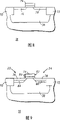
图1为现有技术中已知的电路的电路图;
图2为根据本发明的一个实施例制成的图1的电路的俯视图;
图3-6为图2的一部分电路处理过程中的顺序剖面图;以及
图7-9为图2的另一部分电路处理过程中的顺序剖面图。
具体实施方式
通过注入到栅极介质材料内以获得衬底中形成的源/漏和另一晶体管的栅极之间的连接,实现漏极到栅极的标准连接。通过注入到该区域中的栅极材料内由此在位置中的栅极介质变得导电,实现栅极材料和衬底之间的连接,从而栅极材料和源/漏之间的连接。通过参考附图和下面的介绍可以更好地理解。
图1所示的是在现有技术中已知的电路10,在集成电路中很常见,但是与现有技术的电路不同地制成并且与现有技术中的电路不同地配置而成。电路10包括晶体管12和晶体管14。晶体管12具有栅极16、源/漏18以及源/漏20。如这里所使用的,源/漏为与栅极相邻的掺杂区,可以是源或漏,取决于它在给定电路中的如何使用。晶体管14具有源/漏22和源/漏24。所显示的源/漏18、22以及24没有连接,但是在完整的电路中它们将具有与任一其它电路与电源端子的连接。类似地,栅极16将连接到其它电路或参考或信号。源/漏20连接到晶体管14的栅极26。源/漏到栅极的连接在晶体管中很常见。
图2所示的是根据本发明的一个实施例布局中的电路10。电路10包括有源区28和有源区30。有源区28用于形成晶体管12,有源区30用于形成晶体管14。栅极26覆盖在有源区30上并在接触32处连接到晶体管14的源/漏20。有源区28具有覆盖它的栅极16,并且含有源/漏18和20。有源区30含有源/漏22和24。通过注入至少部分该区域由此该区域中的栅极介质材料变得导电获得接触32。由此,在有源区18上延伸的栅极26通过接触32与漏20接触。
图3所示的是处理过程中较早阶段的晶体管12和14。处理过程中的该阶段为常规结构。电路10包括衬底38,为P型,具有P阱34和N阱36。所显示的衬底38具有P阱34和N阱36上并覆盖栅极介质材料46和48的导电材料50。P阱34位于隔离区40和42之间。在图3中N阱36位于隔离区42和44之间。图3中覆盖隔离区40和42之间的是栅极介质材料46,隔离区42和44之间是栅极介质材料48。覆盖栅极介质材料46和48的是多晶硅层50。衬底38也可以是绝缘体上硅(SOI),此时在绝缘体上存在半导体层。阱34和36将位于半导体层中,并且隔离区40,42和44将延伸到绝缘体。
图4所示的是已淀积光致抗蚀剂52并图案化之后由此在有源区28中用于接触32的位置中存在开口的电路10。图中示出了注入的中心深度在接触区32中的介质材料46处。结果为P阱34中的掺杂区33、注入的栅极介质35以及注入的多晶硅区37。有效的掺杂材料为硼,用于使接触32处的介质材料46成为高导电性。栅极介质材料可以是其它材料,并且代替多晶硅,栅电极也可以由其它材料形成。此时,需要提供除硼之外的不同掺杂剂,以形成需要的导电性以及栅极介质材料和覆盖的栅极材料之间的短路。一种所述掺杂剂为铝,另一种为磷。使用磷很有利,当注入到P阱内时,产生N型导电类型。除氧化硅之外的栅极介质材料可以是氧化铪。也可以选择其它材料。由此,对多晶硅形成了短路,同时在形成短路之前多晶硅没有被蚀刻。在常规的埋置接触中,需要将要接触的阱或区域开口,之后进行多晶硅淀积。就顺序而言,随后的蚀刻不仅不方便而且在衬底被暴露之后与要蚀刻的多晶硅相邻的衬底区域被蚀刻。
图5所示的是图案化蚀刻在栅介质材料46形成的栅极介质54上留下栅极16之后的多晶硅50和栅极材料46。同样,使用栅极16作为掩模形成源/漏扩展区56以及源/漏扩展区58。通过注入砷和磷的组合形成N型的源/漏扩展区56和58。可以根据需要改变注入的特定物质(species)和物质的组合。同样产生延伸到接触区32的栅极26。由此,栅极26与被注入的栅极介质材料区重叠。被注入的那部分栅极介质为最终形成栅极26和漏20之间接触的那部分,由此蚀刻多晶硅50之后,必须保留该注入的栅极材料的一部分。也可能需要在扩展区56和58之前进行组合的硼和铟的晕轮注入(halo implant)。没有显示该晕轮注入是由于晕轮注入在本领域中很公知,没有必要使附图变得复杂。
图6所示的是形成了侧壁以及组合的硼和铟注入以形成重掺杂的源/漏区60和62之后的电路10。栅极16具有侧壁间隔层64和66。栅极26具有侧壁间隔层68和70。该图示出了完整的N沟道型的晶体管12和完整的P沟道型的晶体管14。栅极26连接到接触32处的漏20。漏20由重掺杂的区域62和扩展区58组成。如果用磷注入接触区32,那么接触区会延伸穿过源/漏扩展区58,如图6所示。然而,如果接触区32掺有硼,形成P型区,那么接触区32不会横向延伸穿过源/漏扩展区58。栅极介质材料的掺杂区导电,由此将接触下面的掺杂区。如果该掺杂栅极介质仅接触源/漏,那么将仅短路栅极26到漏20,而不是到阱34。如果栅极介质的掺杂部分横向地延伸穿过漏20,那么它应该接触与阱34导电类型相反的掺杂区,由此图6所示的栅极介质的注入应形成N型区。
图7所示的是与图3所示相同处理阶段的晶体管14。在该剖面中,图7示出了N阱36和隔离区70和72以及栅极介质材料48。
图8所示的是已蚀刻多晶硅50形成栅极74和源/漏扩展区76和78之后的晶体管14。以类似于图5所示的方式但是在不同的工艺步骤形成这些扩展区,是由于掺杂类型与用于晶体管12和晶体管14的掺杂类型不同。通过组合注入砷和硼形成这些源/漏扩展区。图8需要的这些步骤可以在图5的那些步骤之前或之后。
图9所示的是形成侧壁间隔层80和82提供了用于形成重掺杂的源/漏区84和86的掩模以便使用硼的组合通过注入形成源/漏区22和源/漏24之后的完整晶体管14。
由此可以看出,剖面图3-6和剖面图7-9所示的完整电路10示出了完整的晶体管12和完整的晶体管14,晶体管12的漏区连接到晶体管14的栅极,而没有必要在源/漏上施加任何导电材料实现该接触。这避免了与埋置接触有关的问题,并提供了一个晶体管的漏区与另一晶体管的栅极之间很紧凑的互连。这具有降低了对更高级互连的需求的效果,由此降低了工艺处理的复杂性和产生缺陷的机会。由此,通过减少面积,芯片面积整体降低,提供了降低成本同时没有使工艺显著复杂化的机会。
通过除晶体管之外的电路特征,例如电阻器,同样可以获得类似的益处。另一电路特征可以具有一个电极,例如多晶硅栅极26,在源/漏上延伸并借助如区域35的导电注入介质与其电接触,如图4、5和6所示。
以上针对具体实施例介绍了益处、其它优点以及解决问题的措施。然而,产生任何益处、其它优点或解决问题或者变得更显著的益处、其它优点、解决问题以及任何要素不构成任何或所有权利要求的关键、需要或必要的特征或要素。如这里所使用的,术语“包括”、“包含”、或任何其它变形意在覆盖非特有的包含,由此包括列出要素的工艺、方法、制品或设备不仅包括这些要素,而是可以包括没有明确列出或这些工艺、方法、制品或设备固有的那些要素。
Claims (7)
1.一种形成电接触的方法,包括下列步骤:
提供半导体衬底;
在半导体衬底上形成栅极介质层;
在栅极介质层上形成导电层;
在形成所述导电层的步骤之后,将第一物质注入到栅极介质层的第一部分内,以改变该第一部分栅极介质,从而形成导电的、所述栅极介质的变换了的第一部分;
图案化所述导电层以形成图案化的导电层,该图案化的导电层包括第一栅、第二栅和从第一栅延伸到至少一部分在所述栅极介质的变换了的第一部分上的区域的延伸部分;
图案化所述栅极介质层,留下该栅极介质层的至少变换了的第一部分,以及
在与所述第二栅相邻的衬底上形成源/漏,其中所述源/漏具有在栅极介质的所述变换了的第一部分的至少一部分之下的一部分;
从而在所述第一栅和所述源/漏之间至少贯穿一部分所述变换了的那部分栅极介质地形成电接触。
2.根据权利要求1的方法,其中,将第一物质注入到栅极介质层的第一部分内的步骤包括:
在所述导电层上形成图案化的光致抗蚀剂层;以及
穿过导电层注入到所述栅极介质的第一部分。
3.根据权利要求1的方法,其中,所述第一物质包括硼。
4.根据权利要求3的方法,其中,所述图案化所述栅极介质层的步骤使用图案化了的光致抗蚀剂层作为掩模。
5.一种半导体器件,包括:
第一晶体管,该第一晶体管包括:
形成在衬底上的第一栅极介质;
形成在第一栅极介质上的第一栅电极;
形成在衬底内与第一栅极介质相邻的第一导电区;和
形成在衬底内与第一栅极介质相邻的第二导电区;以及第二晶体管,该第二晶体管包括:
形成在衬底上的第二栅极介质;
形成在第二栅极介质上的第二栅电极;
形成在衬底内与第二栅极介质相邻的第三导电区;和
形成在衬底内与第二栅极介质相邻的第四导电区;以及在所述第二栅极介质上并延伸到所述第三导电区域的一个区域的、第一栅的导电延伸区;和
被注入成导电的、并位于所述第一栅的导电延伸区和第三导电区之间的所述第二栅极介质的一部分,由此使所述第一栅和所述第三导电区电接触。
6.根据权利要求5的半导体器件,其中,所述栅极介质的被注入成导电的一部分是用硼注入的。
7.根据权利要求5的半导体器件,其中,所述第一晶体管在n型阱中,而所述第二晶体管在p型阱中。
Applications Claiming Priority (2)
| Application Number | Priority Date | Filing Date | Title |
|---|---|---|---|
| US09/986,232 | 2001-10-22 | ||
| US09/986,232 US6555915B1 (en) | 2001-10-22 | 2001-10-22 | Integrated circuit having interconnect to a substrate and method therefor |
Publications (2)
| Publication Number | Publication Date |
|---|---|
| CN1592951A CN1592951A (zh) | 2005-03-09 |
| CN1326210C true CN1326210C (zh) | 2007-07-11 |
Family
ID=25532216
Family Applications (1)
| Application Number | Title | Priority Date | Filing Date |
|---|---|---|---|
| CNB028231287A Expired - Fee Related CN1326210C (zh) | 2001-10-22 | 2002-09-27 | 具有到衬底的互连的集成电路及其方法 |
Country Status (7)
| Country | Link |
|---|---|
| US (1) | US6555915B1 (zh) |
| EP (1) | EP1479101A2 (zh) |
| JP (1) | JP2006500759A (zh) |
| KR (1) | KR20040048985A (zh) |
| CN (1) | CN1326210C (zh) |
| AU (1) | AU2002327714A1 (zh) |
| WO (1) | WO2003036702A2 (zh) |
Families Citing this family (15)
| Publication number | Priority date | Publication date | Assignee | Title |
|---|---|---|---|---|
| JP2003031801A (ja) * | 2001-07-16 | 2003-01-31 | Oki Electric Ind Co Ltd | 電界効果型トランジスタの製造方法 |
| US20040121524A1 (en) * | 2002-12-20 | 2004-06-24 | Micron Technology, Inc. | Apparatus and method for controlling diffusion |
| US7297617B2 (en) * | 2003-04-22 | 2007-11-20 | Micron Technology, Inc. | Method for controlling diffusion in semiconductor regions |
| US7654221B2 (en) * | 2003-10-06 | 2010-02-02 | Applied Materials, Inc. | Apparatus for electroless deposition of metals onto semiconductor substrates |
| US7297605B2 (en) * | 2004-05-10 | 2007-11-20 | Texas Instruments Incorporated | Source/drain extension implant process for use with short time anneals |
| DE102004038369B4 (de) * | 2004-08-06 | 2018-04-05 | Austriamicrosystems Ag | Hochvolt-NMOS-Transistor und Herstellungsverfahren |
| US7150516B2 (en) * | 2004-09-28 | 2006-12-19 | Hewlett-Packard Development Company, L.P. | Integrated circuit and method for manufacturing |
| KR100657142B1 (ko) * | 2005-06-03 | 2006-12-13 | 매그나칩 반도체 유한회사 | 이미지센서의 픽셀 쉬링크를 위한 콘택 구조 및 그 제조방법 |
| WO2016010053A1 (ja) * | 2014-07-14 | 2016-01-21 | 矢崎総業株式会社 | 電気素子 |
| JP6268070B2 (ja) * | 2014-09-16 | 2018-01-24 | 矢崎総業株式会社 | メッキ材及び端子金具 |
| JP6272744B2 (ja) * | 2014-10-24 | 2018-01-31 | 矢崎総業株式会社 | 板状導電体及び板状導電体の表面処理方法 |
| JP6374718B2 (ja) * | 2014-07-14 | 2018-08-15 | 矢崎総業株式会社 | 電気素子 |
| JP6268055B2 (ja) * | 2014-07-15 | 2018-01-24 | 矢崎総業株式会社 | 端子及びコネクタ |
| US10038081B1 (en) | 2017-09-06 | 2018-07-31 | Nxp Usa, Inc. | Substrate contacts for a transistor |
| US10679987B2 (en) * | 2017-10-31 | 2020-06-09 | Taiwan Semiconductor Manufacturing Co., Ltd. | Bootstrap metal-oxide-semiconductor (MOS) device integrated with a high voltage MOS (HVMOS) device and a high voltage junction termination (HVJT) device |
Citations (4)
| Publication number | Priority date | Publication date | Assignee | Title |
|---|---|---|---|---|
| EP0342778A1 (en) * | 1988-03-24 | 1989-11-23 | Nortel Networks Corporation | Ion implanted semiconductor device |
| US5087589A (en) * | 1987-06-12 | 1992-02-11 | Massachusetts Institute Of Technology | Selectively programmable interconnections in multilayer integrated circuits |
| JP2000031296A (ja) * | 1998-06-30 | 2000-01-28 | Motorola Inc | Cmos半導体素子およびその形成方法 |
| US6262486B1 (en) * | 1997-04-01 | 2001-07-17 | Micron Technology, Inc. | Conductive implant structure in a dielectric |
Family Cites Families (7)
| Publication number | Priority date | Publication date | Assignee | Title |
|---|---|---|---|---|
| JPH03101255A (ja) * | 1989-09-14 | 1991-04-26 | Sony Corp | 半導体装置 |
| JPH04162519A (ja) * | 1990-10-24 | 1992-06-08 | Sony Corp | Mos型半導体装置の製造方法 |
| US5783469A (en) * | 1996-12-10 | 1998-07-21 | Advanced Micro Devices, Inc. | Method for making nitrogenated gate structure for improved transistor performance |
| US6074904A (en) * | 1998-04-21 | 2000-06-13 | Advanced Micro Devices, Inc. | Method and structure for isolating semiconductor devices after transistor formation |
| US6077748A (en) * | 1998-10-19 | 2000-06-20 | Advanced Micro Devices, Inc. | Advanced trench isolation fabrication scheme for precision polysilicon gate control |
| KR100281908B1 (ko) * | 1998-11-20 | 2001-02-15 | 김덕중 | 반도체소자 및 그 제조방법 |
| JP3723410B2 (ja) * | 2000-04-13 | 2005-12-07 | 三洋電機株式会社 | 半導体装置とその製造方法 |
-
2001
- 2001-10-22 US US09/986,232 patent/US6555915B1/en not_active Expired - Fee Related
-
2002
- 2002-09-27 JP JP2003539091A patent/JP2006500759A/ja active Pending
- 2002-09-27 WO PCT/US2002/030337 patent/WO2003036702A2/en active Application Filing
- 2002-09-27 CN CNB028231287A patent/CN1326210C/zh not_active Expired - Fee Related
- 2002-09-27 AU AU2002327714A patent/AU2002327714A1/en not_active Abandoned
- 2002-09-27 EP EP02763717A patent/EP1479101A2/en not_active Withdrawn
- 2002-09-27 KR KR10-2004-7006013A patent/KR20040048985A/ko active Search and Examination
Patent Citations (4)
| Publication number | Priority date | Publication date | Assignee | Title |
|---|---|---|---|---|
| US5087589A (en) * | 1987-06-12 | 1992-02-11 | Massachusetts Institute Of Technology | Selectively programmable interconnections in multilayer integrated circuits |
| EP0342778A1 (en) * | 1988-03-24 | 1989-11-23 | Nortel Networks Corporation | Ion implanted semiconductor device |
| US6262486B1 (en) * | 1997-04-01 | 2001-07-17 | Micron Technology, Inc. | Conductive implant structure in a dielectric |
| JP2000031296A (ja) * | 1998-06-30 | 2000-01-28 | Motorola Inc | Cmos半導体素子およびその形成方法 |
Also Published As
| Publication number | Publication date |
|---|---|
| AU2002327714A1 (en) | 2003-05-06 |
| WO2003036702A3 (en) | 2003-11-06 |
| US20030075806A1 (en) | 2003-04-24 |
| JP2006500759A (ja) | 2006-01-05 |
| CN1592951A (zh) | 2005-03-09 |
| KR20040048985A (ko) | 2004-06-10 |
| WO2003036702A2 (en) | 2003-05-01 |
| EP1479101A2 (en) | 2004-11-24 |
| US6555915B1 (en) | 2003-04-29 |
Similar Documents
| Publication | Publication Date | Title |
|---|---|---|
| CN1326210C (zh) | 具有到衬底的互连的集成电路及其方法 | |
| US4764480A (en) | Process for making high performance CMOS and bipolar integrated devices on one substrate with reduced cell size | |
| EP0883184B1 (en) | Use of a camouflaged circuit | |
| CN101937874B (zh) | 产生不对称场效应晶体管的方法 | |
| KR100339024B1 (ko) | 플래쉬메모리장치의센스앰프회로 | |
| JPH10294430A (ja) | Soi集積回路のesd保護用の双安定擬似scrスイッチ | |
| KR20010033347A (ko) | 벌크 씨모스 구조와 양립 가능한 에스오아이 구조 | |
| JP2006500759A5 (zh) | ||
| KR100339025B1 (ko) | 플래쉬메모리셀의제조방법 | |
| US5985733A (en) | Semiconductor device having a T-shaped field oxide layer and a method for fabricating the same | |
| KR100419674B1 (ko) | 반도체장치및그제조방법 | |
| CN100388427C (zh) | 用于制造具有多栅氧化膜的半导体器件的方法 | |
| US6621116B2 (en) | Enhanced EPROM structures with accentuated hot electron generation regions | |
| US6921690B2 (en) | Method of fabricating enhanced EPROM structures with accentuated hot electron generation regions | |
| US5707721A (en) | Methods of forming field effect transistors having oxidation-controlled gate lengths | |
| KR0135691B1 (ko) | 트랜지스터 및 그 제조방법 | |
| KR20040081048A (ko) | 반도체 장치 및 그 제조 방법 | |
| KR100451042B1 (ko) | 반도체소자의콘택형성방법 | |
| KR100347145B1 (ko) | 플래시 셀 배열에서 세그먼트 트랜지스터와 셀 영역의연결방법 | |
| JP2985845B2 (ja) | 半導体装置およびその製造方法 | |
| KR100349376B1 (ko) | 트렌치 측벽을 채널층으로 사용하는 트렌치 트랜지스터의제조 방법 | |
| JPH08321593A (ja) | リード・オンリ・メモリ装置とその製造方法 | |
| TW276355B (en) | Integrated circuit with planar conductive layer structure | |
| KR100444772B1 (ko) | 상보형 모스 트랜지스터의 제조방법 | |
| KR100309126B1 (ko) | 반도체 소자 형성 방법 |
Legal Events
| Date | Code | Title | Description |
|---|---|---|---|
| C06 | Publication | ||
| PB01 | Publication | ||
| C10 | Entry into substantive examination | ||
| SE01 | Entry into force of request for substantive examination | ||
| C14 | Grant of patent or utility model | ||
| GR01 | Patent grant | ||
| C17 | Cessation of patent right | ||
| CF01 | Termination of patent right due to non-payment of annual fee |
Granted publication date: 20070711 Termination date: 20110927 |