CN1139984A - 并列的光学互连接 - Google Patents
并列的光学互连接 Download PDFInfo
- Publication number
- CN1139984A CN1139984A CN94192730.XA CN94192730A CN1139984A CN 1139984 A CN1139984 A CN 1139984A CN 94192730 A CN94192730 A CN 94192730A CN 1139984 A CN1139984 A CN 1139984A
- Authority
- CN
- China
- Prior art keywords
- mentioned
- optical fiber
- fiber
- array
- optical
- Prior art date
- Legal status (The legal status is an assumption and is not a legal conclusion. Google has not performed a legal analysis and makes no representation as to the accuracy of the status listed.)
- Pending
Links
Images


Classifications
-
- G—PHYSICS
- G02—OPTICS
- G02B—OPTICAL ELEMENTS, SYSTEMS OR APPARATUS
- G02B6/00—Light guides; Structural details of arrangements comprising light guides and other optical elements, e.g. couplings
- G02B6/24—Coupling light guides
- G02B6/245—Removing protective coverings of light guides before coupling
-
- G—PHYSICS
- G02—OPTICS
- G02B—OPTICAL ELEMENTS, SYSTEMS OR APPARATUS
- G02B6/00—Light guides; Structural details of arrangements comprising light guides and other optical elements, e.g. couplings
- G02B6/24—Coupling light guides
- G02B6/42—Coupling light guides with opto-electronic elements
-
- G—PHYSICS
- G02—OPTICS
- G02B—OPTICAL ELEMENTS, SYSTEMS OR APPARATUS
- G02B6/00—Light guides; Structural details of arrangements comprising light guides and other optical elements, e.g. couplings
- G02B6/24—Coupling light guides
- G02B6/42—Coupling light guides with opto-electronic elements
- G02B6/4201—Packages, e.g. shape, construction, internal or external details
- G02B6/4202—Packages, e.g. shape, construction, internal or external details for coupling an active element with fibres without intermediate optical elements, e.g. fibres with plane ends, fibres with shaped ends, bundles
-
- G—PHYSICS
- G02—OPTICS
- G02B—OPTICAL ELEMENTS, SYSTEMS OR APPARATUS
- G02B6/00—Light guides; Structural details of arrangements comprising light guides and other optical elements, e.g. couplings
- G02B6/24—Coupling light guides
- G02B6/42—Coupling light guides with opto-electronic elements
- G02B6/4201—Packages, e.g. shape, construction, internal or external details
- G02B6/4219—Mechanical fixtures for holding or positioning the elements relative to each other in the couplings; Alignment methods for the elements, e.g. measuring or observing methods especially used therefor
- G02B6/4228—Passive alignment, i.e. without a detection of the degree of coupling or the position of the elements
- G02B6/423—Passive alignment, i.e. without a detection of the degree of coupling or the position of the elements using guiding surfaces for the alignment
- G02B6/4231—Passive alignment, i.e. without a detection of the degree of coupling or the position of the elements using guiding surfaces for the alignment with intermediate elements, e.g. rods and balls, between the elements
-
- G—PHYSICS
- G02—OPTICS
- G02B—OPTICAL ELEMENTS, SYSTEMS OR APPARATUS
- G02B6/00—Light guides; Structural details of arrangements comprising light guides and other optical elements, e.g. couplings
- G02B6/24—Coupling light guides
- G02B6/42—Coupling light guides with opto-electronic elements
- G02B6/4201—Packages, e.g. shape, construction, internal or external details
- G02B6/4219—Mechanical fixtures for holding or positioning the elements relative to each other in the couplings; Alignment methods for the elements, e.g. measuring or observing methods especially used therefor
- G02B6/4228—Passive alignment, i.e. without a detection of the degree of coupling or the position of the elements
- G02B6/4232—Passive alignment, i.e. without a detection of the degree of coupling or the position of the elements using the surface tension of fluid solder to align the elements, e.g. solder bump techniques
-
- G—PHYSICS
- G02—OPTICS
- G02B—OPTICAL ELEMENTS, SYSTEMS OR APPARATUS
- G02B6/00—Light guides; Structural details of arrangements comprising light guides and other optical elements, e.g. couplings
- G02B6/24—Coupling light guides
- G02B6/42—Coupling light guides with opto-electronic elements
- G02B6/4201—Packages, e.g. shape, construction, internal or external details
- G02B6/4249—Packages, e.g. shape, construction, internal or external details comprising arrays of active devices and fibres
-
- G—PHYSICS
- G02—OPTICS
- G02B—OPTICAL ELEMENTS, SYSTEMS OR APPARATUS
- G02B6/00—Light guides; Structural details of arrangements comprising light guides and other optical elements, e.g. couplings
- G02B6/24—Coupling light guides
- G02B6/42—Coupling light guides with opto-electronic elements
- G02B6/4201—Packages, e.g. shape, construction, internal or external details
- G02B6/4204—Packages, e.g. shape, construction, internal or external details the coupling comprising intermediate optical elements, e.g. lenses, holograms
- G02B6/421—Packages, e.g. shape, construction, internal or external details the coupling comprising intermediate optical elements, e.g. lenses, holograms the intermediate optical component consisting of a short length of fibre, e.g. fibre stub
-
- G—PHYSICS
- G02—OPTICS
- G02B—OPTICAL ELEMENTS, SYSTEMS OR APPARATUS
- G02B6/00—Light guides; Structural details of arrangements comprising light guides and other optical elements, e.g. couplings
- G02B6/24—Coupling light guides
- G02B6/42—Coupling light guides with opto-electronic elements
- G02B6/4201—Packages, e.g. shape, construction, internal or external details
- G02B6/4219—Mechanical fixtures for holding or positioning the elements relative to each other in the couplings; Alignment methods for the elements, e.g. measuring or observing methods especially used therefor
- G02B6/422—Active alignment, i.e. moving the elements in response to the detected degree of coupling or position of the elements
- G02B6/4221—Active alignment, i.e. moving the elements in response to the detected degree of coupling or position of the elements involving a visual detection of the position of the elements, e.g. by using a microscope or a camera
- G02B6/4224—Active alignment, i.e. moving the elements in response to the detected degree of coupling or position of the elements involving a visual detection of the position of the elements, e.g. by using a microscope or a camera using visual alignment markings, e.g. index methods
-
- G—PHYSICS
- G02—OPTICS
- G02B—OPTICAL ELEMENTS, SYSTEMS OR APPARATUS
- G02B6/00—Light guides; Structural details of arrangements comprising light guides and other optical elements, e.g. couplings
- G02B6/24—Coupling light guides
- G02B6/42—Coupling light guides with opto-electronic elements
- G02B6/4201—Packages, e.g. shape, construction, internal or external details
- G02B6/4246—Bidirectionally operating package structures
-
- G—PHYSICS
- G02—OPTICS
- G02B—OPTICAL ELEMENTS, SYSTEMS OR APPARATUS
- G02B6/00—Light guides; Structural details of arrangements comprising light guides and other optical elements, e.g. couplings
- G02B6/24—Coupling light guides
- G02B6/42—Coupling light guides with opto-electronic elements
- G02B6/43—Arrangements comprising a plurality of opto-electronic elements and associated optical interconnections
Landscapes
- Physics & Mathematics (AREA)
- General Physics & Mathematics (AREA)
- Optics & Photonics (AREA)
- Optical Couplings Of Light Guides (AREA)
- Optical Integrated Circuits (AREA)
Abstract
本发明公开了一种将许多光纤(135)耦联到光电器件阵列上的光学互连接。此光学互连接包括一多光纤连接器(150)及一光电子插件板(100)。该多光纤连接器(150)能以机械方式固定到该插件板(100),或从中取出。
Description
本发明的技术领域
本发明涉及光学互连接,更确切地说,涉及将多根光纤耦联在整体形成的光电子器件阵列上的光学互连接。
本发明的背景技术
光纤技术已经广泛应用在当今的通信网中。它还是未来产生出预计要变革人们交换或取得信息方式的通信技术的基础。
光纤技术的一个重要方面,在于将光纤互连在象半导体激光器、光探测器之类光电子器件上,其中的光电子器件不是接收来自光纤的光学辐射,就是由光电子器件将光学辐射发射到光纤中。光纤和光电子器件间优良的光学互连接,要求高的耦合效率(即来自该耦合的光损耗低)、构成耦合容易,而且构成这种互连接的成本低。
将光纤耦联在光电子器件上的传统方法是通过有源对准。例如,为了通过有源对准将半导体激光器耦联到光纤上,首先要接通该激光器以发出光辐射。然后将光纤的耦合端放在靠近该激光器的光发射表面,以接收光辐射,并且在光纤的另一端放置光探测器,以探测被耦合到光纤中的光辐射的大小。然后围绕激光器的发光表面手动变换光纤耦合端的位置,直到处在光纤另一端的光探测器检测到最大光辐射为止。然后将光学环氧树脂胶加在激光器和光纤的耦合端,以便永久性保持这种优化的耦合。
按照类似方式,通过将激光发进光纤的一端,并且手动调节打算耦联到探测器上的光纤另一端的位置,直到该探测器对于光辐射的电响应达到最大为止,可以将光探测器耦联到光纤上面。然后将光学环氧树脂胶加上,以将光纤附着在探测器上。
然而由于半导体激光器发光表面和光纤截面的尺寸都非常小,例如对于单模光纤在10μm的数量级,所以将半导体激光器耦联在光纤上,通常是一项费时的工作,并且需要专门知识和经验。就光纤耦联到光探测器上而论,即使人们可以增大探测器的尺寸以使这种耦联变得较为容易,然而增加探测器尺寸将不希望地增加探测器的寄生现象,从而累及探测器的工作速度和频率响应。
上述光学互连接的问题之一,是在热应变之下光纤和光电器件间的对准可能遭遇不对准之苦。这种热应变的产生,是当此互连接的温度升高时,即由于光电器件和该器件的驱动电路产生的热,或通过其它各种因素,如附近的电子元件。
而且,由于光电器件阵列是整体加工在半导体晶片上的,通常包括大量密集的器件,故应用上述有源对准方法将许多光纤耦联在此光电器件阵列上也是不实际的。然而经过许多光纤将例如光电发射器件阵列耦联在如光电探测器阵列之上,在需要并联耦合许多信号的如局域网(LAN)中应用,可能是非常有用的。
因此,本发明的目的,在于提供能够将许多光纤机械地耦联到整体形成的光电器件阵列上的光学互连接。
发明概述
本发明为一种用于将多根光纤耦联在光电器件阵列上的光学互连接。
在本发明的第一实施例中,此光学互连接包括一个能同光电子插件板耦联的多光纤连接器。
该多光纤连接器包括一个至少带有一个平面的夹持器,许多光纤被固定在此夹持器上,每一光纤都带有邻接第一表面的耦合端,为的是使此耦合端暴露,以便接收或发射光辐射;并由这些光纤的第一端形成一光纤阵列,而且导向机构相对此光纤阵列按预定位置配置在夹持器中。
光电子插件板包括一光电器件阵列,基本上按照光纤阵列的同样图案被整体加工在半导体晶片上。该插件板进一步包括有对准机构,基本上按照导向机构相对于光纤阵列定位的方式,以同样的预定位置相对于光电器件阵列加工在半导体晶片上。
通过让导向机构对正并啮合在对准机构中,便可使光纤连接器耦联在光电子插件板上,从而使光电器件阵列与光纤阵列对准,并使每一光电器件耦联在光纤上。最好让导向机构为导向杆,且对准机构为晶片上加工的对准孔。
此光电器件可以是能将光辐射发射到光纤阵列中的光电发射器,或者是能够接收由光纤阵列中发出光辐射的光电探测器。
在第二实施例中,此光学互连接包括多光纤连接器和光电子插件板。其中光纤连接器与第一实施例中相同。
光电子插件板包括一带有第一表面及第一对准机构的基板、装在该基板第一表面上的半导体晶片,以及整体加工在该晶片上的光电器件阵列。这些光电器件基本上按照光纤阵列的同样图案安排在晶片上。该光电子插件板进一步还包括第二个对准机构,用于使光电器件阵列与第一对准机构对准。第一对准机构则按照导向机构相对光纤阵列定位的方式,相对于光电器件阵列被定位在基本相同的预定位置。
通过让导向机构对正并啮合到对准机构中,便可使光纤连接器耦联在光电子插件板上,从而使光电器件阵列与光纤阵列对准,而且每一光电器件均与光纤耦合。最好让导向机构为导向杆,且对准机构为基板上加工出来的对准孔。而且光电器件可以是光电发射器或光电探测器。
本发明能够使由于互连接中使用的不同材料间热膨胀失配,引起热应变造成的不对准减少。这是通过让光纤组件锚定导杆位置来达到的。
在本发明的第三实施例中,光学互连接包括有光纤以及耦联在该光纤耦合端的竖直腔面发射激光器(VCSEL)。
光纤包括芯和环绕该芯的包层。处在光纤耦合端的光纤芯是凹进去的,以便形成显示边缘的结构,其中的边缘基本上由包层组成。
竖直腔面发射激光器,包括半导体基片、在上述基片上面形成的第一反射镜、与第一反射镜平行且位于其上的第二反射镜,并由其与第一反射镜一起构成与基片垂直的光学腔,并且包括由上述反射镜间配置的第一和第二个垫片环绕的活性区。
第一和第二个反射镜为布喇格分布的反射镜,并且包括一层在另一层顶部而形成的许多层。上述第二反射镜的许多最外层组成一高台,其直径小于上述光纤边缘的内径。此高台与上述显出边缘的结构啮合,以将所述高台的主体部分安置在该边缘内部。其结果是该激光器自动对准,而且该激光器发出的光辐射被充分耦合到上述光纤中。
这种光学互连接,由于激光器被嵌入光纤之中,故能够减少由热应变引起的不对准。
附图的简要描述
本发明的这些以及其它一些目的、性能和优点,从以下结合附图所作的详细描述中将会更加清楚,其中:
图1a表示本发明光学互连接第一实施例的三维视图;
图1b表示图1a中表面130的视图;
图2表示本发明第二实施例;
图3表示图2的组装的互连接;
图4a和4b表示本发明互连接的应用;
图5a至5c表示本发明光学互连接的第三实施例,以及
图6a和6b表示图5a至5c中光学互连接的阵列。
详细描述
根据本发明第一实施例的光学互连接,包括有多光纤连接器和光电子插件板。该连接器包括夹持器、固定在夹持器上的许多光纤和导向机构。光电子插件板包括整体加工在半导体晶片上的光电器件阵列,以及限定在该晶片上的对准机构。通过机械方式使光纤连接器的导向机构与插件板的对准机构啮合,便可将光纤耦联在光电器件阵列上。
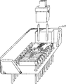
图1a表示此光学互连接的优选实施例。它包括光纤连接器150和光电子插件板100。
此光纤连接器150包括带有平面130的夹持器125,许多光纤135被嵌在该夹持器中,而且两个导向杆140可滑动地安装在两上圆柱孔道141中。
这些光纤具有耦合端131,沿竖直方向与表面130邻接。该光纤的耦合端被暴露出来,以便接收或发射光辐射。如图1b中表面130端视图表示的那样,由耦合端131形成了一维光纤阵列132。在此光纤阵列中,任意两根光纤间的距离,等于其它任意两相邻光纤的距离。最好使任意两相邻光纤中心间的距离约为0.25mm。
孔道141和杆140相对此光纤阵列对称定位,其相对光纤阵列的位置被预先确定。
光电子插件板100包括半导体晶片105、整体加工在此半导体晶片上的一维光电器件阵列110,以及用于连接这些光电器件的许多导线115。该晶片包含两个对准孔120,大约具有与孔道141相同的直径以接纳导杆。比较有利的作法是使光电器件阵列110和插件板的对准孔120基本上具有如光纤阵列132和光纤连接器上孔道141所形成的同样图案,即任意两相邻光电器件中心间的距离与任意两相邻光纤中心间的距离相等。因此,简单地通过让光纤连接器上孔道中的导杆140与光电插件板上的对准孔120啮合,便可使光纤阵列沿轴向与光电器件阵列对准。每一光纤也和相应的光电器件对准。
与图1a表示的光学连接器类似的光学连接器,已被公开在Hayashi等人的欧洲专利申请公开No.0,226,274中,在此被引用作为参考。具有两相邻光纤中心容限差为10μm数量级的同一类型的光学连接器从市场上可以买到。
半导体晶片上的光电器件阵列和对准孔是通过发展良好的半导体加工工艺确定的,例如光刻以及化学或活性离子蚀刻。因而器件面貌或对准孔的公差可控制在10μm数量级之内。将此公差与可买到的光纤连接器的紧公差结合,这种互连接能够提供很好的耦合效率,而且能够容易地连接或者断开。
该光纤可以是单模或者多模光纤,例如塑料光纤。然而该光纤最好是具有芯径从50到100μm范围的多模光纤。多模光纤通常具有比单模光纤更大的芯径,其结果是能比单模光纤提供更高的对准公差。
光电器件可以是各种类型的器件,如边缘发射激光器、超强发光二极管(SLED)、竖直腔面发光激光器(VCSEL)、其它面发光器件或光电探测器。它们还可以是组合一或更多种器件的集成器件,例如VCSEL和晶体管组合或者光探测器和晶体管组合。
当光电器件为VCSEL时,此光学互连接起到将光信号发送到光纤中的发射器的作用。一般说来,该连接中对准公差在2~20μm的范围内。例如每一VCSEL的直径约为20μm,而且每根光纤都是芯径约为62.5μm的多模光纤,其对准公差约为10μm。
该光学互连接进一步还可包括与VCSEL阵列互连的电子电路装置,以便驱动和调制VCSEL。这种电子电路装置可以整体加工在半导体晶片上面,或者作为混合集成电路与VCSEL阵列集成在一起。
假如光电器件是在半导体晶片上形成的光电探测器,则此光学互连接起到接收器的作用,以从光纤接收光信号。例如,如果每一光电探测器都是具有直径约为100μm的肖特基势垒光电探测器,而且每根光纤都是具有芯径约62.5μm的多模光纤,则光纤和探测器间的对准公差约为20μm。
在上述优选实施例中,所举的实例是一维阵列。然而也可类似地利用二维阵列,以形成二维的光学互连接。
在本发明的第二实施例中,此光学互连接也包括一个光学连接器和一个光电子插件板。该连接器包括一个夹持器、固定在夹持器中的许多光纤和导向机构。光电子插件板包括一个基板、配置在该基板之上的半导体晶片,以及整体加工在此半导体晶片上的光电器件阵列。此光电子插件板进一步还包括加工在基板上的第一对准机构和配置在晶片和基板之间的第二对准机构,以使光电器件阵列相对第一对准机构正确地定位。通过以机械方式让连接器的导向机构与插件板的第一对准机构对准和啮合,便可将光纤耦联在光电器件阵列之上。
图2a表示此光学互连接的优选实施例,它包括一个光学连接器150和一个光电子插件板101。为方便起见,图2a及2b中相同的元件用图1中同样的编号表示。本实施例中的光纤连接器150是和第一实施例中的光学连接器相同的,因而在此不作评述。
光电子插件板101包括一块绝缘的基板90、配置在该基板上的半导体晶片105、整体加工在该半导体晶片上的线性排列的光电器件阵列110、互连在该光电器件阵列上的电子电路装置117,以及限定在基板外围用于连接该电路装置的接触垫片108。此光电子插件板进一步还包括作为第一对准机构用的加工在基板上的两个对准孔119,以接纳导向杆。如图2b中表示的那样,此插件板进一步还包括第二个对准机构91,形成在半导体晶片的第二表面95和基板的第一表面96之间。第二对准机构沿横向让光电器件阵列与基板上形成的第一对准机构119对准。
构成这种光学互连接的原理如下:
首先在半导体晶片上加工出光电器件。这些器件被安排以构成具有如光纤阵列同样图案的阵列。利用发展得很好的半导体工艺,能够准确地限定该光电器件的位置,使得任意两相邻器件中心间的距离与任意两相邻光纤中心间的距离相等。
接下去采用如激光精密打孔工艺,在基板上确定出对准孔119。此对准孔基本上具有如光纤连接器中孔道141同样的直径,而且两对准孔中心间的距离基本上与两孔道间相同。因而导杆能同此对准孔对准。
然后通过利用倒装焊接工艺,沿横向将光电器件阵列与该对准孔对准。如图2b表示的那样,倒装焊接工艺主要包括的步骤是:在基板的第一表面96上形成第一组金属焊接点93,其图案相对对准孔119具有预定的位置,这是通过在基板上沉积一层焊料而后发生的。然后通过光刻和腐蚀使此焊料层构图,以在第一组金属图案的顶部形成第二组焊料图案94。第三组金属焊接点92乃是第一组焊接点的镜面反射像,是随后限定在半导体晶片的第二表面95上的。通过采用红外线对准技术,使第三组图案按照这样一种方式与光电器件阵列对准,从而使假如第三组图案沿竖直方向是和第一组图案对准的,则光电器件阵列将按一定方式沿横向与对准孔对准,从而使光电器件阵列也将沿竖直方向与光纤阵列对准。
第三组图案与第一组图案的对准,比较有利的作法是通过自动对准工艺。在自动对准工艺过程中,首先粗略地将第三组图案与第二组图案对准。然后加热以使焊料熔化。熔化了的焊料将约束在第三和第一金属图案间,而不沿横向流到该图案之外。由于该焊料表面张力的作用,第三组图案会自动地与第一组图案对准。当不加热时,焊料冷却,而且自动对准过程完成。此倒装焊接工艺在“倒装焊接使光学内部通信系统(ICS)优化”一文中已由Wale等人详细说明,参见IEEE电路和器件,1992,11,PP.25-31,在此引用作为参考。
因此,在此焊料流动自动对准过程完成时,光电器件阵列便按照光纤阵列对准导向杆的同样方式横向对准对准孔。所以,通过沿竖向将导向杆与对准孔对准和啮合,便可使光纤阵列对准并耦联在光电器件阵列上。
如图1a的光学互连接情况中那样,如果光电器件为VCSEL,而且电子电路装置117为驱动和调制VCSEL用的集成电路,则此互连接起到将光学信号射入光纤的光学发射器的作用。如果光电器件为光电探测器,则此互连接起到光学接收器的作用,以接收经过光纤发送的光学信号。光电探测器则将与此光学信号对应的电信号传送给电子电路装置,在其被转送给其它电路如计算机或处理器之前,对此信号进行处理。如果光电器件既包括VCSEL又包括光电探测器,则此光学互连接实际上既是发射器又是接收器。
应当指出,通过利用焊料流动自动对准工艺,可以使两或更多个单独的半导体晶片与一个光纤阵列对准。在这种情况下,一个晶片上的许多器件被耦联在光纤连接器一些光纤上,而其它晶片上的许多器件则耦联在其它一些光纤上。按照这种方式,发射器和接收器可被耦联在单个光学连接器上。
图3表示图2的光学互连接安装在20脚插件200中的情形。此光纤连接器能够很容易地固定到光电子插件板上或由其上取下。
图4表示本发明的光学互连接应用于插件板对插件板的互连接。在此应用中,插件板400经过连接器405和415被连接在插件板410上。图4b为放大表示连接器405或415。每一连接器405或415都包括一个如图1a或3表示的光学互连接。如果连接器405仅包含如发射器的光学互连接,而且连接器415仅包含如接收器的光学互连接,那么数据就只能从插件板400发送给插件板410。然而,如果连接器405和415两者都包括带有发射和接收器两者的光学互连接,那么数据可以按照全双工方式经过光纤带在插件板间传送。
在本发明的第三实施例中,光学互连接包括带有耦合端的光纤和耦联该光纤耦合端的竖直腔面发射激光器。
该光纤包括有芯和环绕在该芯周围的包层。处在光纤耦合端的光纤芯是凹进去的,以便形成显出边缘的结构,其中的边缘是由包层组成的。
竖直腔面发射激光器具有第二反射镜,是一个布喇格分布的反射器,包括一层在另一层顶部形成的许多层。比较有利地是由第二反射镜的许多最外层组成一高台,具有小于上述光纤边缘内径的直径。此高台与光纤耦合端啮合,以将高台的基本部分安置在此边缘内部。VCSEL发出的光辐射则基本上全被耦合到光纤中。
图5a至5c表示本发明的优选实施例。
具体说来,图5a表示光纤500和与其耦联之前的VCSEL的三维视图。光纤500包括有芯505和环绕该芯的包层510。在光纤的耦合端515,芯是凹进去的,以形成主要是由包层构成的边缘516。VCSEL则包括一由第二反射镜的许多最外层组成的高台555、图5b中描述的若干基底层和环绕高台的接头565。
图5b表示该光学互连接的剖面图。VCSEL包括有在基片520上面形成的第一反射镜525、第一垫片530、活性区535、第二垫片540、第二反射镜的一部分545,以及第二反射镜的高台部分555。它进一步还包括环绕高台的接头565和在基片上形成的接头575。此外,存在一保护大部分表面免受大气影响的钝化层560。此钝化层最好是SiO2层。该激光器进一步还包括一环绕活性区的环形注入电流限制层550。
第一和第二个反射镜两者都是布喇格分布的反射器,每一反射镜都包括一层形成在另一层顶部的许多层。此外,每层都是四分之一波长厚度,其中所述波长是在该层中的波长。高台555最好包括有介电层,而且层545为具有高掺杂浓度的半导体层,以与接头565形成的低电阻接触。
光纤的耦合端是通过光学环氧树脂胶570牢固地固定在VCSEL激光器上部的。
此互连接中的光纤可以是单模光纤、多模光纤或塑料光纤。
图5c表示这种互连接的三维视图。在此连接中,所有的光辐射基本上都被耦合到光纤中而不需要额外的对准机构。
这种互连接制备如下:首先如图5b所示制备好VCSEL激光器,随后制造在耦合端带有凹进芯的光纤。玻璃光纤的芯和包层通常均由二氧化硅制成。然而光纤芯通常要进行掺杂以提高其折射率,而后由缓冲的氢氟酸(BHF)或其它酸有选择地从包层中蚀刻它。接下去让蚀刻过的光纤与VCSEL激光器对准,并使其高台固定到边缘中。然后将光学环氧树脂胶加到光纤和激光器上。
这种互连接也可以做成一维或二维阵列,其中整体形成的VCSEL激光器阵列被耦联在光纤阵列上。
图6a及6b表示这种光学互连接的实例,其中光纤连接器650包括的光纤线性阵列,是和VCSEL激光器的线性阵列耦联的。具体说来,图6a表示VCSEL阵列和耦联之前的光纤阵列,而图6b则表示它们耦联之后的互连接。
在本实施例中,每一VCSEL激光器和每一光纤都具有如图5b中描述的相同结构,故不在此对其作详细描述。此外,可以通过利用光纤连接器中的一对孔道和导杆以及邻近VCSEL激光器阵列的对准孔,如图1~4实施例中描述的那样,让光纤连接器650对准并耦联在VCSEL激光器阵列上。
如本领域技术熟练人员将会明白的那样,在本发明的范围内能够作出许多改变,并不确定为下述权利要求限定的除外。
应当指出的是,在此整个说明过程中,光纤可以是单模光纤、多模光纤(例如塑料光纤)或其它类型的光纤;光电器件阵列可以是一维的或者二维的;光电器件可以是边缘发射激光器、高强发光二极管、光电探测器,或者其它任何类型的光电器件。它们全都在本发明的保护范围之内。
Claims (66)
1.一种光学互连接,包括有:
多光纤连接器,它包括:带有一第一平面的夹持器;固定在该夹持器中的许多光纤,其中每一光纤都具有一邻接上述第一平面的第一端,为的是使其暴露在外,以接收或发射光辐射,并由这些光纤第一端形成一具有第一图案的光纤阵列;以及相对该光纤阵列配置在上述夹持器中预定位置的导向机构,和
光电子插件板包括:一整体加工在半导体晶片上的光电器件阵列,所述光电器件阵列具有与上述光纤阵列的第一图案基本相同的图案;以及形成在上述晶片上的对准机构,所述对准机构如导向机构相对上述光纤阵列的位置那样,被配置在相对上述光电器件阵列为基本相同的预定位置,而且,
上述对准机构接纳上述导向机构,以使上述光电器件阵列与上述光纤阵列按机械方式对准,从而使每一光电器件对准一光纤,而由所述光电器件将光辐射发射到上述光纤阵列中,或由上述光纤阵列接收光辐射。
2.根据权利要求1的互连接,其中所述的导向机构包括两根安装在夹持器中的导杆,所述导杆穿过夹持器的上述第一平面伸出;而且所述对准机构包括两个对准孔,通过上述导杆与上述对准孔对准并啮合,以便使光纤阵列对准光电器件阵列。
3.根据权利要求2的互连接,其中所述光纤阵列是配置在两根导杆之间的。
4.根据权利要求1的互连接,其中所述导向机构包括两根安装在夹持器中的导杆,所述导杆沿垂直上述第一表面的方向穿过夹持器的上述第一平面伸出;而且所述对准机构包括两个对准孔,通过上述导杆与上述对准孔对准并啮合,以便使上述光纤阵列对准上述光电器件阵列。
5.根据权利要求4的互连接,其中所述光纤阵列是配置在上述两根导杆之间的。
6.根据权利要求1的互连接,其中的光纤形成一维阵列。
7.根据权利要求1的互连接,其中的光纤形成二维阵列。
8.根据权利要求6的互连接,其中的光电器件阵列包括一维阵列的竖直腔面发射激光器,每一激光器均沿轴向对准一光纤,且由光纤接收激光器发出的光辐射。
9.根据权利要求8的互连接,进一步包括互连在上述激光器阵列上的第一电子电路装置,以便驱动和调制上述激光器。
10.根据权利要求8的互连接,其中每一光纤均为塑料光纤。
11.根据权利要求8的互连接,其中每一光纤为单模光纤。
12.根据权利要求8的互连接,其中每一光纤为多模光纤。
13.根据权利要求12的互连接,其中每一多模光纤具有约为62.5μm的直径。
14.根据权利要求13的互连接,其中每一竖直腔面发射激光器具有约为20μm的直径。
15.根据权利要求6的互连接,其中的光电器件阵列包括一维的光电探测器阵列,每一光电探测器沿轴向与光纤端部对准,并由探测器接收激光器发射的光辐射。
16.根据权利要求15的互连接,其中的光电探测器为肖特基势垒光电探测器。
17.根据权利要求15的互连接,进一步包括用于接收来自光电探测器的电信号的第二电子电路装置。
18.根据权利要求16的互连接,其中每一光纤为多模光纤。
19.根据权利要求18的互连接,其中每一多模光纤具有约62.5μm的直径。
20.根据权利要求19的互连接,其中每一光电探测器具有约100μm的直径。
21.一种光电子互连接,包括有:
多光纤连接器,它包括:一个至少带有一个平面的夹持器;许多固定在夹持器上的光纤,每一光纤具有一邻接第一个表面的第一端,为的是使其暴露,以接收或发送光辐射,并由上述光纤的第一端形成一具有第一图案的光纤阵列;以及相对上述光纤阵列配置在上述夹持器中预定位置的导向机构,和
光电子插件板,它包括:具有第一表面和第一对准机构的基片;整体加工在半导体晶片第一表面上的光电器件阵列,所述光电器件阵列具有与上述光纤阵列的第一图案基本相同的图案,所述晶片配置在该基片上;第二对准机构,用于使上述光电器件阵列对准上述第一对准机构;上述第一对准机构如导向机构相对上述光纤阵列的位置那样,被配置在相对上述光电器件阵列为基本相同的预定位置,而且
上述第一对准机构接纳上述导向机构,以使上述光电器件阵列按机械方式与上述光纤阵列对准,从而使每一光电器件对准一光纤,而由上述光电器件阵列将光辐射发射到上述光纤阵列中,或由上述光纤阵列接收光辐射。
22.根据权利要求21的互连接,其中所述第二对准机构包括形成在两组相同的金属图案之间的焊料,其中金属图案之一形成在半导体晶片的第二表面上,另一金属图案形成在基片的第一表面上。
23.根据权利要求21的互连接,其中所述导向机构包括两根安装在夹持器中的导杆,所述导杆穿过夹持器的上述第一平面伸出;而且所述第一对准机构包括两个对准孔,通过上述导杆与上述对准孔对准并啮合,便使光纤阵列对准光电器件阵列。
24.根据权利要求23的互连接,其中所述光纤阵列是配置在两根导杆之间的。
25.根据权利要求21的互连接,其中所述导向机构包括两根安装在夹持器中的导杆,所述导杆沿垂直上述第一表面的方向穿过夹持器的上述第一平面伸出;而且所述对准机构包括两个对准孔,通过上述导杆与上述对准孔对准并啮合,便使上述光纤阵列对准上述光电器件阵列。
26.根据权利要求25的互连接,其中所述光纤阵列是配置在两根导杆之间的。
27.根据权利要求21的互连接,其中的光纤形成二维阵列。
28.根据权利要求21的互连接,其中的光纤形成一维阵列。
29.根据权利要求28的互连接,其中的光纤为塑料光纤。
30.根据权利要求28的互连接,其中的光纤为单模光纤。
31.根据权利要求28的互连接,其中的每一光纤为多模光纤。
32.根据权利要求31的互连接,其中的多模光纤具有约62.5μm的芯径。
33.根据权利要求32的互连接,其中的光电器件阵列包括一维阵列的竖直腔面发射激光器,每一激光器均沿轴向对准光纤的一端,且由光纤接收激光器发出的光辐射。
34.根据权利要求32的互连接,进一步包括互连在激光器阵列上的第一个电子电路装置,以使驱动和调制上述激光器。
35.根据权利要求34的互连接,其中每一竖直腔面发射激光器具有约20μm的直径。
36.根据权利要求31的互连接,其中的光电器件阵列包括一维的光电探测器阵列,每一光电探测器沿轴向与光纤端部对准,并由探测器接收激光器发出的光辐射。
37.根据权利要求36的互连接,进一步包括用于接收来自上述光电探测器的电信号的第二个电子电路装置。
38.根据权利要求36的互连接,其中的光电探测器为肖特基势垒光电探测器。
39.根据权利要求36的互连接,其中每一光纤为多模光纤。
40.根据权利要求39的互连接,其中的多模光纤具有约62.5μm的直径。
41.根据权利要求40的互连接,其中每一光电探测器具有约100μm的直径。
42.一种用于将光学连接器互连在光电子插件板上的方法,包括如下步骤:
提供一多光纤连接器,该连接器包括:一个至少带有一个平面的夹持器;固定在夹持器中的许多光纤,其中每一光纤具有一邻接第一表面的第一端,为的是使其暴露,以接收或发送光辐射,并由该光纤的第一端形成一具有第一图案的光纤阵列;以及相对该光纤阵列配置在上述夹持器预定位置的导向机构;
提供一光电子插件板,该插件板包括:一整体加工在半导体晶片上的光电器件阵列,所述光电器件具有如上述光纤阵列的第一图案基本相同的图案;以及形成在该晶片上的对准机构,上述对准机构如导向机构相对上述光纤阵列位置那样,被配置在相对上述光电器件阵列为基本相同的预定位置,以及
让上述连接器的导向机构与上述插件板的对准机构对准并啮合,以使上述光电器件阵列按机械方式对准上述光纤阵列,从而使每一光电器件对准光纤的一端,而由上述光电器件阵列将光辐射发射到上述光纤阵列中,或由该光纤阵列接收光辐射。
43.一种用于将光学连接器与光电子插件板互连的方法,包括如下步骤:
提供一多光纤连接器,该连接器包括:一个至少带有一个平面的夹持器;固定在该夹持器中的许多光纤,其中每一光纤具有一邻接第一表面的第一端,为的是使其暴露,以接收或发送光辐射,并由上述光纤的上述第一端形成一具有第一图案的光纤阵列;以及相对上述光纤阵列配置在上述夹持器预定位置的导向机构;
提供一光电子插件板,该插件板包括:一具有第一表面和第一对准机构的基片;整体加工在半导体晶片第一表面上的光电器件阵列,所述光电器件具有与上述光纤阵列的第一图案基本相同的图案,所述晶片配置在该基片上;第二对准机构,用于使上述光电器件阵列对准上述第一对准机构;上述第一对准机构如导向机构相对上述光纤阵列的位置那样,被配置在相对上述光电器件阵列为基本相同的预定位置,以及
让上述连接器的上述导向机构与上述第一对准机构对准并啮合,使得上述光电器件阵列按机械方式对准上述光纤阵列,从而使每一光电器件对准光纤的一端,而由上述光电器件阵列将光辐射发射到上述光纤阵列中,或接收上述光纤阵列发出的光辐射。
44.一种光学互连接,包括有:
带耦合端的光纤,所述光纤包括芯和环绕该芯的包层,处在耦合端的光纤芯是凹进去的,以便形成带边缘的结构,该边缘主要由包层组成,以及
竖直腔面发射激光器,它包括:半导体基片;在上述基片上形成的第一反射镜,位于第一反射镜之上并与其平行的第二反射镜,其与第一反射镜一起构成了与基片垂直的光学腔,而且第一和第二反射镜为布喇格分布的反射器,由一层形成在另一层顶部的许多层组成;以及由位于上述反射镜之间的第一和第二垫片环绕的活性区;
由上述第二反射镜的一些最外层组成一高台,其直径小于上述光纤边缘的内径;
上述高台与光纤的上述显示边缘的结构啮合,以将所述高台的大部分安置在该边缘内部,以及
上述激光器发出的光辐射,基本上全被耦合到上述光纤中。
45.根据权利要求44的互连接,进一步包括用于保持上述光纤耦合端和上述激光器之间相对位置的固定手段。
46.根据权利要求45的互连接,其中所述的固定手段包括加在耦合端和激光器外部的环氧树脂胶。
47.根据权利要求44的互连接,其中所述的激光器进一步包括环绕高台并形成在上述第二反射镜的一些层之上的接头,在活性区近旁。
48.根据权利要求44的互连接,其中所述的光纤为单模光纤。
49.根据权利要求44的互连接,其中所述的光纤为多模光纤。
50.根据权利要求44的互连接,其中所述高台具有1到3μm的厚度。
51.根据权利要求44的互连接,其中所述激光器,进一步包括一环绕活性区的环形注入电流限制区。
52.一种并列的光学互连接,包括有:
光纤连接器,它包括:带有第一平面的夹持器;固定在上述夹持器上的许多光纤,其中每一光纤都具有一邻接上述第一表面的耦合端,为的是使其暴露在外,以接收或发射光辐射;上述每一光纤都包括一个芯和环绕该芯的表层,所述芯的耦合端为凹进去的,以形成带有边缘的结构,而边缘基本上是由表层构成的;上述光纤的耦合端形成一具有第一图案的阵列;和
整体形成在半导体晶片上的竖直腔面发射激光器阵列,所述激光器阵列具有与上述光纤阵列图案基本相同的图案,而且每一激光器又包括:在上述晶片上形成的第一反射镜,位于第一反射镜之上并与之平行的第二反射镜,其与第一反射镜一起构成了与晶片垂直的光学腔,而且第一和第二反射镜为布喇格分布的反射器,由一层形成在另一层顶部的许多层构成;以及由位于上述反射镜之间的第一和第二垫片环绕的活性区;
由上述第二反射镜的一些最外层组成一高台,其直径小于上述光纤边缘的内径;
每一高台均与光纤对准并啮合,以将所述高台的大部分安置在光纤边缘的内部,以及
每一激光器发出的光辐射,基本上全部耦合到光纤中。
53.根据权利要求52的互连接,进一步包括用于保持上述光纤阵列耦合端和上述激光器间相对位置的固定装置。
54.根据权利要求53的互连接,其中所述的固定手段包括加在耦合端和激光器外部的环氧树脂胶。
55.根据权利要求53的互连接,其中每一激光器进一步包括环绕高台并形成在上述第二反射镜的一些层上面的接头,靠近活性区。
56.根据权利要求53的互连接,其中每一光纤为单模光纤。
57.根据权利要求53的互连接,其中每一光纤为多模光纤。
58.根据权利要求53的互连接,其中每一高台具有1到3μm的厚度。
59.根据权利要求53的互连接,其中每一激光器进一步包括环绕活性区的环形注入电流限制区。
60.根据权利要求53的互连接,进一步包括配置在上述夹持器中的导向机构和形成在上述晶片中的对准机构,所述对准机构接纳所述导向机构,以使上述激光器阵列与上述光纤阵列按机械方式对准。
61.根据权利要求60的互连接,其中所述的导向机构包括安装在夹持器中的两根导杆,所述导杆通过夹持器的第一表面伸出;所述对准机构包括形成在上述晶片中的两个对准孔,通过让上述导杆与上述对准孔对准并啮合,便使光纤阵列与激光器阵列对准。
62.根据权利要求53的互连接,其中所述光纤阵列和激光器阵列为具有基本相同图案的二维阵列。
63.根据权利要求53的互连接,其中所述光纤阵列和激光器阵列为具有基本相同图案的一维阵列。
64.根据权利要求4的互连接,其中的光电器件阵列包括一维阵列的高强发光二极管,每一二极管沿轴向对准一光纤,并由光纤接收二极管发出的光辐射。
65.根据权利要求32的互连接,其中的光电器件阵列包括一维阵列的高强发光二极管,每一二极管沿轴向对准光纤的端部,并由光纤接收二极管发出的光辐射。
66.根据权利要求55的互连接,其中每一激光器进一步包括配置基片下方的基片接头。
Applications Claiming Priority (2)
| Application Number | Priority Date | Filing Date | Title |
|---|---|---|---|
| US08/066757 | 1993-05-24 | ||
| US08/066,757 US5420954A (en) | 1993-05-24 | 1993-05-24 | Parallel optical interconnect |
Publications (1)
| Publication Number | Publication Date |
|---|---|
| CN1139984A true CN1139984A (zh) | 1997-01-08 |
Family
ID=22071502
Family Applications (1)
| Application Number | Title | Priority Date | Filing Date |
|---|---|---|---|
| CN94192730.XA Pending CN1139984A (zh) | 1993-05-24 | 1994-05-23 | 并列的光学互连接 |
Country Status (7)
| Country | Link |
|---|---|
| US (2) | US5420954A (zh) |
| EP (1) | EP0704069A4 (zh) |
| JP (1) | JP2001503153A (zh) |
| CN (1) | CN1139984A (zh) |
| AU (1) | AU6964594A (zh) |
| CA (1) | CA2163760A1 (zh) |
| WO (1) | WO1994028448A1 (zh) |
Cited By (12)
| Publication number | Priority date | Publication date | Assignee | Title |
|---|---|---|---|---|
| WO2004019095A1 (en) * | 2002-08-22 | 2004-03-04 | The Hong Kong Applied Science Technology Research Instituted Co., Ltd. | Substrate assembly for optical coupling of lasers and receivers |
| CN101341431B (zh) * | 2006-03-10 | 2010-09-29 | 住友电气工业株式会社 | 光学连接部件的制造方法以及光学连接部件 |
| CN101167005B (zh) * | 2005-04-21 | 2010-10-06 | 日本电气株式会社 | 光背板连接器、光电转换模块和光背板 |
| CN101688954B (zh) * | 2007-06-22 | 2011-10-19 | 惠普开发有限公司 | 光学互连 |
| CN103226223A (zh) * | 2013-05-13 | 2013-07-31 | 洛合镭信光电科技(上海)有限公司 | 用于高速并行光收发模块的光引擎微封装结构 |
| CN103257414A (zh) * | 2013-05-07 | 2013-08-21 | 苏州旭创科技有限公司 | 用于宽带高速传输的并行光收发组件 |
| CN103278894A (zh) * | 2013-06-14 | 2013-09-04 | 洛合镭信光电科技(上海)有限公司 | 耦合组件及应用其的光纤阵列模块、光收发引擎模块 |
| CN103326772A (zh) * | 2013-05-29 | 2013-09-25 | 武汉光迅科技股份有限公司 | 一种小型化阵列探测器 |
| CN103676024A (zh) * | 2012-08-31 | 2014-03-26 | 鸿富锦精密工业(深圳)有限公司 | 光纤连接器 |
| CN103698864A (zh) * | 2012-09-27 | 2014-04-02 | 鸿富锦精密工业(深圳)有限公司 | 光纤连接器 |
| CN103777286A (zh) * | 2012-10-23 | 2014-05-07 | 鸿富锦精密工业(深圳)有限公司 | 光电转换模组 |
| CN103969762A (zh) * | 2013-01-31 | 2014-08-06 | 鸿富锦精密工业(深圳)有限公司 | 光通讯模组 |
Families Citing this family (169)
| Publication number | Priority date | Publication date | Assignee | Title |
|---|---|---|---|---|
| AU668031B2 (en) * | 1993-03-31 | 1996-04-18 | Sumitomo Electric Industries, Ltd. | Optical fiber array |
| SE9402082L (sv) * | 1994-06-14 | 1995-12-15 | Ericsson Telefon Ab L M | Optisk miniatyrkapsel |
| SE9403574L (sv) * | 1994-10-19 | 1996-04-20 | Ericsson Telefon Ab L M | Optokomponentkapsel med optiskt gränssnitt |
| US5631807A (en) * | 1995-01-20 | 1997-05-20 | Minnesota Mining And Manufacturing Company | Electronic circuit structure with aperture suspended component |
| SE508763C2 (sv) | 1995-11-29 | 1998-11-02 | Ericsson Telefon Ab L M | Förfarande och anordning för chipmontering |
| US5940562A (en) * | 1996-03-12 | 1999-08-17 | Minnesota Mining And Manufacturing Company | Stubless optoelectronic device receptacle |
| US6805493B2 (en) | 1996-03-12 | 2004-10-19 | 3M Innovative Properties Company | Optical connector assembly using partial large diameter alignment features |
| US5657409A (en) * | 1996-03-28 | 1997-08-12 | Motorola, Inc. | Optoelectric interconnect and method for interconnecting an optical fiber with an optoelectric device |
| US6005700A (en) * | 1996-06-26 | 1999-12-21 | Aironet Wireless Communications, Inc. | Computer peripheral device with detachable portion and light display |
| US5774614A (en) * | 1996-07-16 | 1998-06-30 | Gilliland; Patrick B. | Optoelectronic coupling and method of making same |
| CA2272751A1 (en) | 1996-12-31 | 1998-07-09 | Honeywell Inc. | Flexible optic connector assembly |
| DE19705042C1 (de) * | 1997-02-03 | 1998-07-02 | Siemens Ag | Anordnung zum Ankoppeln von optoelektronischen Elementen mit jeweils einer optisch empfindlichen Oberfläche an zugeordnete Lichtwellenleiter |
| DE19716480B4 (de) * | 1997-04-19 | 2004-03-25 | Micronas Semiconductor Holding Ag | Verfahren zum Herstellen einer Vorrichtung mit einem Hohlraum zur Aufnahme eines Lichtwellenleiters |
| US5857049A (en) * | 1997-05-05 | 1999-01-05 | Lucent Technologies, Inc., | Precision alignment of optoelectronic devices |
| US5933558A (en) * | 1997-05-22 | 1999-08-03 | Motorola, Inc. | Optoelectronic device and method of assembly |
| GB2363473B (en) * | 1997-07-14 | 2002-03-20 | Mitel Semiconductor Ab | "Method of forming optical source/receiver pair" |
| US5913002A (en) * | 1997-12-31 | 1999-06-15 | The Whitaker Corporation | Optical coupling device for passive alignment of optoelectronic devices and fibers |
| GB2333854B (en) * | 1998-01-31 | 2002-07-31 | Mitel Semiconductor Ab | System and method for aligning optical components |
| US6085007A (en) * | 1998-02-27 | 2000-07-04 | Jiang; Ching-Long | Passive alignment member for vertical surface emitting/detecting device |
| DE19810561A1 (de) * | 1998-03-11 | 1999-09-16 | Siemens Ag | Hybrider Datenstecker |
| US6056448A (en) * | 1998-04-16 | 2000-05-02 | Lockheed Martin Corporation | Vertical cavity surface emitting laser array packaging |
| DE19819164C1 (de) * | 1998-04-24 | 2000-02-17 | Siemens Ag | Baugruppe |
| US6116791A (en) * | 1998-06-01 | 2000-09-12 | Motorola, Inc. | Optical coupler and method for coupling an optical fiber to an optoelectric device |
| US6453377B1 (en) * | 1998-06-16 | 2002-09-17 | Micron Technology, Inc. | Computer including optical interconnect, memory unit, and method of assembling a computer |
| US6151430A (en) * | 1998-07-08 | 2000-11-21 | Gore Enterprise Holdings, Inc. | Photonic device having an integal guide and method of manufacturing |
| EP0977063A1 (en) | 1998-07-28 | 2000-02-02 | Interuniversitair Micro-Elektronica Centrum Vzw | A socket and a system for optoelectronic interconnection and a method of fabricating such socket and system |
| EP0977064A1 (en) * | 1998-07-28 | 2000-02-02 | Interuniversitair Micro-Elektronica Centrum Vzw | a socket and a system for optoelectronic interconnection and a method of fabricating such socket and system |
| US7208725B2 (en) * | 1998-11-25 | 2007-04-24 | Rohm And Haas Electronic Materials Llc | Optoelectronic component with encapsulant |
| US20030034438A1 (en) * | 1998-11-25 | 2003-02-20 | Sherrer David W. | Optoelectronic device-optical fiber connector having micromachined pit for passive alignment of the optoelectronic device |
| US6588949B1 (en) * | 1998-12-30 | 2003-07-08 | Honeywell Inc. | Method and apparatus for hermetically sealing photonic devices |
| US6318909B1 (en) * | 1999-02-11 | 2001-11-20 | Agilent Technologies, Inc. | Integrated packaging system for optical communications devices that provides automatic alignment with optical fibers |
| US6339470B1 (en) | 1999-04-26 | 2002-01-15 | Endovasix, Inc. | Apparatus and method for aligning an energy beam |
| US7004644B1 (en) | 1999-06-29 | 2006-02-28 | Finisar Corporation | Hermetic chip-scale package for photonic devices |
| JP2001042170A (ja) * | 1999-07-28 | 2001-02-16 | Canon Inc | 光配線装置、その駆動方法およびそれを用いた電子機器 |
| US6470114B1 (en) | 1999-08-23 | 2002-10-22 | Infineon Technologies Ag | Retroreflective conductors for optical fiber interconnects |
| US6234687B1 (en) * | 1999-08-27 | 2001-05-22 | International Business Machines Corporation | Self-aligning method and interlocking assembly for attaching an optoelectronic device to a coupler |
| US6434308B1 (en) | 1999-09-03 | 2002-08-13 | Teraconnect, Inc | Optoelectronic connector system |
| US6527456B1 (en) | 1999-10-13 | 2003-03-04 | Teraconnect, Inc. | Cluster integration approach to optical transceiver arrays and fiber bundles |
| WO2001031375A1 (en) | 1999-10-22 | 2001-05-03 | Teraconnect Inc. | Wafer scale integration and remoted subsystems using opto-electronic transceivers |
| US6447174B1 (en) | 1999-11-15 | 2002-09-10 | Teraconnect, Incorporated | Active optical interconnect |
| US6583902B1 (en) | 1999-12-09 | 2003-06-24 | Alvesta, Inc. | Modular fiber-optic transceiver |
| US6788895B2 (en) | 1999-12-10 | 2004-09-07 | Altera Corporation | Security mapping and auto reconfiguration |
| US6712527B1 (en) | 2000-01-12 | 2004-03-30 | International Business Machines Corporation | Fiber optic connections and method for using same |
| US6792178B1 (en) | 2000-01-12 | 2004-09-14 | Finisar Corporation | Fiber optic header with integrated power monitor |
| WO2003062891A1 (en) * | 2000-03-28 | 2003-07-31 | Lockheed Martin Corporation | Passive self-alignment technique for array laser transmitters andreceivers for fiber optic applications |
| US8527046B2 (en) | 2000-04-20 | 2013-09-03 | Medtronic, Inc. | MRI-compatible implantable device |
| AU2001253760A1 (en) | 2000-04-21 | 2001-11-07 | Teraconnect, Inc. | Precision grid standoff for optical components on opto-electronic devices |
| US6398425B2 (en) * | 2000-05-09 | 2002-06-04 | Teraconnect, Inc | Self aligning optical interconnect with multiple opto-electronic devices per fiber channel |
| US6763157B1 (en) | 2000-05-09 | 2004-07-13 | Teraconnect, Inc. | Self aligning optical interconnect with multiple opto-electronic devices per fiber channel |
| US6508595B1 (en) | 2000-05-11 | 2003-01-21 | International Business Machines Corporation | Assembly of opto-electronic module with improved heat sink |
| US6619858B1 (en) | 2000-05-20 | 2003-09-16 | Sun Microsystems, Inc. | Optical interconnect |
| US6741778B1 (en) | 2000-05-23 | 2004-05-25 | International Business Machines Corporation | Optical device with chip level precision alignment |
| GB0021240D0 (en) * | 2000-08-31 | 2000-10-18 | Bookham Technology Ltd | Optical processing device |
| CN1218201C (zh) * | 2000-09-01 | 2005-09-07 | 光波微系统公司 | 垂直选路和连接多芯光纤的装置和方法 |
| US6857790B2 (en) | 2000-09-01 | 2005-02-22 | Lightwave Microsystems Corporation | Apparatus and method to vertically route and connect multiple optical fibers |
| US6542669B1 (en) * | 2000-09-21 | 2003-04-01 | International Business Machines Corporation | Enhanced coupling arrangement for an optoelectronic transducer |
| AU2002231027A1 (en) | 2000-12-13 | 2002-06-24 | Teraconnect, Inc. | A packaging system for two-dimensional optoelectronic arrays |
| WO2002048752A2 (en) | 2000-12-13 | 2002-06-20 | Teraconnect, Inc. | An optical waveguide assembly for interfacing a two-dimensional optoelectronic array to fiber bundles |
| AU2002231207A1 (en) * | 2000-12-21 | 2002-07-01 | Biovalve Technologies, Inc. | Microneedle array systems |
| US6867377B2 (en) * | 2000-12-26 | 2005-03-15 | Emcore Corporation | Apparatus and method of using flexible printed circuit board in optical transceiver device |
| US7021836B2 (en) * | 2000-12-26 | 2006-04-04 | Emcore Corporation | Attenuator and conditioner |
| US6863444B2 (en) * | 2000-12-26 | 2005-03-08 | Emcore Corporation | Housing and mounting structure |
| US6799902B2 (en) | 2000-12-26 | 2004-10-05 | Emcore Corporation | Optoelectronic mounting structure |
| US6527457B2 (en) | 2001-02-01 | 2003-03-04 | International Business Machines Corporation | Optical fiber guide module and a method for making the same |
| US20020116028A1 (en) * | 2001-02-20 | 2002-08-22 | Wilson Greatbatch | MRI-compatible pacemaker with pulse carrying photonic catheter providing VOO functionality |
| US6829509B1 (en) | 2001-02-20 | 2004-12-07 | Biophan Technologies, Inc. | Electromagnetic interference immune tissue invasive system |
| US7101091B2 (en) * | 2001-02-21 | 2006-09-05 | Zarlink Semiconductor, Inc. | Apparatus for coupling a fiber optic cable to an optoelectronic device, a system including the apparatus, and a method of forming the same |
| US6724961B2 (en) * | 2002-02-14 | 2004-04-20 | Corona Optical Systems, Inc. | Method to assemble optical components to a substrate |
| GB2373064A (en) * | 2001-03-10 | 2002-09-11 | Mitel Corp | Optical fibre connector using transparent filler material |
| GB2373633B (en) * | 2001-03-20 | 2005-02-02 | Mitel Semiconductor Ab | Optical carrier |
| US6804770B2 (en) | 2001-03-22 | 2004-10-12 | International Business Machines Corporation | Method and apparatus for using past history to avoid flush conditions in a microprocessor |
| WO2002088810A1 (en) * | 2001-05-01 | 2002-11-07 | Corona Optical Systems, Inc. | Alignment apertures in an optically transparent substrate |
| US6910812B2 (en) * | 2001-05-15 | 2005-06-28 | Peregrine Semiconductor Corporation | Small-scale optoelectronic package |
| GB2379283B (en) * | 2001-05-24 | 2004-10-27 | Sun Microsystems Inc | Optical interconnect |
| DE10134637A1 (de) * | 2001-07-17 | 2003-03-27 | Harting Elektrooptische Bauteile Gmbh & Co Kg | Substrat für eine opto-elektronische Baugruppe |
| EP1412793A1 (de) * | 2001-08-01 | 2004-04-28 | Infineon Technologies AG | Optische kopplungseinheit und verfahren zum einfädeln von lichtwellenleitern in eine optische kopplungseinheit |
| US6731979B2 (en) | 2001-08-30 | 2004-05-04 | Biophan Technologies Inc. | Pulse width cardiac pacing apparatus |
| US7054686B2 (en) * | 2001-08-30 | 2006-05-30 | Biophan Technologies, Inc. | Pulsewidth electrical stimulation |
| US7439449B1 (en) | 2002-02-14 | 2008-10-21 | Finisar Corporation | Flexible circuit for establishing electrical connectivity with optical subassembly |
| US7446261B2 (en) | 2001-09-06 | 2008-11-04 | Finisar Corporation | Flexible circuit boards with tooling cutouts for optoelectronic modules |
| US6988001B2 (en) * | 2001-10-31 | 2006-01-17 | Biophan Technologies, Inc. | Hermetic component housing for photonic catheter |
| DE10157201A1 (de) * | 2001-11-22 | 2003-06-26 | Harting Electro Optics Gmbh & | Optoelektronische Baugruppe |
| US7212599B2 (en) * | 2002-01-25 | 2007-05-01 | Applied Micro Circuits Corporation | Jitter and wander reduction apparatus |
| US6682228B2 (en) | 2002-02-19 | 2004-01-27 | Emcore Corporation | Connector housing for fiber-optic module |
| US6816642B1 (en) * | 2002-03-01 | 2004-11-09 | Optical Communication Products, Inc. | Apparatus and methods for using fiber optic arrays in optical communication systems |
| JP2003258273A (ja) * | 2002-03-05 | 2003-09-12 | Sumitomo Electric Ind Ltd | 光リンクモジュール、及び光リンクモジュール用基板 |
| US6711440B2 (en) | 2002-04-11 | 2004-03-23 | Biophan Technologies, Inc. | MRI-compatible medical device with passive generation of optical sensing signals |
| US6725092B2 (en) | 2002-04-25 | 2004-04-20 | Biophan Technologies, Inc. | Electromagnetic radiation immune medical assist device adapter |
| KR100461157B1 (ko) * | 2002-06-07 | 2004-12-13 | 한국전자통신연구원 | 병렬 광접속 모듈 및 그 제조방법 |
| US6925322B2 (en) * | 2002-07-25 | 2005-08-02 | Biophan Technologies, Inc. | Optical MRI catheter system |
| KR20040022675A (ko) * | 2002-09-09 | 2004-03-16 | 주식회사 아이텍 테크널러지 | 광 백플레인 고속 병렬 통신을 위한 수직 공동 방출레이저 송신기 어레이 모듈 및 광 검출기 어레이 모듈을갖는 광송수신장치 |
| US6819813B2 (en) * | 2002-09-11 | 2004-11-16 | International Business Machines Corporation | Optical land grid array interposer |
| US7039263B2 (en) * | 2002-09-24 | 2006-05-02 | Intel Corporation | Electrooptic assembly |
| US6793407B2 (en) * | 2002-09-25 | 2004-09-21 | International Business Machines Corporation | Manufacturable optical connection assemblies |
| EP1546693A1 (en) | 2002-09-30 | 2005-06-29 | Applied Materials Israel, Ltd. | Dark field inspection system |
| US7526207B2 (en) * | 2002-10-18 | 2009-04-28 | Finisar Corporation | Flexible circuit design for improved laser bias connections to optical subassemblies |
| US6960031B2 (en) * | 2002-12-19 | 2005-11-01 | Primarion, Inc. | Apparatus and method of packaging two dimensional photonic array devices |
| US6863453B2 (en) * | 2003-01-28 | 2005-03-08 | Emcore Corporation | Method and apparatus for parallel optical transceiver module assembly |
| US7150569B2 (en) * | 2003-02-24 | 2006-12-19 | Nor Spark Plug Co., Ltd. | Optical device mounted substrate assembly |
| US6856905B2 (en) * | 2003-04-29 | 2005-02-15 | Garmin At, Inc. | Systems and methods for fault detection and exclusion in navigational systems |
| US6963119B2 (en) * | 2003-05-30 | 2005-11-08 | International Business Machines Corporation | Integrated optical transducer assembly |
| NL1024108C2 (nl) * | 2003-08-14 | 2005-02-15 | Framatome Connectors Int | Optisch bordconnectorsamenstel. |
| US7499614B2 (en) * | 2003-10-24 | 2009-03-03 | International Business Machines Corporation | Passive alignment of VCSELs to waveguides in opto-electronic cards and printed circuit boards |
| US7347632B2 (en) * | 2003-12-12 | 2008-03-25 | Mina Farr | Optical connectors for electronic devices |
| KR100583646B1 (ko) * | 2003-12-24 | 2006-05-26 | 한국전자통신연구원 | 병렬 광접속 모듈용 광접속 장치 및 이를 이용한 병렬광접속 모듈 |
| US7275937B2 (en) | 2004-04-30 | 2007-10-02 | Finisar Corporation | Optoelectronic module with components mounted on a flexible circuit |
| US7425135B2 (en) * | 2004-04-30 | 2008-09-16 | Finisar Corporation | Flex circuit assembly |
| US7311240B2 (en) | 2004-04-30 | 2007-12-25 | Finisar Corporation | Electrical circuits with button plated contacts and assembly methods |
| US7656673B1 (en) * | 2004-05-25 | 2010-02-02 | University Of South Florida | Wireless micro-electro-opto-fluidic-mechanical foldable flex system |
| US7629537B2 (en) * | 2004-07-09 | 2009-12-08 | Finisar Corporation | Single layer flex circuit |
| US7809278B2 (en) * | 2004-07-26 | 2010-10-05 | Hewlett-Packard Development Company, L.P. | Apparatus and method of providing separate control and data channels between arrays of light emitters and detectors for optical communication and alignment |
| US7623783B2 (en) * | 2004-08-10 | 2009-11-24 | Hewlett-Packard Development Company, L.P. | System and method of self-configuring optical communication channels between arrays of emitters and detectors |
| US7251388B2 (en) * | 2004-08-10 | 2007-07-31 | Hewlett-Packard Development Company, L.P. | Apparatus for providing optical communication between integrated circuits of different PC boards and an integrated circuit assembly for use therein |
| US7269321B2 (en) * | 2004-08-10 | 2007-09-11 | Hewlett-Packard Development Company, L.P. | System and method of configuring fiber optic communication channels between arrays of emitters and detectors |
| US7623793B2 (en) * | 2004-08-10 | 2009-11-24 | Hewlett-Packard Development Company, L.P. | System and method of configuring fiber optic communication channels between arrays of emitters and detectors |
| US7653108B2 (en) * | 2004-09-09 | 2010-01-26 | Hewlett-Packard Development Company, L.P. | Apparatus and method of establishing optical communication channels between a steerable array of laser emitters and an array of optical detectors |
| US7229218B2 (en) * | 2004-09-20 | 2007-06-12 | Hewlett-Packard Development Company, L.P. | Apparatus and method of providing an optical connection between PC boards for optical communication |
| US7548675B2 (en) | 2004-09-29 | 2009-06-16 | Finisar Corporation | Optical cables for consumer electronics |
| US7706692B2 (en) | 2004-09-29 | 2010-04-27 | Finisar Corporation | Consumer electronics with optical communication interface |
| US8412052B2 (en) * | 2004-10-22 | 2013-04-02 | Intel Corporation | Surface mount (SMT) connector for VCSEL and photodiode arrays |
| US7657940B2 (en) * | 2004-10-28 | 2010-02-02 | Cisco Technology, Inc. | System for SSL re-encryption after load balance |
| US7118285B2 (en) * | 2004-11-03 | 2006-10-10 | Hewlett-Packard Development Company, L.P. | Optical connections and methods of forming optical connections |
| US7344315B2 (en) * | 2004-11-03 | 2008-03-18 | Hewlett-Packard Development Company, L.P. | Optical connections and methods of forming optical connections |
| US20060093271A1 (en) * | 2004-11-03 | 2006-05-04 | Fenwick David M | Optical connections and methods of forming optical connections |
| US7400790B2 (en) * | 2004-11-03 | 2008-07-15 | Hewlett-Packard Development Company, L.P. | Optical connections and methods of forming optical connections |
| JP4705432B2 (ja) * | 2005-03-28 | 2011-06-22 | 富士通コンポーネント株式会社 | コネクタ |
| US20060228076A1 (en) * | 2005-03-30 | 2006-10-12 | Xerox Corporation | Parallel optical interface |
| US7703991B2 (en) * | 2005-05-06 | 2010-04-27 | Intel Corporation | Flip-chip mountable optical connector for chip-to-chip optical interconnectability |
| US7331819B2 (en) * | 2005-07-11 | 2008-02-19 | Finisar Corporation | Media converter |
| US7729618B2 (en) | 2005-08-30 | 2010-06-01 | Finisar Corporation | Optical networks for consumer electronics |
| US7860398B2 (en) | 2005-09-15 | 2010-12-28 | Finisar Corporation | Laser drivers for closed path optical cables |
| US20070153868A1 (en) * | 2005-11-14 | 2007-07-05 | Applied Materials, Inc. Legal Department | Semiconductor laser |
| JP2007187742A (ja) | 2006-01-11 | 2007-07-26 | Fuji Xerox Co Ltd | 光コネクタおよび基板 |
| US7712976B2 (en) | 2006-04-10 | 2010-05-11 | Finisar Corporation | Active optical cable with integrated retiming |
| US7876989B2 (en) * | 2006-04-10 | 2011-01-25 | Finisar Corporation | Active optical cable with integrated power |
| US8083417B2 (en) * | 2006-04-10 | 2011-12-27 | Finisar Corporation | Active optical cable electrical adaptor |
| US7445389B2 (en) * | 2006-04-10 | 2008-11-04 | Finisar Corporation | Active optical cable with integrated eye safety |
| US7499616B2 (en) * | 2006-04-10 | 2009-03-03 | Finisar Corporation | Active optical cable with electrical connector |
| US7778510B2 (en) * | 2006-04-10 | 2010-08-17 | Finisar Corporation | Active optical cable electrical connector |
| US7401985B2 (en) * | 2006-04-10 | 2008-07-22 | Finisar Corporation | Electrical-optical active optical cable |
| US9250399B2 (en) * | 2006-08-31 | 2016-02-02 | Optogig, Inc. | High density active modular optoelectronic device for use with push-release mechanism and method for using same |
| US8769171B2 (en) * | 2007-04-06 | 2014-07-01 | Finisar Corporation | Electrical device with electrical interface that is compatible with integrated optical cable receptacle |
| US8244124B2 (en) | 2007-04-30 | 2012-08-14 | Finisar Corporation | Eye safety mechanism for use in optical cable with electrical interfaces |
| JP4819000B2 (ja) * | 2007-07-11 | 2011-11-16 | 富士通コンポーネント株式会社 | 光導波路保持部材及び光トランシーバ |
| US8746989B2 (en) * | 2007-10-15 | 2014-06-10 | Hewlett-Packard Development Company, L.P. | Board to board optical interconnect using an optical interconnect assembly |
| CN102576130B (zh) | 2009-12-21 | 2014-04-09 | 惠普发展公司,有限责任合伙企业 | 电路切换光互连结构 |
| CN102483497B (zh) | 2010-01-06 | 2014-06-04 | 惠普发展公司,有限责任合伙企业 | 光学互连件 |
| TW201211606A (en) * | 2010-09-03 | 2012-03-16 | Univ Nat Central | Optical transmission module with optical waveguide structure |
| US8585300B2 (en) * | 2011-02-09 | 2013-11-19 | Tyco Electronics Nederland Bv | Ferrule with alignment pin channels |
| US9002155B2 (en) * | 2011-03-28 | 2015-04-07 | Altera Corporation | Integrated optical-electronic interface in programmable integrated circuit device |
| JP2012234025A (ja) * | 2011-04-28 | 2012-11-29 | Nitto Denko Corp | 光電気混載基板およびその製法 |
| JP5852736B2 (ja) | 2011-07-29 | 2016-02-03 | モレックス エルエルシー | レンズプレートを有するマルチファイバーフェルール |
| US8834041B2 (en) * | 2011-09-29 | 2014-09-16 | Corning Cable Systems Llc | Ferrule-based optical component assemblies |
| US8954712B2 (en) * | 2011-12-07 | 2015-02-10 | International Business Machines Corporation | Computer system including an all-to-all communication network of processors connected using electrical and optical links |
| US10215926B2 (en) | 2011-12-14 | 2019-02-26 | Commscope Technologies Llc | Multi-fiber fiber optic connection system with flexible, insertable pins |
| JP6133028B2 (ja) * | 2012-09-07 | 2017-05-24 | 古河電気工業株式会社 | 光ファイバ、光モジュール、及び光モジュールの製造方法 |
| US9250404B2 (en) * | 2012-11-23 | 2016-02-02 | Electronics And Telecommunications Research Institute | Multi-channel optical module and manufacturing method of the same |
| US9134490B2 (en) * | 2012-12-06 | 2015-09-15 | Laxense Inc. | Passive alignment multichannel parallel optical system |
| KR101999199B1 (ko) * | 2013-03-12 | 2019-07-11 | 삼성전자주식회사 | 광 패키지 |
| GB2525657B (en) * | 2014-05-01 | 2018-01-31 | Xyratex Tech Limited | An optical connector assembly, an optical printed circuit board assembly, an insert, and a method of manufacturing an optical connector assembly |
| JP6379642B2 (ja) * | 2014-05-07 | 2018-08-29 | 住友電気工業株式会社 | 光学装置の製造方法、光学装置及び光学コネクタユニット |
| JP6299481B2 (ja) * | 2014-06-24 | 2018-03-28 | ソニー株式会社 | 光送信装置、光受信装置、光ケーブル及び光伝送方法 |
| JP6299480B2 (ja) * | 2014-06-24 | 2018-03-28 | ソニー株式会社 | 光送信装置、光受信装置、光ケーブル及び光伝送方法 |
| WO2016087449A1 (en) | 2014-12-01 | 2016-06-09 | Commscope Asia Holdings B.V. | Multi-fiber optic connector with pivotally-aligned ferrule |
| US10222566B1 (en) * | 2015-01-08 | 2019-03-05 | Acacia Communications, Inc. | Optoelectronic package with pluggable fiber assembly |
| WO2016122586A1 (en) * | 2015-01-30 | 2016-08-04 | Hewlett Packard Enterprise Development Lp | Optical modules |
| WO2016205201A1 (en) | 2015-06-19 | 2016-12-22 | Commscope Technologies Llc | Fiber optic connector ferrule with improved alignment mechanism |
| US10151888B2 (en) * | 2017-03-29 | 2018-12-11 | Mellanox Technologies, Ltd. | Optical waveguide structure |
| WO2020235041A1 (ja) * | 2019-05-22 | 2020-11-26 | 日本電信電話株式会社 | 導波路接続構造、導波路チップ、コネクタ、および導波路接続部品の製造方法、ならびに導波路接続方法 |
Family Cites Families (18)
| Publication number | Priority date | Publication date | Assignee | Title |
|---|---|---|---|---|
| US4079404A (en) * | 1976-12-30 | 1978-03-14 | International Business Machines Corporation | Self-aligning support structure for optical components |
| EP0226274A3 (en) * | 1985-11-29 | 1989-09-06 | The Furukawa Electric Co., Ltd. | Multicore optical fiber with optical connectors |
| EP0274446B1 (en) * | 1987-01-09 | 1993-08-04 | The Furukawa Electric Co., Ltd. | Method and apparatus for switching optical connector |
| US4870637A (en) * | 1987-12-24 | 1989-09-26 | American Telephone And Telegraph Company | Optical backplane |
| US4973127A (en) * | 1989-05-31 | 1990-11-27 | At&T Bell Laboratories | Multifiber optical connector and method of making same |
| JPH03132608A (ja) * | 1989-10-18 | 1991-06-06 | Adamando Kogyo Kk | マルチフェルール構体 |
| US5037173A (en) * | 1989-11-22 | 1991-08-06 | Texas Instruments Incorporated | Optical interconnection network |
| DE4004053A1 (de) * | 1990-02-10 | 1991-08-14 | Standard Elektrik Lorenz Ag | Integrierter optischer empfaenger und/oder sender |
| GB9014639D0 (en) * | 1990-07-02 | 1990-08-22 | British Telecomm | Optical component packaging |
| US5155784A (en) * | 1990-11-07 | 1992-10-13 | Bicc Plc | Optical connection to backplanes |
| US5155786A (en) * | 1991-04-29 | 1992-10-13 | International Business Machines Corporation | Apparatus and a method for an optical fiber interface |
| US5168537A (en) * | 1991-06-28 | 1992-12-01 | Digital Equipment Corporation | Method and apparatus for coupling light between an optoelectronic device and a waveguide |
| US5212754A (en) * | 1991-12-27 | 1993-05-18 | At&T Bell Laboratories | Optical laser connector |
| US5230030A (en) * | 1992-04-24 | 1993-07-20 | Motorola, Inc. | Interface coupling electronic circuitry |
| US5249245A (en) * | 1992-08-31 | 1993-09-28 | Motorola, Inc. | Optoelectroinc mount including flexible substrate and method for making same |
| US5337398A (en) * | 1992-11-30 | 1994-08-09 | At&T Bell Laboratories | Single in-line optical package |
| US5309537A (en) * | 1993-04-05 | 1994-05-03 | Motorola, Inc. | Optoelectronic coupling device and method of making |
| US5337391A (en) * | 1993-05-03 | 1994-08-09 | Motorola, Inc. | Optoelectronic sub-module and method of making same |
-
1993
- 1993-05-24 US US08/066,757 patent/US5420954A/en not_active Expired - Lifetime
-
1994
- 1994-05-23 CA CA002163760A patent/CA2163760A1/en not_active Abandoned
- 1994-05-23 CN CN94192730.XA patent/CN1139984A/zh active Pending
- 1994-05-23 WO PCT/US1994/005749 patent/WO1994028448A1/en not_active Application Discontinuation
- 1994-05-23 EP EP94918079A patent/EP0704069A4/en not_active Withdrawn
- 1994-05-23 JP JP07500852A patent/JP2001503153A/ja not_active Ceased
- 1994-05-23 AU AU69645/94A patent/AU6964594A/en not_active Abandoned
-
1996
- 1996-06-21 US US08/667,367 patent/US5631988A/en not_active Expired - Lifetime
Cited By (16)
| Publication number | Priority date | Publication date | Assignee | Title |
|---|---|---|---|---|
| CN100412590C (zh) * | 2002-08-22 | 2008-08-20 | 新科实业有限公司 | 用于激光器和接收器的光学耦合的衬底组件 |
| WO2004019095A1 (en) * | 2002-08-22 | 2004-03-04 | The Hong Kong Applied Science Technology Research Instituted Co., Ltd. | Substrate assembly for optical coupling of lasers and receivers |
| CN101167005B (zh) * | 2005-04-21 | 2010-10-06 | 日本电气株式会社 | 光背板连接器、光电转换模块和光背板 |
| CN101341431B (zh) * | 2006-03-10 | 2010-09-29 | 住友电气工业株式会社 | 光学连接部件的制造方法以及光学连接部件 |
| CN101688954B (zh) * | 2007-06-22 | 2011-10-19 | 惠普开发有限公司 | 光学互连 |
| CN103676024A (zh) * | 2012-08-31 | 2014-03-26 | 鸿富锦精密工业(深圳)有限公司 | 光纤连接器 |
| CN103698864B (zh) * | 2012-09-27 | 2016-12-07 | 鸿富锦精密工业(深圳)有限公司 | 光纤连接器 |
| CN103698864A (zh) * | 2012-09-27 | 2014-04-02 | 鸿富锦精密工业(深圳)有限公司 | 光纤连接器 |
| CN103777286A (zh) * | 2012-10-23 | 2014-05-07 | 鸿富锦精密工业(深圳)有限公司 | 光电转换模组 |
| CN103969762A (zh) * | 2013-01-31 | 2014-08-06 | 鸿富锦精密工业(深圳)有限公司 | 光通讯模组 |
| CN103257414A (zh) * | 2013-05-07 | 2013-08-21 | 苏州旭创科技有限公司 | 用于宽带高速传输的并行光收发组件 |
| CN103257414B (zh) * | 2013-05-07 | 2015-08-12 | 苏州旭创科技有限公司 | 用于宽带高速传输的并行光收发组件 |
| CN103226223A (zh) * | 2013-05-13 | 2013-07-31 | 洛合镭信光电科技(上海)有限公司 | 用于高速并行光收发模块的光引擎微封装结构 |
| CN103326772A (zh) * | 2013-05-29 | 2013-09-25 | 武汉光迅科技股份有限公司 | 一种小型化阵列探测器 |
| CN103326772B (zh) * | 2013-05-29 | 2016-09-14 | 武汉光迅科技股份有限公司 | 一种小型化阵列探测器 |
| CN103278894A (zh) * | 2013-06-14 | 2013-09-04 | 洛合镭信光电科技(上海)有限公司 | 耦合组件及应用其的光纤阵列模块、光收发引擎模块 |
Also Published As
| Publication number | Publication date |
|---|---|
| JP2001503153A (ja) | 2001-03-06 |
| CA2163760A1 (en) | 1994-12-08 |
| EP0704069A4 (en) | 1996-05-29 |
| US5420954A (en) | 1995-05-30 |
| AU6964594A (en) | 1994-12-20 |
| US5631988A (en) | 1997-05-20 |
| WO1994028448A1 (en) | 1994-12-08 |
| EP0704069A1 (en) | 1996-04-03 |
Similar Documents
| Publication | Publication Date | Title |
|---|---|---|
| CN1139984A (zh) | 并列的光学互连接 | |
| US7418163B2 (en) | Optoelectrical package | |
| US6850658B2 (en) | Apparatus for coupling an optoelectronic device to a fiber optic cable and a microelectronic device, a system including the apparatus, and a method of forming the same | |
| US10268006B2 (en) | Alignment mechanism of optical interconnect structure | |
| EP2581776A1 (en) | Optical connector with alignment element, optical unit and assembly method | |
| US20120014639A1 (en) | Packaged multicore fiber optical transceiver module | |
| JP2011151402A (ja) | Vcsel及びフォトダイオードアレイ用表面実装(smt)コネクタ | |
| US9246592B2 (en) | Structured substrate for optical fiber alignment | |
| CN106256055A (zh) | 光电模块和光学元件 | |
| US9014519B2 (en) | Optoelectronic interface | |
| TW201432336A (zh) | 高密度光收發模組 | |
| US6786651B2 (en) | Optical interconnect structure, system and transceiver including the structure, and method of forming the same | |
| Ishii et al. | SMT-compatible optical-I/O chip packaging for chip-level optical interconnects | |
| TW200405036A (en) | Manufacturable optical connection assemblies | |
| US6434308B1 (en) | Optoelectronic connector system | |
| CN1507065A (zh) | 光收发装置 | |
| TWI402549B (zh) | 光電互連模組 | |
| Hwang et al. | Two-dimensional optical interconnection based on two-layered optical printed circuit board | |
| US7325981B2 (en) | Optical module, mounting method of the same and optical system having optical module mounted on substrate | |
| Suzuki et al. | Low-cost optical subassembly using VCSEL pre-self-aligned with optical fiber for optical interconnect applications | |
| Hiramatsu et al. | Three-dimensional waveguide arrays for coupling between fiber-optic connectors and surface-mounted optoelectronic devices | |
| Hiramatsu et al. | Optical backplane connectors using three-dimensional waveguide arrays | |
| Goulet et al. | Simple integration technique to realize parallel optical interconnects: implementation of a pluggable two-dimensional optical data link | |
| CN103376514A (zh) | 光纤连接器 | |
| Wei et al. | A novel dual-lens-coupling system for DFB laser based on hybrid integration |
Legal Events
| Date | Code | Title | Description |
|---|---|---|---|
| C06 | Publication | ||
| PB01 | Publication | ||
| C10 | Entry into substantive examination | ||
| SE01 | Entry into force of request for substantive examination | ||
| C01 | Deemed withdrawal of patent application (patent law 1993) | ||
| WD01 | Invention patent application deemed withdrawn after publication |