CN1139984A - Interconnection optical a fibre parallel - Google Patents
Interconnection optical a fibre parallel Download PDFInfo
- Publication number
- CN1139984A CN1139984A CN94192730.XA CN94192730A CN1139984A CN 1139984 A CN1139984 A CN 1139984A CN 94192730 A CN94192730 A CN 94192730A CN 1139984 A CN1139984 A CN 1139984A
- Authority
- CN
- China
- Prior art keywords
- mentioned
- optical fiber
- fiber
- array
- optical
- Prior art date
- Legal status (The legal status is an assumption and is not a legal conclusion. Google has not performed a legal analysis and makes no representation as to the accuracy of the status listed.)
- Pending
Links
Images


Classifications
-
- G—PHYSICS
- G02—OPTICS
- G02B—OPTICAL ELEMENTS, SYSTEMS OR APPARATUS
- G02B6/00—Light guides; Structural details of arrangements comprising light guides and other optical elements, e.g. couplings
- G02B6/24—Coupling light guides
- G02B6/245—Removing protective coverings of light guides before coupling
-
- G—PHYSICS
- G02—OPTICS
- G02B—OPTICAL ELEMENTS, SYSTEMS OR APPARATUS
- G02B6/00—Light guides; Structural details of arrangements comprising light guides and other optical elements, e.g. couplings
- G02B6/24—Coupling light guides
- G02B6/42—Coupling light guides with opto-electronic elements
-
- G—PHYSICS
- G02—OPTICS
- G02B—OPTICAL ELEMENTS, SYSTEMS OR APPARATUS
- G02B6/00—Light guides; Structural details of arrangements comprising light guides and other optical elements, e.g. couplings
- G02B6/24—Coupling light guides
- G02B6/42—Coupling light guides with opto-electronic elements
- G02B6/4201—Packages, e.g. shape, construction, internal or external details
- G02B6/4202—Packages, e.g. shape, construction, internal or external details for coupling an active element with fibres without intermediate optical elements, e.g. fibres with plane ends, fibres with shaped ends, bundles
-
- G—PHYSICS
- G02—OPTICS
- G02B—OPTICAL ELEMENTS, SYSTEMS OR APPARATUS
- G02B6/00—Light guides; Structural details of arrangements comprising light guides and other optical elements, e.g. couplings
- G02B6/24—Coupling light guides
- G02B6/42—Coupling light guides with opto-electronic elements
- G02B6/4201—Packages, e.g. shape, construction, internal or external details
- G02B6/4219—Mechanical fixtures for holding or positioning the elements relative to each other in the couplings; Alignment methods for the elements, e.g. measuring or observing methods especially used therefor
- G02B6/4228—Passive alignment, i.e. without a detection of the degree of coupling or the position of the elements
- G02B6/423—Passive alignment, i.e. without a detection of the degree of coupling or the position of the elements using guiding surfaces for the alignment
- G02B6/4231—Passive alignment, i.e. without a detection of the degree of coupling or the position of the elements using guiding surfaces for the alignment with intermediate elements, e.g. rods and balls, between the elements
-
- G—PHYSICS
- G02—OPTICS
- G02B—OPTICAL ELEMENTS, SYSTEMS OR APPARATUS
- G02B6/00—Light guides; Structural details of arrangements comprising light guides and other optical elements, e.g. couplings
- G02B6/24—Coupling light guides
- G02B6/42—Coupling light guides with opto-electronic elements
- G02B6/4201—Packages, e.g. shape, construction, internal or external details
- G02B6/4219—Mechanical fixtures for holding or positioning the elements relative to each other in the couplings; Alignment methods for the elements, e.g. measuring or observing methods especially used therefor
- G02B6/4228—Passive alignment, i.e. without a detection of the degree of coupling or the position of the elements
- G02B6/4232—Passive alignment, i.e. without a detection of the degree of coupling or the position of the elements using the surface tension of fluid solder to align the elements, e.g. solder bump techniques
-
- G—PHYSICS
- G02—OPTICS
- G02B—OPTICAL ELEMENTS, SYSTEMS OR APPARATUS
- G02B6/00—Light guides; Structural details of arrangements comprising light guides and other optical elements, e.g. couplings
- G02B6/24—Coupling light guides
- G02B6/42—Coupling light guides with opto-electronic elements
- G02B6/4201—Packages, e.g. shape, construction, internal or external details
- G02B6/4249—Packages, e.g. shape, construction, internal or external details comprising arrays of active devices and fibres
-
- G—PHYSICS
- G02—OPTICS
- G02B—OPTICAL ELEMENTS, SYSTEMS OR APPARATUS
- G02B6/00—Light guides; Structural details of arrangements comprising light guides and other optical elements, e.g. couplings
- G02B6/24—Coupling light guides
- G02B6/42—Coupling light guides with opto-electronic elements
- G02B6/4201—Packages, e.g. shape, construction, internal or external details
- G02B6/4204—Packages, e.g. shape, construction, internal or external details the coupling comprising intermediate optical elements, e.g. lenses, holograms
- G02B6/421—Packages, e.g. shape, construction, internal or external details the coupling comprising intermediate optical elements, e.g. lenses, holograms the intermediate optical component consisting of a short length of fibre, e.g. fibre stub
-
- G—PHYSICS
- G02—OPTICS
- G02B—OPTICAL ELEMENTS, SYSTEMS OR APPARATUS
- G02B6/00—Light guides; Structural details of arrangements comprising light guides and other optical elements, e.g. couplings
- G02B6/24—Coupling light guides
- G02B6/42—Coupling light guides with opto-electronic elements
- G02B6/4201—Packages, e.g. shape, construction, internal or external details
- G02B6/4219—Mechanical fixtures for holding or positioning the elements relative to each other in the couplings; Alignment methods for the elements, e.g. measuring or observing methods especially used therefor
- G02B6/422—Active alignment, i.e. moving the elements in response to the detected degree of coupling or position of the elements
- G02B6/4221—Active alignment, i.e. moving the elements in response to the detected degree of coupling or position of the elements involving a visual detection of the position of the elements, e.g. by using a microscope or a camera
- G02B6/4224—Active alignment, i.e. moving the elements in response to the detected degree of coupling or position of the elements involving a visual detection of the position of the elements, e.g. by using a microscope or a camera using visual alignment markings, e.g. index methods
-
- G—PHYSICS
- G02—OPTICS
- G02B—OPTICAL ELEMENTS, SYSTEMS OR APPARATUS
- G02B6/00—Light guides; Structural details of arrangements comprising light guides and other optical elements, e.g. couplings
- G02B6/24—Coupling light guides
- G02B6/42—Coupling light guides with opto-electronic elements
- G02B6/4201—Packages, e.g. shape, construction, internal or external details
- G02B6/4246—Bidirectionally operating package structures
-
- G—PHYSICS
- G02—OPTICS
- G02B—OPTICAL ELEMENTS, SYSTEMS OR APPARATUS
- G02B6/00—Light guides; Structural details of arrangements comprising light guides and other optical elements, e.g. couplings
- G02B6/24—Coupling light guides
- G02B6/42—Coupling light guides with opto-electronic elements
- G02B6/43—Arrangements comprising a plurality of opto-electronic elements and associated optical interconnections
Landscapes
- Physics & Mathematics (AREA)
- General Physics & Mathematics (AREA)
- Optics & Photonics (AREA)
- Optical Couplings Of Light Guides (AREA)
- Optical Integrated Circuits (AREA)
Abstract
An optical interconnect is disclosed that couples multiple optical fibers (135) to an array of optoelectronic device. The interconnect includes a multiple optical fiber connector (150) and an optoelectronic board (100). The multiple fiber connector (150) can be mechanically attached to or detached from the board (100).
Description
Technical field of the present invention
The present invention relates to optical interconnection and connect, or rather, relate to the optical interconnection that the multifiber coupling is associated on the integrally formed optoelectronic device array and connect.
Background technology of the present invention
Optical fiber technology has been widely used in the current communication network.It will still produce the basis that expectation will be changed people's exchange or obtain the communication technology of information mode future.
An importance of optical fiber technology, be optical fiber interconnections is being resembled on semiconductor laser, photo-detector and so on the optoelectronic device, optoelectronic device wherein is not the optical radiation that receives from optical fiber, by optoelectronic device optical radiation is transmitted in the optical fiber exactly.Optical interconnection good between optical fiber and optoelectronic device connects, and demanding coupling efficiency (promptly the optical loss from this coupling is low), formation are coupled easily, and it is low to constitute this cost that connects.
The classic method that the optical fiber coupling is associated on the optoelectronic device is by active aligning.For example, for brigadier's semiconductor laser being coupled on the optical fiber, at first to connect this laser instrument to send optical radiation by active.Then the coupled end of optical fiber is placed on light emission surface, receiving optical radiation, and places photo-detector, be coupled to the size of the optical radiation in the optical fiber with detection at the other end of optical fiber near this laser instrument.Center on the position of the manual conversion optical fiber of the light-emitting area coupled end of laser instrument then, till the photo-detector that is in the optical fiber other end detects maximum optical radiation.Then optical resin glue is added in the coupled end of laser instrument and optical fiber, so that the coupling of this optimization of permanent maintenance.
In a similar way, by laser being sent out an into end of optical fiber, and manual adjustments plans to be coupled to the position of the optical fiber other end on the detector, till this detector reaches maximum for the electroresponse of optical radiation, photo-detector can be coupled to above the optical fiber.Then optical resin glue is added, with optical fiber attached on the detector.
Yet because the size in semiconductor laser light-emitting area and optical fiber cross section is all very little, for example for the order of magnitude of single-mode fiber at 10 μ m, so the semiconductor laser coupling is associated on the optical fiber, time-consuming job normally, and need special knowledge and experience.With regard to optical fiber is coupled on the photo-detector, even people can increase the size of detector so that this coupling connection becomes more or less freely, yet increase detector size and will undesirably increase the parasitics of detector, thereby involve detector operation speed and frequency response.
One of problem that above-mentioned optical interconnection connects is the hardship that aligning between optical fiber under the thermal strain and photoelectric device may meet with misalignment.The generation of this thermal strain is when this temperature that connects raises, promptly because the heat that the driving circuit of photoelectric device and this device produces, or by other various factors, as near electronic component.
And, because photodevice matrix is whole processing on semiconductor wafer, generally include a large amount of intensive devices, also be unpractiaca on this photodevice matrix so the above-mentioned active alignment methods of application is associated in many optical fiber couplings.Yet through many optical fiber for example photoemissive device array coupling be associated in as on the photodetector array, need the many signals of parallel coupled as Local Area Network in use, may be very useful.
Therefore, purpose of the present invention, be to provide can with many mechanical fiber optics the optical interconnection that is coupled on the integrally formed photodevice matrix connect.
Summary of the invention
The present invention connect the optical interconnection that the multifiber coupling is associated on the photodevice matrix for a kind of being used for.
In the first embodiment of the present invention, this optical interconnection connects the multiple fiber optical connector that comprises the electronic card coupling connection of sharing the same light.
This multiple fiber optical connector comprises a clamper that has a plane at least, and many optical fiber are fixed on this clamper, and each optical fiber all has the coupled end in abutting connection with first surface, in order that this coupled end is exposed, so that receive or the emission optical radiation; And form a fiber array by first end of these optical fiber, and guiding mechanism relatively this fiber array be configured in the clamper by the precalculated position.
The photoelectron plug-in card comprises a photodevice matrix, is processed on semiconductor wafer by integral body according to the same pattern of fiber array basically.This plug-in card further includes aligning guide, according to the mode of guiding mechanism with respect to the fiber array location, processes on semiconductor wafer with respect to photodevice matrix with same precalculated position basically.
By allowing guiding mechanism align and being engaged in the aligning guide, joints of optical fibre coupling is associated on the photoelectron plug-in card, thereby photodevice matrix is aimed at fiber array, and each photoelectric device coupling is associated on the optical fiber.Preferably allow the guiding mechanism be guide pole, and aligning guide is the mating holes of processing on the wafer.
This photoelectric device can be the photoemitter that optical radiation can be transmitted in the fiber array, or can receive by the photodetector that sends optical radiation in the fiber array.
In a second embodiment, this optical interconnection connects and comprises multiple fiber optical connector and photoelectron plug-in card.Wherein identical among the joints of optical fibre and first embodiment.
The photoelectron plug-in card comprises a substrate that has the first surface and first aligning guide, is contained in the semiconductor wafer on this substrate first surface, and the photodevice matrix of whole processing on this wafer.These photoelectric devices are arranged on the wafer according to the same pattern of fiber array basically.This photoelectron plug-in card further comprises second aligning guide, is used to make photodevice matrix to aim at first aligning guide.First aligning guide then according to the mode of the relative fiber array of guiding mechanism location, is positioned in essentially identical precalculated position with respect to photodevice matrix.
By allowing guiding mechanism align and being engaged in the aligning guide, joints of optical fibre coupling is associated on the photoelectron plug-in card, thereby photodevice matrix is aimed at fiber array, and each photoelectric device all is coupled with optical fiber.Preferably allow the guiding mechanism be guide pole, and aligning guide is the mating holes that processes on the substrate.And photoelectric device can be photoemitter or photodetector.
The present invention can make because the thermal expansion mismatch between the middle different materials that uses that connects causes that the misalignment that thermal strain causes reduces.This is by allowing optical fiber component grappling guide rod position reach.
In the third embodiment of the present invention, optical interconnection connects and includes the vertical-cavity surface emitting laser (VCSEL) that optical fiber and coupling are associated in this optical fiber coupled end.
Optical fiber comprises core and around the covering of this core.The fiber cores that is in the optical fiber coupled end falls in, so that form the structure that shows the edge, edge wherein is made up of covering basically.
Vertical-cavity surface emitting laser, comprise semiconductor chip, first catoptron that on above-mentioned substrate, forms, and position thereon second catoptron parallel with first catoptron, and constitute the optics cavity vertical by it with first catoptron with substrate, and comprise by first and second gasket rings that dispose between above-mentioned catoptron around the active region.
First and second catoptrons are the catoptron of cloth loudspeaker lattice distribution, and comprise many layers that one deck forms at another layer top.Many outermost layers of above-mentioned second catoptron are formed a high platform, and its diameter is less than the internal diameter at above-mentioned optical fiber edge.This high platform and the above-mentioned structure engages of showing the edge are placed in this inside, edge with the main part with described high platform.Consequently this laser instrument is aimed at automatically, and the optical radiation that this laser instrument sends fully is coupled in the above-mentioned optical fiber.
This optical interconnection connects, owing to laser instrument is embedded among the optical fiber, so can reduce the misalignment that is caused by thermal strain.
Brief description of the drawings
These and some other purpose of the present invention, performance and advantage will be more readily apparent from from the detailed description of doing below in conjunction with accompanying drawing, wherein:
Fig. 1 a represents that optical interconnection of the present invention connects the 3-D view of first embodiment;
The view on surface 130 among Fig. 1 b presentation graphs 1a;
Fig. 2 represents second embodiment of the invention;
Connecting of the assembling of Fig. 3 presentation graphs 2;
Fig. 4 a and 4b represent the application that the present invention connects;
Fig. 5 a to 5c represents the 3rd embodiment that optical interconnection of the present invention connects, and
The array that optical interconnection connects among Fig. 6 a and the 6b presentation graphs 5a to 5c.
Describe in detail
Optical interconnection according to first embodiment of the invention connects, and includes multiple fiber optical connector and photoelectron plug-in card.This connector comprises clamper, is fixed on many optical fiber and guiding mechanism on the clamper.The photoelectron plug-in card comprises the photodevice matrix of whole processing on semiconductor wafer, and is limited to the aligning guide on this wafer.Make the aligning guide engagement of the guiding mechanism and the plug-in card of the joints of optical fibre mechanically, just the optical fiber coupling can be associated on the photodevice matrix.
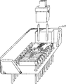
Fig. 1 a represents the preferred embodiment that this optical interconnection connects.It comprises the joints of optical fibre 150 and photoelectron plug-in card 100.
These joints of optical fibre 150 comprise the clamper 125 that has plane 130, and many optical fiber 135 are embedded in this clamper, and two guide poles 140 are slidably mounted on two in the cylinder duct 141.
These optical fiber have coupled end 131, vertically with surperficial 130 adjacency.The coupled end of this optical fiber is exposed, so that receive or the emission optical radiation.As surperficial 130 end-views are represented among Fig. 1 b, formed one-dimension optical-fiber array 132 by coupled end 131.In this fiber array, the distance between any two optical fiber equals the distance of other any two adjacent optical fiber.Preferably make the distance between any two adjacent fiber optic hubs be about 0.25mm.
Duct 141 and bar 140 relative these fiber array symmetry location, the position of its relative fiber array is determined in advance.
Photoelectron plug-in card 100 comprises semiconductor wafer 105, the one dimension photodevice matrix 110 of whole processing on this semiconductor wafer, and the many leads 115 that are used to connect these photoelectric devices.This wafer comprises two mating holes 120, approximately has the diameter identical with duct 141 to admit guide rod.The more favourable practice is that the mating holes 120 of photodevice matrix 110 and plug-in card is had basically as the 141 formed same patterns of duct on the fiber array 132 and the joints of optical fibre, and in the heart distance equates with distance between any two adjacent fiber optic hubs in the promptly any two adjacent photoelectric devices.Therefore, by allowing mating holes 120 engagements on the guide rod in the duct 140 and photoelectricity plug-in card on the joints of optical fibre, fiber array is aimed at vertically with photodevice matrix simply.Each optical fiber is also aimed at corresponding photoelectric device.
With the similar optical conenctor of optical conenctor that Fig. 1 a represents, be disclosed in people's such as Hayashi the open No.0 of european patent application, in 226,274, be referred to herein as a reference.The optical conenctor that to have two adjacent fiber optic hub tolerance limit differences be the same type of the 10 μ m orders of magnitude can have been bought from the market.
Photodevice matrix on the semiconductor wafer and mating holes are to determine by developing good semiconducter process, for example photoetching and chemistry or active-ion-etch.Thereby the tolerance of device looks or mating holes can be controlled within the 10 μ m orders of magnitude.This tolerance is combined with the close tolerance of the commercially available joints of optical fibre, and this connecting can provide good coupling efficiency, and can easily connect or disconnect.
This optical fiber can be single mode or multimode optical fiber, for example plastic optical fiber.Yet this optical fiber preferably has the multimode optical fiber of core diameter from 50 to 100 mu m ranges.Multimode optical fiber has the core diameter bigger than single-mode fiber usually, consequently can provide higher alignment tolerance than single-mode fiber.
Photoelectric device can be various types of devices, as edge emitter laser, superpower light emitting diode (SLED), vertical chamber surface-emitting laser (VCSEL), other surface light-emitting device or photodetector.They can also be the integrated devices of one or more kinds of devices of combination, for example VCSEL and transistor combination or photo-detector and transistor combination.
When photoelectric device was VCSEL, this optical interconnection connect the effect that light signal is sent to the transmitter in the optical fiber of playing.In general, alignment tolerance was in the scope of 2~20 μ m during this connected.For example the diameter of each VCSEL is about 20 μ m, and every optical fiber all is the multimode optical fiber that core diameter is about 62.5 μ m, and its alignment tolerance is about 10 μ m.
This optical interconnection connects the electronic-circuit device that further also can comprise with the VCSEL array interconnect, so that drive and modulation VCSEL.This electronic-circuit device can wholely be processed on semiconductor wafer, perhaps integrates as hydrid integrated circuit and VCSEL array.
If photoelectric device is the photodetector that forms on semiconductor wafer, then this optical interconnection connects the effect of playing receiver, with from the optical fiber receiving optical signals.For example, if each photodetector all is to have the Schottky barrier photodetector that diameter is about 100 μ m, and every optical fiber all is the multimode optical fiber with the about 62.5 μ m of core diameter, and then the alignment tolerance between optical fiber and detector is about 20 μ m.
In above preferred embodiment, the example of being lifted is an one-dimensional array.Yet also can utilize two-dimensional array similarly, connect with the optical interconnection that forms two dimension.
In the second embodiment of the present invention, this optical interconnection connects and also comprises an optical conenctor and a photoelectron plug-in card.This connector comprises a clamper, is fixed on many optical fiber and guiding mechanism in the clamper.The photoelectron plug-in card comprises a substrate, is configured in the semiconductor wafer on this substrate, and the photodevice matrix of whole processing on this semiconductor wafer.This photoelectron plug-in card further comprise processing first aligning guide on the substrate and be configured in wafer and substrate between second aligning guide so that relative first aligning guide of photodevice matrix is correctly located.By mechanically allowing the guiding mechanism of connector aim at and mesh, just the optical fiber coupling can be associated on the photodevice matrix with first aligning guide of plug-in card.
Fig. 2 a represents the preferred embodiment that this optical interconnection connects, and it comprises an optical conenctor 150 and a photoelectron plug-in card 101.For simplicity, components identical is represented with numbering same among Fig. 1 among Fig. 2 a and the 2b.The joints of optical fibre 150 in the present embodiment are identical with optical conenctor among first embodiment, thereby do not comment at this.
Photoelectron plug-in card 101 comprise an insulation substrate 90, be configured in semiconductor wafer 105 on this substrate, whole processing at the linearly aligned photodevice matrix 110 on this semiconductor wafer, be interconnected in the electronic-circuit device 117 on this photodevice matrix, and be limited to the contact pins 108 that substrate peripheral is used to connect this circuit arrangement.This photoelectron plug-in card further comprises two mating holes 119 of processing on substrate of using as first aligning guide, to admit guide pole.As representing among Fig. 2 b, this plug-in card further comprises second aligning guide 91, is formed between the first surface 96 of the second surface 95 of semiconductor wafer and substrate.Second aligning guide is along laterally allowing first aligning guide 119 that forms on photodevice matrix and the substrate aim at.
It is as follows to constitute the principle that this optical interconnection connects:
At first on semiconductor wafer, process photoelectric device.These devices are arranged to have array as the same pattern of fiber array with formation.Utilization develop good semiconductor technology, can limit the position of this photoelectric device exactly, make in any two adjacent devices distance in the heart equate with distance between any two adjacent fiber optic hubs.
Subsequent employing such as laser accurate drilling technology are determined mating holes 119 on substrate.This mating holes has the diameter same as duct in the joints of optical fibre 141 basically, and in two mating holes in the heart distance basically with two ducts between identical.Thereby guide rod herewith mating holes aim at.
Then by utilizing the upside-down mounting welding technology, along laterally photodevice matrix being aimed at this mating holes.As Fig. 2 b represents, the step that the upside-down mounting welding technology mainly comprises is: form first group of metal bond pad 93 on the first surface 96 of substrate, the relative mating holes 119 of its pattern has preposition, and this then takes place by deposition one deck scolder on substrate.Make this solder layer composition by photoetching and corrosion then, form the second set of solder pattern 94 with top at first group of metal pattern.The 3rd group of metal bond pad 92 is the direct reflection picture of the first assembly welding contact, is to be limited to subsequently on the second surface 95 of semiconductor wafer.By adopting the infrared ray technique of alignment, the 3rd picture group case is aimed at photodevice matrix according to a kind of like this mode, if thereby the 3rd picture group case is vertically aimed at the first picture group case, then photodevice matrix will laterally be aimed at mating holes by the certain way edge, thereby photodevice matrix also will vertically be aimed at fiber array.
The 3rd picture group case is aimed at the first picture group case, and the more favourable practice is by automatic Alignment Process.In automatic Alignment Process process, at first roughly the 3rd picture group case is aimed at the second picture group case.Heating is so that solder fusing then.The scolder that has melted will constrain between the 3rd and first metal pattern, and not along laterally flowing to outside this pattern.Because the effect of this solder surface tension force, the 3rd picture group case can automatically be aimed at the first picture group case.When not heating, solder cools, and also auto-alignment process is finished.This upside-down mounting welding technology is described in detail by people such as Wale in " the upside-down mounting welding makes optics intercom system (ICS) optimization " literary composition, referring to IEEE circuit and device, and 1992,11, PP.25-31 is incorporated herein by reference.
Therefore, when this flow of solder material auto-alignment process was finished, photodevice matrix was just according to the same manner lateral alignment mating holes of fiber array alignment guide bar.So,, fiber array aligning and coupling are associated on the photodevice matrix by along vertically guide pole being aimed at and meshed with mating holes.
As the optical interconnection of Fig. 1 a connect in the situation, if photoelectric device is VCSEL, and electronic-circuit device 117 was the integrated circuit that drives and modulation VCSEL is used, and then this connects and plays the effect of optical signalling being injected the optical launcher of optical fiber.If photoelectric device is a photodetector, then this connects and plays the effect of optical receiver, to receive the optical signalling that sends through optical fiber.Photodetector then will be therewith the electric signal of optical signalling correspondence send electronic-circuit device to, before it is forwarded to other circuit such as computing machine or processor, this signal is handled.If photoelectric device not only comprises VCSEL but also comprise photodetector, then this optical interconnection connect in fact be transmitter be again receiver.
Should be pointed out that by utilizing the automatic Alignment Process of flow of solder material, can make two or more a plurality of independent semiconductor wafer aim at a fiber array.In this case, the many devices on wafer are associated on some optical fiber of the joints of optical fibre by coupling, and the many devices on other wafer then coupling are associated on some other optical fiber.In this manner, transmitter and receiver can be associated on the single optical conenctor by coupling.
The optical interconnection of Fig. 3 presentation graphs 2 connects the situation that is installed in the 20 pin plug-in units 200.These joints of optical fibre can be fixed on the photoelectron plug-in card or by taking off on it at an easy rate.
Fig. 4 represents that optical interconnection of the present invention scoops out and is used for plug-in card connecting to plug-in card.In this used, plug-in card 400 was connected on the plug-in card 410 through connector 405 and 415.Fig. 4 b is for amplifying expression connector 405 or 415.Each connector 405 or 415 comprises that all an optical interconnection as Fig. 1 a or 3 expressions connects.If the optical interconnection that connector 405 only comprises as transmitter connects, and the optical interconnection that connector 415 only comprises as receiver connects, and data just can only send to plug-in card 410 from plug-in card 400 so.Yet if connector 405 and 415 boths comprise that having the optical interconnection that transmits and receives device connects, data can transmit between plug-in card through fibre ribbon according to full duplex mode so.
In the third embodiment of the present invention, optical interconnection connects the vertical-cavity surface emitting laser that comprises that the optical fiber that has coupled end and coupling join this optical fiber coupled end.
This optical fiber includes core and is looped around this core covering on every side.The fiber cores that is in the optical fiber coupled end falls in, so that form the structure of showing the edge, edge wherein is made up of covering.
Vertical-cavity surface emitting laser has second catoptron, is the reverberator of a cloth loudspeaker lattice distribution, comprises many layers that one deck forms at another layer top.More advantageously form a high platform, have diameter less than above-mentioned optical fiber edge internal diameter by many outermost layers of second catoptron.This high platform and the engagement of optical fiber coupled end are placed in this inside, edge with the essential part with high platform.The optical radiation that VCSEL sends then is coupled in the optical fiber basically entirely.
Fig. 5 a to 5c represents the preferred embodiments of the present invention.
Particularly, Fig. 5 a represent optical fiber 500 and with its coupling connection before the 3-D view of VCSEL.Optical fiber 500 includes core 505 and around the covering 510 of this core.In the coupled end 515 of optical fiber, core falls in, and mainly is the edge 516 that is made of covering to form.VCSEL then comprises some basalises of describing among a high platform 555 of being made up of many outermost layers of second catoptron, Fig. 5 b and around the joint 565 of high platform.
Fig. 5 b represents the sectional view that this optical interconnection connects.VCSEL includes the part 545 of first catoptron 525 that forms, first pad 530, active region 535, second pad 540, second catoptron on substrate 520, and the high platform part 555 of second catoptron.It further comprises around the joint 565 of high platform and the joint 575 that forms on substrate.In addition, exist a protection most surfaces to avoid the passivation layer 560 of atmospheric effect.This passivation layer is SiO preferably
2Layer.This laser instrument further comprises an annular injection current limiting layer 550 around the active region.
First and second catoptron boths are reverberators of cloth loudspeaker lattice distribution, and each catoptron comprises that all one deck is formed on many layers at another layer top.In addition, every layer all is quarter-wave thickness, and wherein said wavelength is the wavelength in this layer.High platform 555 preferably comprises dielectric layer, and layer 545 is for having the semiconductor layer of high-dopant concentration, with the low resistance contact that forms with joint 565.
The coupled end of optical fiber is securely fixed in VCSEL laser instrument top by optical resin glue 570.
Optical fiber during this connects can be single-mode fiber, multimode optical fiber or plastic optical fiber.
Fig. 5 c represents this 3-D view that connects.In this connected, all optical radiation all were coupled to basically in the optical fiber and do not need extra aligning guide.
This connecting is prepared as follows: at first prepare the VCSEL laser instrument shown in Fig. 5 b, be manufactured on the optical fiber that coupled end has recessed core subsequently.The core and the covering of glass optical fiber are made by silicon dioxide usually.Yet fiber cores will be mixed usually to improve its refractive index, then by the buffering hydrofluorite (BHF) or other acid selectively from covering etching it.Subsequent optical fiber and the VCSEL laser alignment that allows etching, and Qi Gaotai is fixed in the edge.Then optical resin glue is added on optical fiber and the laser instrument.
This connecting also can be made one dimension or two-dimensional array, and wherein integrally formed VCSEL laser array is associated on the fiber array by coupling.
Fig. 6 a and 6b represent the example that this optical interconnection connects, and the optical fiber linear array that comprises of the joints of optical fibre 650 wherein is with the linear array coupling connection of VCSEL laser instrument.Particularly, Fig. 6 a represents the fiber array before VCSEL array and the coupling connection, and Fig. 6 b then represents connecting after their couplings connection.
In the present embodiment, each VCSEL laser instrument and each optical fiber all have the same structure of describing as among Fig. 5 b, so at this it is not described in detail.In addition, can be by utilizing the mating holes of a pair of duct in the joints of optical fibre and guide rod and contiguous VCSEL laser array, as described in Fig. 1~4 embodiment, allow the joints of optical fibre 650 aim at and coupling is associated on the VCSEL laser array.
As those skilled in the art will be appreciated that, can make many changes within the scope of the invention, be not defined as that following claim limits except.
Should be pointed out that in this whole declarative procedure optical fiber can be the optical fiber of single-mode fiber, multimode optical fiber (for example plastic optical fiber) or other type; Photodevice matrix can be one dimension or two-dimentional; Photoelectric device can be edge emitter laser, high-strength light emitting diode, photodetector, the perhaps photoelectric device of other any kind.They are all within protection scope of the present invention.
Claims (66)
1. an optical interconnection connects, and includes:
Multiple fiber optical connector, it comprises: the clamper that has one first plane; Be fixed on the many optical fiber in this clamper, wherein each optical fiber all has one in abutting connection with first end on above-mentioned first plane, in order that make outside it is exposed to, receiving or the emission optical radiation, and forms a fiber array with first pattern by these optical fiber first ends; And relatively this fiber array be configured in precalculated position in the above-mentioned clamper guiding mechanism and
The photoelectron plug-in card comprises: the photodevice matrix of a whole processing on semiconductor wafer, and described photodevice matrix has the essentially identical pattern of first pattern with above-mentioned fiber array; And be formed on aligning guide on the above-mentioned wafer, and described aligning guide is as the position of the above-mentioned relatively fiber array of guiding mechanism, and being configured in above-mentioned relatively photodevice matrix is essentially identical precalculated position, and,
Above-mentioned aligning guide is admitted above-mentioned guiding mechanism, so that above-mentioned photodevice matrix is aimed at by mechanical system with above-mentioned fiber array, thereby make each photoelectric device aim at an optical fiber, and optical radiation is transmitted in the above-mentioned fiber array, or receive optical radiation by above-mentioned fiber array by described photoelectric device.
2. according to the connecting of claim 1, wherein said guiding mechanism comprises two guide rods that are installed in the clamper, and described guide rod passes above-mentioned first plane of clamper and stretches out; And described aligning guide comprises two mating holes, aims at and meshes with above-mentioned mating holes by above-mentioned guide rod, so that make fiber array aim at photodevice matrix.
3. according to the connecting of claim 2, wherein said fiber array is configured between two guide rods.
4. according to the connecting of claim 1, wherein said guiding mechanism comprises two guide rods that are installed in the clamper, and described guide rod stretches out along above-mentioned first plane that the direction of vertical above-mentioned first surface is passed clamper; And described aligning guide comprises two mating holes, aims at and meshes with above-mentioned mating holes by above-mentioned guide rod, so that make above-mentioned fiber array aim at above-mentioned photodevice matrix.
5. according to the connecting of claim 4, wherein said fiber array is configured between above-mentioned two guide rods.
6. according to the connecting of claim 1, optical fiber wherein forms one-dimensional array.
7. according to the connecting of claim 1, optical fiber wherein forms two-dimensional array.
8. according to the connecting of claim 6, photodevice matrix wherein comprises the vertical-cavity surface emitting laser of one-dimensional array, and each laser instrument is all aimed at an optical fiber vertically, and receives the optical radiation that laser instrument sends by optical fiber.
9. connecting according to Claim 8 further comprises first electronic-circuit device that is interconnected on the above-mentioned laser array, so that drive and modulate above-mentioned laser instrument.
10. connecting according to Claim 8, wherein each optical fiber is plastic optical fiber.
11. connecting according to Claim 8, wherein each optical fiber is single-mode fiber.
12. connecting according to Claim 8, wherein each optical fiber is multimode optical fiber.
13. according to connecting of claim 12, wherein each multimode optical fiber has the diameter that is about 62.5 μ m.
14. according to connecting of claim 13, wherein each vertical-cavity surface emitting laser has the diameter that is about 20 μ m.
15. according to connecting of claim 6, photodevice matrix wherein comprises the photodetector array of one dimension, each photodetector is aimed at optical fiber end vertically, and is received the optical radiation of laser instrument emission by detector.
16. according to connecting of claim 15, photodetector wherein is the Schottky barrier photodetector.
17., further comprise second electronic-circuit device that is used to receive from the electric signal of photodetector according to connecting of claim 15.
18. according to connecting of claim 16, wherein each optical fiber is multimode optical fiber.
19. according to connecting of claim 18, wherein each multimode optical fiber has the diameter of about 62.5 μ m.
20. according to connecting of claim 19, wherein each photodetector has the diameter of about 100 μ m.
21. a photoelectron connects, and includes:
Multiple fiber optical connector, it comprises: a clamper that has a plane at least; Many optical fiber that are fixed on the clamper, each optical fiber have first end in abutting connection with first surface, in order that make its exposure, receiving or to send optical radiation, and form a fiber array with first pattern by first end of above-mentioned optical fiber; And above-mentioned relatively fiber array be configured in precalculated position in the above-mentioned clamper guiding mechanism and
The photoelectron plug-in card, it comprises: the substrate with first surface and first aligning guide; The photodevice matrix of whole processing on the semiconductor wafer first surface, described photodevice matrix has the essentially identical pattern of first pattern with above-mentioned fiber array, and described wafer configuration is on this substrate; Second aligning guide is used to make above-mentioned photodevice matrix to aim at above-mentioned first aligning guide; Above-mentioned first aligning guide is as the position of the above-mentioned relatively fiber array of guiding mechanism, and being configured in above-mentioned relatively photodevice matrix is essentially identical precalculated position, and
Above-mentioned first aligning guide is admitted above-mentioned guiding mechanism, so that above-mentioned photodevice matrix is aimed at above-mentioned fiber array by mechanical system, thereby make each photoelectric device aim at an optical fiber, and optical radiation is transmitted in the above-mentioned fiber array, or receive optical radiation by above-mentioned fiber array by above-mentioned photodevice matrix.
22. according to connecting of claim 21, wherein said second aligning guide comprises and is formed on two groups of scolders between the identical metal pattern, wherein one of metal pattern is formed on the second surface of semiconductor wafer, and another metal pattern is formed on the first surface of substrate.
23. according to connecting of claim 21, wherein said guiding mechanism comprises two guide rods that are installed in the clamper, described guide rod passes above-mentioned first plane of clamper and stretches out; And described first aligning guide comprises two mating holes, aims at and meshes with above-mentioned mating holes by above-mentioned guide rod, just makes fiber array aim at photodevice matrix.
24. according to connecting of claim 23, wherein said fiber array is configured between two guide rods.
25. according to connecting of claim 21, wherein said guiding mechanism comprises two guide rods that are installed in the clamper, described guide rod stretches out along above-mentioned first plane that the direction of vertical above-mentioned first surface is passed clamper; And described aligning guide comprises two mating holes, aims at and meshes with above-mentioned mating holes by above-mentioned guide rod, just makes above-mentioned fiber array aim at above-mentioned photodevice matrix.
26. according to connecting of claim 25, wherein said fiber array is configured between two guide rods.
27. according to connecting of claim 21, optical fiber wherein forms two-dimensional array.
28. according to connecting of claim 21, optical fiber wherein forms one-dimensional array.
29. according to connecting of claim 28, optical fiber wherein is plastic optical fiber.
30. according to connecting of claim 28, optical fiber wherein is single-mode fiber.
31. according to connecting of claim 28, each optical fiber wherein is multimode optical fiber.
32. according to connecting of claim 31, multimode optical fiber wherein has the core diameter of about 62.5 μ m.
33. according to connecting of claim 32, photodevice matrix wherein comprises the vertical-cavity surface emitting laser of one-dimensional array, each laser instrument is all aimed at an end of optical fiber vertically, and receives the optical radiation that laser instrument sends by optical fiber.
34., further comprise first electronic-circuit device that is interconnected on the laser array, so that drive and modulate above-mentioned laser instrument according to connecting of claim 32.
35. according to connecting of claim 34, wherein each vertical-cavity surface emitting laser has the diameter of about 20 μ m.
36. according to connecting of claim 31, photodevice matrix wherein comprises the photodetector array of one dimension, each photodetector is aimed at optical fiber end vertically, and receives the optical radiation that laser instrument sends by detector.
37., further comprise second electronic-circuit device that is used to receive from the electric signal of above-mentioned photodetector according to connecting of claim 36.
38. according to connecting of claim 36, photodetector wherein is the Schottky barrier photodetector.
39. according to connecting of claim 36, wherein each optical fiber is multimode optical fiber.
40. according to connecting of claim 39, multimode optical fiber wherein has the diameter of about 62.5 μ m.
41. according to connecting of claim 40, wherein each photodetector has the diameter of about 100 μ m.
42. one kind is used for optical conenctor is interconnected in method on the photoelectron plug-in card, comprises the steps:
One multiple fiber optical connector is provided, and this connector comprises: a clamper that has a plane at least; Be fixed on the many optical fiber in the clamper, wherein each optical fiber has first end in abutting connection with first surface, in order that make its exposure, receiving or to send optical radiation, and forms a fiber array with first pattern by first end of this optical fiber; And this fiber array is configured in the guiding mechanism in above-mentioned clamper precalculated position relatively;
One photoelectron plug-in card is provided, and this plug-in card comprises: the photodevice matrix of a whole processing on semiconductor wafer, and described photoelectric device has the essentially identical pattern of first pattern as above-mentioned fiber array; And be formed on aligning guide on this wafer, and above-mentioned aligning guide is as the above-mentioned relatively fiber array of guiding mechanism position, and being configured in above-mentioned relatively photodevice matrix is essentially identical precalculated position, and
Allow the guiding mechanism of above-mentioned connector aim at and to mesh with the aligning guide of above-mentioned plug-in card, so that above-mentioned photodevice matrix is aimed at above-mentioned fiber array by mechanical system, thereby make each photoelectric device aim at an end of optical fiber, and optical radiation is transmitted in the above-mentioned fiber array, or receive optical radiation by this fiber array by above-mentioned photodevice matrix.
43. a method that is used for optical conenctor and the interconnection of photoelectron plug-in card comprises the steps:
One multiple fiber optical connector is provided, and this connector comprises: a clamper that has a plane at least; Be fixed on the many optical fiber in this clamper, wherein each optical fiber has first end in abutting connection with first surface, in order that make its exposure, receiving or to send optical radiation, and forms a fiber array with first pattern by above-mentioned first end of above-mentioned optical fiber; And above-mentioned relatively fiber array is configured in the guiding mechanism in above-mentioned clamper precalculated position;
One photoelectron plug-in card is provided, and this plug-in card comprises: one has the substrate of the first surface and first aligning guide; The photodevice matrix of whole processing on the semiconductor wafer first surface, described photoelectric device has the essentially identical pattern of first pattern with above-mentioned fiber array, and described wafer configuration is on this substrate; Second aligning guide is used to make above-mentioned photodevice matrix to aim at above-mentioned first aligning guide; Above-mentioned first aligning guide is as the position of the above-mentioned relatively fiber array of guiding mechanism, and being configured in above-mentioned relatively photodevice matrix is essentially identical precalculated position, and
Allow the above-mentioned guiding mechanism of above-mentioned connector aim at and to mesh with above-mentioned first aligning guide, make above-mentioned photodevice matrix aim at above-mentioned fiber array by mechanical system, thereby make each photoelectric device aim at an end of optical fiber, and optical radiation is transmitted in the above-mentioned fiber array, or receive the optical radiation that above-mentioned fiber array sends by above-mentioned photodevice matrix.
44. an optical interconnection connects, and includes:
The optical fiber of band coupled end, described optical fiber comprise core and around the covering of this core, the fiber cores that is in coupled end falls in, so that form the structure of belt edge, this edge mainly is made up of covering, and
Vertical-cavity surface emitting laser, it comprises: semiconductor chip; First catoptron that on above-mentioned substrate, forms, be positioned on first catoptron and second catoptron in parallel, it has constituted the optics cavity vertical with substrate with first catoptron, and first and second catoptron be the reverberator of cloth loudspeaker lattice distribution, the many layer that is formed on another layer top by one deck is formed; And by first and second gasket rings between above-mentioned catoptron around the active region;
Form a high platform by some outermost layers of above-mentioned second catoptron, its diameter is less than the internal diameter at above-mentioned optical fiber edge;
The structure engages at the above-mentioned demonstration edge of above-mentioned high platform and optical fiber is placed in this inside, edge with the major part with described high platform, and
The optical radiation that above-mentioned laser instrument sends is coupled in the above-mentioned optical fiber basically entirely.
45., further comprise the fixing means that is used to keep relative position between above-mentioned optical fiber coupled end and the above-mentioned laser instrument according to connecting of claim 44.
46. according to connecting of claim 45, wherein said fixing means comprises the epoxide-resin glue that is added in coupled end and laser instrument outside.
47. according to connecting of claim 44, wherein said laser instrument further comprises around Gao Tai and is formed on joint on some layers of above-mentioned second catoptron, near the active region.
48. according to connecting of claim 44, wherein said optical fiber is single-mode fiber.
49. according to connecting of claim 44, wherein said optical fiber is multimode optical fiber.
50. according to connecting of claim 44, wherein said high platform has the thickness of 1 to 3 μ m.
51. according to connecting of claim 44, wherein said laser instrument further comprises an annular injection current restricted area around the active region.
52. an optical interconnection arranged side by side connects, and includes:
The joints of optical fibre, it comprises: the clamper that has first plane; Be fixed on the many optical fiber on the above-mentioned clamper, wherein each optical fiber all has one in abutting connection with the coupled end of above-mentioned first surface, in order that make outside it is exposed to, to receive or the emission optical radiation; Above-mentioned each optical fiber all comprises a core and around the top layer of this core, the coupled end of described core is what fall in, have the structure at edge with formation, and the edge is made of the top layer basically; The coupled end formation one of above-mentioned optical fiber has the array of first pattern; With
Be integrally formed in the vertical-cavity surface emitting laser array on the semiconductor wafer, described laser array has and the essentially identical pattern of above-mentioned fiber array pattern, and each laser instrument comprises again: first catoptron that forms on above-mentioned wafer, be positioned on first catoptron and the second parallel with it catoptron, it has constituted the optics cavity vertical with wafer with first catoptron, and first and second catoptron be the reverberator of cloth loudspeaker lattice distribution, the many layer that is formed on another layer top by one deck constitutes; And by first and second gasket rings between above-mentioned catoptron around the active region;
Form a high platform by some outermost layers of above-mentioned second catoptron, its diameter is less than the internal diameter at above-mentioned optical fiber edge;
Each high platform all with optical fiber align and engagement, be placed in the inside at optical fiber edge with major part with described high platform, and
The optical radiation that each laser instrument sends all is coupled in the optical fiber basically.
53., further comprise the stationary installation that is used to keep relative position between above-mentioned fiber array coupled end and above-mentioned laser instrument according to connecting of claim 52.
54. according to connecting of claim 53, wherein said fixing means comprises the epoxide-resin glue that is added in coupled end and laser instrument outside.
55. according to connecting of claim 53, wherein each laser instrument further comprises around Gao Tai and is formed on joint above some layers of above-mentioned second catoptron, near the active region.
56. according to connecting of claim 53, wherein each optical fiber is single-mode fiber.
57. according to connecting of claim 53, wherein each optical fiber is multimode optical fiber.
58. according to connecting of claim 53, wherein each high platform has the thickness of 1 to 3 μ m.
59. according to connecting of claim 53, wherein each laser instrument further comprises the annular injection current restricted area around the active region.
60. according to connecting of claim 53, further comprise guiding mechanism that is configured in the above-mentioned clamper and the aligning guide that is formed in the above-mentioned wafer, described aligning guide is admitted described guiding mechanism, so that above-mentioned laser array is aimed at by mechanical system with above-mentioned fiber array.
61. according to connecting of claim 60, wherein said guiding mechanism comprises two guide rods that are installed in the clamper, described guide rod stretches out by the first surface of clamper; Described aligning guide comprises two mating holes that are formed in the above-mentioned wafer, by allowing above-mentioned guide rod aim at and to mesh with above-mentioned mating holes, fiber array is aimed at laser array.
62. according to connecting of claim 53, wherein said fiber array and laser array are the two-dimensional array with basic identical pattern.
63. according to connecting of claim 53, wherein said fiber array and laser array are the one-dimensional array with basic identical pattern.
64. according to connecting of claim 4, photodevice matrix wherein comprises the high-strength light emitting diode of one-dimensional array, each diode is aimed at an optical fiber vertically, and the optical radiation of being sent by the optical fiber reception diode.
65. according to connecting of claim 32, photodevice matrix wherein comprises the high-strength light emitting diode of one-dimensional array, each diode is aimed at the end of optical fiber vertically, and the optical radiation of being sent by the optical fiber reception diode.
66. according to connecting of claim 55, wherein each laser instrument further comprises the substrate joint of configuration substrate below.
Applications Claiming Priority (2)
| Application Number | Priority Date | Filing Date | Title |
|---|---|---|---|
| US08/066757 | 1993-05-24 | ||
| US08/066,757 US5420954A (en) | 1993-05-24 | 1993-05-24 | Parallel optical interconnect |
Publications (1)
| Publication Number | Publication Date |
|---|---|
| CN1139984A true CN1139984A (en) | 1997-01-08 |
Family
ID=22071502
Family Applications (1)
| Application Number | Title | Priority Date | Filing Date |
|---|---|---|---|
| CN94192730.XA Pending CN1139984A (en) | 1993-05-24 | 1994-05-23 | Interconnection optical a fibre parallel |
Country Status (7)
| Country | Link |
|---|---|
| US (2) | US5420954A (en) |
| EP (1) | EP0704069A4 (en) |
| JP (1) | JP2001503153A (en) |
| CN (1) | CN1139984A (en) |
| AU (1) | AU6964594A (en) |
| CA (1) | CA2163760A1 (en) |
| WO (1) | WO1994028448A1 (en) |
Cited By (12)
| Publication number | Priority date | Publication date | Assignee | Title |
|---|---|---|---|---|
| WO2004019095A1 (en) * | 2002-08-22 | 2004-03-04 | The Hong Kong Applied Science Technology Research Instituted Co., Ltd. | Substrate assembly for optical coupling of lasers and receivers |
| CN101341431B (en) * | 2006-03-10 | 2010-09-29 | 住友电气工业株式会社 | Method for manufacturing optical coupling component, and optical coupling component |
| CN101167005B (en) * | 2005-04-21 | 2010-10-06 | 日本电气株式会社 | Optical backplane connector, photoelectric conversion module and optical backplane |
| CN101688954B (en) * | 2007-06-22 | 2011-10-19 | 惠普开发有限公司 | Optical interconnect |
| CN103226223A (en) * | 2013-05-13 | 2013-07-31 | 洛合镭信光电科技(上海)有限公司 | Optical engine micro-packaging structure for high-speed parallel light transmitting/receiving module |
| CN103257414A (en) * | 2013-05-07 | 2013-08-21 | 苏州旭创科技有限公司 | Parallel light transmitting and receiving assembly for broadband high-speed transmission |
| CN103278894A (en) * | 2013-06-14 | 2013-09-04 | 洛合镭信光电科技(上海)有限公司 | Coupling assembly, optical fiber array module using coupling assembly and optical transceiver engine module using coupling assembly |
| CN103326772A (en) * | 2013-05-29 | 2013-09-25 | 武汉光迅科技股份有限公司 | Mini-sized array detector |
| CN103676024A (en) * | 2012-08-31 | 2014-03-26 | 鸿富锦精密工业(深圳)有限公司 | Optical fiber connector |
| CN103698864A (en) * | 2012-09-27 | 2014-04-02 | 鸿富锦精密工业(深圳)有限公司 | Optical fiber connector |
| CN103777286A (en) * | 2012-10-23 | 2014-05-07 | 鸿富锦精密工业(深圳)有限公司 | Photoelectric conversion module |
| CN103969762A (en) * | 2013-01-31 | 2014-08-06 | 鸿富锦精密工业(深圳)有限公司 | Optical communication module |
Families Citing this family (169)
| Publication number | Priority date | Publication date | Assignee | Title |
|---|---|---|---|---|
| EP0645651B1 (en) * | 1993-03-31 | 1999-06-02 | Sumitomo Electric Industries, Ltd | Optical fiber array |
| SE9402082L (en) * | 1994-06-14 | 1995-12-15 | Ericsson Telefon Ab L M | Miniature optical capsule |
| SE9403574L (en) * | 1994-10-19 | 1996-04-20 | Ericsson Telefon Ab L M | Optocomponent capsule with optical interface |
| US5631807A (en) * | 1995-01-20 | 1997-05-20 | Minnesota Mining And Manufacturing Company | Electronic circuit structure with aperture suspended component |
| SE508763C2 (en) | 1995-11-29 | 1998-11-02 | Ericsson Telefon Ab L M | Process and device for chip mounting |
| US5940562A (en) * | 1996-03-12 | 1999-08-17 | Minnesota Mining And Manufacturing Company | Stubless optoelectronic device receptacle |
| US6805493B2 (en) | 1996-03-12 | 2004-10-19 | 3M Innovative Properties Company | Optical connector assembly using partial large diameter alignment features |
| US5657409A (en) * | 1996-03-28 | 1997-08-12 | Motorola, Inc. | Optoelectric interconnect and method for interconnecting an optical fiber with an optoelectric device |
| US6005700A (en) * | 1996-06-26 | 1999-12-21 | Aironet Wireless Communications, Inc. | Computer peripheral device with detachable portion and light display |
| US5774614A (en) * | 1996-07-16 | 1998-06-30 | Gilliland; Patrick B. | Optoelectronic coupling and method of making same |
| DE69710098T2 (en) | 1996-12-31 | 2002-08-29 | Honeywell, Inc. | FLEXIBLE OPTICAL CONNECTION UNIT |
| DE19705042C1 (en) * | 1997-02-03 | 1998-07-02 | Siemens Ag | Arrangement for coupling optoelectronic elements, each with an optically sensitive surface, to assigned optical fibers |
| DE19716480B4 (en) * | 1997-04-19 | 2004-03-25 | Micronas Semiconductor Holding Ag | Method for producing a device with a cavity for receiving an optical waveguide |
| US5857049A (en) * | 1997-05-05 | 1999-01-05 | Lucent Technologies, Inc., | Precision alignment of optoelectronic devices |
| US5933558A (en) * | 1997-05-22 | 1999-08-03 | Motorola, Inc. | Optoelectronic device and method of assembly |
| GB2327276B (en) * | 1997-07-14 | 2002-02-20 | Mitel Semiconductor Ab | Optical module |
| US5913002A (en) * | 1997-12-31 | 1999-06-15 | The Whitaker Corporation | Optical coupling device for passive alignment of optoelectronic devices and fibers |
| GB2333854B (en) * | 1998-01-31 | 2002-07-31 | Mitel Semiconductor Ab | System and method for aligning optical components |
| US6085007A (en) * | 1998-02-27 | 2000-07-04 | Jiang; Ching-Long | Passive alignment member for vertical surface emitting/detecting device |
| DE19810561A1 (en) * | 1998-03-11 | 1999-09-16 | Siemens Ag | Hybrid data plug |
| US6056448A (en) * | 1998-04-16 | 2000-05-02 | Lockheed Martin Corporation | Vertical cavity surface emitting laser array packaging |
| DE19819164C1 (en) * | 1998-04-24 | 2000-02-17 | Siemens Ag | Optical data communication module |
| US6116791A (en) * | 1998-06-01 | 2000-09-12 | Motorola, Inc. | Optical coupler and method for coupling an optical fiber to an optoelectric device |
| US6453377B1 (en) * | 1998-06-16 | 2002-09-17 | Micron Technology, Inc. | Computer including optical interconnect, memory unit, and method of assembling a computer |
| US6151430A (en) * | 1998-07-08 | 2000-11-21 | Gore Enterprise Holdings, Inc. | Photonic device having an integal guide and method of manufacturing |
| EP0977064A1 (en) * | 1998-07-28 | 2000-02-02 | Interuniversitair Micro-Elektronica Centrum Vzw | a socket and a system for optoelectronic interconnection and a method of fabricating such socket and system |
| EP0977063A1 (en) | 1998-07-28 | 2000-02-02 | Interuniversitair Micro-Elektronica Centrum Vzw | A socket and a system for optoelectronic interconnection and a method of fabricating such socket and system |
| US7208725B2 (en) * | 1998-11-25 | 2007-04-24 | Rohm And Haas Electronic Materials Llc | Optoelectronic component with encapsulant |
| US20030034438A1 (en) * | 1998-11-25 | 2003-02-20 | Sherrer David W. | Optoelectronic device-optical fiber connector having micromachined pit for passive alignment of the optoelectronic device |
| US6588949B1 (en) * | 1998-12-30 | 2003-07-08 | Honeywell Inc. | Method and apparatus for hermetically sealing photonic devices |
| US6318909B1 (en) * | 1999-02-11 | 2001-11-20 | Agilent Technologies, Inc. | Integrated packaging system for optical communications devices that provides automatic alignment with optical fibers |
| US6339470B1 (en) | 1999-04-26 | 2002-01-15 | Endovasix, Inc. | Apparatus and method for aligning an energy beam |
| US7004644B1 (en) | 1999-06-29 | 2006-02-28 | Finisar Corporation | Hermetic chip-scale package for photonic devices |
| JP2001042170A (en) * | 1999-07-28 | 2001-02-16 | Canon Inc | Optical wiring device, its driving method and electronic apparatus using the device |
| US6470114B1 (en) | 1999-08-23 | 2002-10-22 | Infineon Technologies Ag | Retroreflective conductors for optical fiber interconnects |
| US6234687B1 (en) * | 1999-08-27 | 2001-05-22 | International Business Machines Corporation | Self-aligning method and interlocking assembly for attaching an optoelectronic device to a coupler |
| US6434308B1 (en) | 1999-09-03 | 2002-08-13 | Teraconnect, Inc | Optoelectronic connector system |
| US6527456B1 (en) | 1999-10-13 | 2003-03-04 | Teraconnect, Inc. | Cluster integration approach to optical transceiver arrays and fiber bundles |
| AU2119301A (en) | 1999-10-22 | 2001-05-08 | Teraconnect, Inc. | Wafer scale integration and remoted subsystems using opto-electronic transceivers |
| AU4708201A (en) | 1999-11-15 | 2001-06-25 | Teraconnect, Inc. | Active optical interconnect |
| US6583902B1 (en) | 1999-12-09 | 2003-06-24 | Alvesta, Inc. | Modular fiber-optic transceiver |
| US6788895B2 (en) | 1999-12-10 | 2004-09-07 | Altera Corporation | Security mapping and auto reconfiguration |
| US6792178B1 (en) | 2000-01-12 | 2004-09-14 | Finisar Corporation | Fiber optic header with integrated power monitor |
| US6712527B1 (en) * | 2000-01-12 | 2004-03-30 | International Business Machines Corporation | Fiber optic connections and method for using same |
| WO2003062891A1 (en) * | 2000-03-28 | 2003-07-31 | Lockheed Martin Corporation | Passive self-alignment technique for array laser transmitters andreceivers for fiber optic applications |
| US8527046B2 (en) | 2000-04-20 | 2013-09-03 | Medtronic, Inc. | MRI-compatible implantable device |
| US6614949B2 (en) | 2000-04-21 | 2003-09-02 | Teraconnect, Inc. | Precision grid standoff for optical components on opto-electronic devices |
| WO2001086696A2 (en) * | 2000-05-09 | 2001-11-15 | Teraconnect, Inc. | Self aligning optical interconnect with multiple opto-electronic devices per fiber channel |
| US6763157B1 (en) | 2000-05-09 | 2004-07-13 | Teraconnect, Inc. | Self aligning optical interconnect with multiple opto-electronic devices per fiber channel |
| US6508595B1 (en) | 2000-05-11 | 2003-01-21 | International Business Machines Corporation | Assembly of opto-electronic module with improved heat sink |
| US6619858B1 (en) | 2000-05-20 | 2003-09-16 | Sun Microsystems, Inc. | Optical interconnect |
| US6741778B1 (en) | 2000-05-23 | 2004-05-25 | International Business Machines Corporation | Optical device with chip level precision alignment |
| GB0021240D0 (en) * | 2000-08-31 | 2000-10-18 | Bookham Technology Ltd | Optical processing device |
| WO2002019003A2 (en) * | 2000-09-01 | 2002-03-07 | Lightwave Microsystems Corporation | Apparatus and method to vertically route and connect multiple optical fibers |
| US6857790B2 (en) | 2000-09-01 | 2005-02-22 | Lightwave Microsystems Corporation | Apparatus and method to vertically route and connect multiple optical fibers |
| US6542669B1 (en) * | 2000-09-21 | 2003-04-01 | International Business Machines Corporation | Enhanced coupling arrangement for an optoelectronic transducer |
| AU2002239622A1 (en) | 2000-12-13 | 2002-06-24 | Teraconnect, Inc. | An optical waveguide assembly for interfacing a two-dimensional optoelectronic array to fiber bundles |
| AU2002231027A1 (en) | 2000-12-13 | 2002-06-24 | Teraconnect, Inc. | A packaging system for two-dimensional optoelectronic arrays |
| AU2002231207A1 (en) * | 2000-12-21 | 2002-07-01 | Biovalve Technologies, Inc. | Microneedle array systems |
| US7021836B2 (en) | 2000-12-26 | 2006-04-04 | Emcore Corporation | Attenuator and conditioner |
| US6863444B2 (en) * | 2000-12-26 | 2005-03-08 | Emcore Corporation | Housing and mounting structure |
| US6799902B2 (en) * | 2000-12-26 | 2004-10-05 | Emcore Corporation | Optoelectronic mounting structure |
| US6867377B2 (en) * | 2000-12-26 | 2005-03-15 | Emcore Corporation | Apparatus and method of using flexible printed circuit board in optical transceiver device |
| US6527457B2 (en) | 2001-02-01 | 2003-03-04 | International Business Machines Corporation | Optical fiber guide module and a method for making the same |
| US20020116029A1 (en) * | 2001-02-20 | 2002-08-22 | Victor Miller | MRI-compatible pacemaker with power carrying photonic catheter and isolated pulse generating electronics providing VOO functionality |
| US6829509B1 (en) | 2001-02-20 | 2004-12-07 | Biophan Technologies, Inc. | Electromagnetic interference immune tissue invasive system |
| US7101091B2 (en) * | 2001-02-21 | 2006-09-05 | Zarlink Semiconductor, Inc. | Apparatus for coupling a fiber optic cable to an optoelectronic device, a system including the apparatus, and a method of forming the same |
| US6724961B2 (en) * | 2002-02-14 | 2004-04-20 | Corona Optical Systems, Inc. | Method to assemble optical components to a substrate |
| GB2373064A (en) * | 2001-03-10 | 2002-09-11 | Mitel Corp | Optical fibre connector using transparent filler material |
| GB2373633B (en) * | 2001-03-20 | 2005-02-02 | Mitel Semiconductor Ab | Optical carrier |
| US6804770B2 (en) | 2001-03-22 | 2004-10-12 | International Business Machines Corporation | Method and apparatus for using past history to avoid flush conditions in a microprocessor |
| CA2445971A1 (en) * | 2001-05-01 | 2002-11-07 | Corona Optical Systems, Inc. | Alignment apertures in an optically transparent substrate |
| US6910812B2 (en) * | 2001-05-15 | 2005-06-28 | Peregrine Semiconductor Corporation | Small-scale optoelectronic package |
| WO2002095471A1 (en) * | 2001-05-24 | 2002-11-28 | Sun Microsystems, Inc. | Optical interconnect |
| DE10134637A1 (en) * | 2001-07-17 | 2003-03-27 | Harting Elektrooptische Bauteile Gmbh & Co Kg | Substrate for an opto-electronic assembly |
| WO2003012511A1 (en) * | 2001-08-01 | 2003-02-13 | Infineon Technologies Ag | Optical coupling unit and method for inserting optical wave guides into an optical coupling unit |
| US7054686B2 (en) * | 2001-08-30 | 2006-05-30 | Biophan Technologies, Inc. | Pulsewidth electrical stimulation |
| US6731979B2 (en) | 2001-08-30 | 2004-05-04 | Biophan Technologies Inc. | Pulse width cardiac pacing apparatus |
| US7446261B2 (en) | 2001-09-06 | 2008-11-04 | Finisar Corporation | Flexible circuit boards with tooling cutouts for optoelectronic modules |
| US7439449B1 (en) | 2002-02-14 | 2008-10-21 | Finisar Corporation | Flexible circuit for establishing electrical connectivity with optical subassembly |
| WO2003037399A2 (en) * | 2001-10-31 | 2003-05-08 | Biophan Technologies, Inc. | Hermetic component housing for photonic catheter |
| DE10157201A1 (en) * | 2001-11-22 | 2003-06-26 | Harting Electro Optics Gmbh & | Optoelectronic assembly |
| US7212599B2 (en) * | 2002-01-25 | 2007-05-01 | Applied Micro Circuits Corporation | Jitter and wander reduction apparatus |
| US6682228B2 (en) | 2002-02-19 | 2004-01-27 | Emcore Corporation | Connector housing for fiber-optic module |
| US6816642B1 (en) * | 2002-03-01 | 2004-11-09 | Optical Communication Products, Inc. | Apparatus and methods for using fiber optic arrays in optical communication systems |
| JP2003258273A (en) * | 2002-03-05 | 2003-09-12 | Sumitomo Electric Ind Ltd | Optical link module and optical link module board |
| US6711440B2 (en) | 2002-04-11 | 2004-03-23 | Biophan Technologies, Inc. | MRI-compatible medical device with passive generation of optical sensing signals |
| US6725092B2 (en) | 2002-04-25 | 2004-04-20 | Biophan Technologies, Inc. | Electromagnetic radiation immune medical assist device adapter |
| KR100461157B1 (en) * | 2002-06-07 | 2004-12-13 | 한국전자통신연구원 | Parallel optical interconnect module and method for manufacturing thereof |
| US6925322B2 (en) * | 2002-07-25 | 2005-08-02 | Biophan Technologies, Inc. | Optical MRI catheter system |
| KR20040022675A (en) * | 2002-09-09 | 2004-03-16 | 주식회사 아이텍 테크널러지 | Optical Transceiver With VCSEL Transmitter And Receiver Array Modules For High Speed Parallel Communications On The Optical Backplane |
| US6819813B2 (en) * | 2002-09-11 | 2004-11-16 | International Business Machines Corporation | Optical land grid array interposer |
| US7039263B2 (en) * | 2002-09-24 | 2006-05-02 | Intel Corporation | Electrooptic assembly |
| US6793407B2 (en) * | 2002-09-25 | 2004-09-21 | International Business Machines Corporation | Manufacturable optical connection assemblies |
| EP1576355A2 (en) * | 2002-09-30 | 2005-09-21 | Applied Materials Israel Ltd. | Illumination system for optical inspection |
| US7526207B2 (en) * | 2002-10-18 | 2009-04-28 | Finisar Corporation | Flexible circuit design for improved laser bias connections to optical subassemblies |
| US6960031B2 (en) * | 2002-12-19 | 2005-11-01 | Primarion, Inc. | Apparatus and method of packaging two dimensional photonic array devices |
| US6863453B2 (en) * | 2003-01-28 | 2005-03-08 | Emcore Corporation | Method and apparatus for parallel optical transceiver module assembly |
| US7150569B2 (en) * | 2003-02-24 | 2006-12-19 | Nor Spark Plug Co., Ltd. | Optical device mounted substrate assembly |
| US6856905B2 (en) * | 2003-04-29 | 2005-02-15 | Garmin At, Inc. | Systems and methods for fault detection and exclusion in navigational systems |
| US6963119B2 (en) * | 2003-05-30 | 2005-11-08 | International Business Machines Corporation | Integrated optical transducer assembly |
| NL1024108C2 (en) * | 2003-08-14 | 2005-02-15 | Framatome Connectors Int | Optical board connector assembly. |
| US7499614B2 (en) * | 2003-10-24 | 2009-03-03 | International Business Machines Corporation | Passive alignment of VCSELs to waveguides in opto-electronic cards and printed circuit boards |
| US7347632B2 (en) * | 2003-12-12 | 2008-03-25 | Mina Farr | Optical connectors for electronic devices |
| KR100583646B1 (en) * | 2003-12-24 | 2006-05-26 | 한국전자통신연구원 | Connection apparatus for parallel optical interconnect module and parallel optical interconnect module Using the same |
| US7425135B2 (en) * | 2004-04-30 | 2008-09-16 | Finisar Corporation | Flex circuit assembly |
| US7275937B2 (en) | 2004-04-30 | 2007-10-02 | Finisar Corporation | Optoelectronic module with components mounted on a flexible circuit |
| US7311240B2 (en) | 2004-04-30 | 2007-12-25 | Finisar Corporation | Electrical circuits with button plated contacts and assembly methods |
| US7656673B1 (en) * | 2004-05-25 | 2010-02-02 | University Of South Florida | Wireless micro-electro-opto-fluidic-mechanical foldable flex system |
| US7629537B2 (en) * | 2004-07-09 | 2009-12-08 | Finisar Corporation | Single layer flex circuit |
| US7809278B2 (en) * | 2004-07-26 | 2010-10-05 | Hewlett-Packard Development Company, L.P. | Apparatus and method of providing separate control and data channels between arrays of light emitters and detectors for optical communication and alignment |
| US7623793B2 (en) * | 2004-08-10 | 2009-11-24 | Hewlett-Packard Development Company, L.P. | System and method of configuring fiber optic communication channels between arrays of emitters and detectors |
| US7623783B2 (en) * | 2004-08-10 | 2009-11-24 | Hewlett-Packard Development Company, L.P. | System and method of self-configuring optical communication channels between arrays of emitters and detectors |
| US7251388B2 (en) * | 2004-08-10 | 2007-07-31 | Hewlett-Packard Development Company, L.P. | Apparatus for providing optical communication between integrated circuits of different PC boards and an integrated circuit assembly for use therein |
| US7269321B2 (en) * | 2004-08-10 | 2007-09-11 | Hewlett-Packard Development Company, L.P. | System and method of configuring fiber optic communication channels between arrays of emitters and detectors |
| US7653108B2 (en) * | 2004-09-09 | 2010-01-26 | Hewlett-Packard Development Company, L.P. | Apparatus and method of establishing optical communication channels between a steerable array of laser emitters and an array of optical detectors |
| US7229218B2 (en) * | 2004-09-20 | 2007-06-12 | Hewlett-Packard Development Company, L.P. | Apparatus and method of providing an optical connection between PC boards for optical communication |
| US7548675B2 (en) | 2004-09-29 | 2009-06-16 | Finisar Corporation | Optical cables for consumer electronics |
| US7706692B2 (en) | 2004-09-29 | 2010-04-27 | Finisar Corporation | Consumer electronics with optical communication interface |
| US8412052B2 (en) | 2004-10-22 | 2013-04-02 | Intel Corporation | Surface mount (SMT) connector for VCSEL and photodiode arrays |
| US7657940B2 (en) * | 2004-10-28 | 2010-02-02 | Cisco Technology, Inc. | System for SSL re-encryption after load balance |
| US7344315B2 (en) * | 2004-11-03 | 2008-03-18 | Hewlett-Packard Development Company, L.P. | Optical connections and methods of forming optical connections |
| US7400790B2 (en) * | 2004-11-03 | 2008-07-15 | Hewlett-Packard Development Company, L.P. | Optical connections and methods of forming optical connections |
| US20060093271A1 (en) * | 2004-11-03 | 2006-05-04 | Fenwick David M | Optical connections and methods of forming optical connections |
| US7118285B2 (en) * | 2004-11-03 | 2006-10-10 | Hewlett-Packard Development Company, L.P. | Optical connections and methods of forming optical connections |
| JP4705432B2 (en) * | 2005-03-28 | 2011-06-22 | 富士通コンポーネント株式会社 | connector |
| US20060228076A1 (en) * | 2005-03-30 | 2006-10-12 | Xerox Corporation | Parallel optical interface |
| US7703991B2 (en) * | 2005-05-06 | 2010-04-27 | Intel Corporation | Flip-chip mountable optical connector for chip-to-chip optical interconnectability |
| US7331819B2 (en) * | 2005-07-11 | 2008-02-19 | Finisar Corporation | Media converter |
| US7729618B2 (en) | 2005-08-30 | 2010-06-01 | Finisar Corporation | Optical networks for consumer electronics |
| US7860398B2 (en) | 2005-09-15 | 2010-12-28 | Finisar Corporation | Laser drivers for closed path optical cables |
| TW200737628A (en) * | 2005-11-14 | 2007-10-01 | Applied Materials Inc | Semiconductor laser |
| JP2007187742A (en) | 2006-01-11 | 2007-07-26 | Fuji Xerox Co Ltd | Optical connector and substrate |
| US7499616B2 (en) * | 2006-04-10 | 2009-03-03 | Finisar Corporation | Active optical cable with electrical connector |
| US7445389B2 (en) * | 2006-04-10 | 2008-11-04 | Finisar Corporation | Active optical cable with integrated eye safety |
| US7712976B2 (en) | 2006-04-10 | 2010-05-11 | Finisar Corporation | Active optical cable with integrated retiming |
| US7778510B2 (en) * | 2006-04-10 | 2010-08-17 | Finisar Corporation | Active optical cable electrical connector |
| US7876989B2 (en) * | 2006-04-10 | 2011-01-25 | Finisar Corporation | Active optical cable with integrated power |
| US8083417B2 (en) * | 2006-04-10 | 2011-12-27 | Finisar Corporation | Active optical cable electrical adaptor |
| US7401985B2 (en) * | 2006-04-10 | 2008-07-22 | Finisar Corporation | Electrical-optical active optical cable |
| US9250399B2 (en) * | 2006-08-31 | 2016-02-02 | Optogig, Inc. | High density active modular optoelectronic device for use with push-release mechanism and method for using same |
| US8769171B2 (en) * | 2007-04-06 | 2014-07-01 | Finisar Corporation | Electrical device with electrical interface that is compatible with integrated optical cable receptacle |
| US8244124B2 (en) | 2007-04-30 | 2012-08-14 | Finisar Corporation | Eye safety mechanism for use in optical cable with electrical interfaces |
| JP4819000B2 (en) * | 2007-07-11 | 2011-11-16 | 富士通コンポーネント株式会社 | Optical waveguide holding member and optical transceiver |
| US8746989B2 (en) * | 2007-10-15 | 2014-06-10 | Hewlett-Packard Development Company, L.P. | Board to board optical interconnect using an optical interconnect assembly |
| EP2517058B1 (en) | 2009-12-21 | 2020-07-15 | Hewlett-Packard Enterprise Development LP | Circuit switched optical interconnection fabric |
| WO2011084155A1 (en) | 2010-01-06 | 2011-07-14 | Hewlett-Packard Development Company, L.P. | Optical interconnect |
| TW201211606A (en) * | 2010-09-03 | 2012-03-16 | Univ Nat Central | Optical transmission module with optical waveguide structure |
| US8585300B2 (en) * | 2011-02-09 | 2013-11-19 | Tyco Electronics Nederland Bv | Ferrule with alignment pin channels |
| US9002155B2 (en) * | 2011-03-28 | 2015-04-07 | Altera Corporation | Integrated optical-electronic interface in programmable integrated circuit device |
| JP2012234025A (en) * | 2011-04-28 | 2012-11-29 | Nitto Denko Corp | Opto-electric hybrid substrate and manufacturing method of the same |
| JP5852736B2 (en) | 2011-07-29 | 2016-02-03 | モレックス エルエルシー | Multi-fiber ferrule with lens plate |
| US8834041B2 (en) | 2011-09-29 | 2014-09-16 | Corning Cable Systems Llc | Ferrule-based optical component assemblies |
| US8954712B2 (en) * | 2011-12-07 | 2015-02-10 | International Business Machines Corporation | Computer system including an all-to-all communication network of processors connected using electrical and optical links |
| US10215926B2 (en) | 2011-12-14 | 2019-02-26 | Commscope Technologies Llc | Multi-fiber fiber optic connection system with flexible, insertable pins |
| JP6133028B2 (en) * | 2012-09-07 | 2017-05-24 | 古河電気工業株式会社 | Optical fiber, optical module, and optical module manufacturing method |
| US9250404B2 (en) * | 2012-11-23 | 2016-02-02 | Electronics And Telecommunications Research Institute | Multi-channel optical module and manufacturing method of the same |
| US9134490B2 (en) * | 2012-12-06 | 2015-09-15 | Laxense Inc. | Passive alignment multichannel parallel optical system |
| KR101999199B1 (en) * | 2013-03-12 | 2019-07-11 | 삼성전자주식회사 | Optical package |
| GB2525657B (en) | 2014-05-01 | 2018-01-31 | Xyratex Tech Limited | An optical connector assembly, an optical printed circuit board assembly, an insert, and a method of manufacturing an optical connector assembly |
| JP6379642B2 (en) * | 2014-05-07 | 2018-08-29 | 住友電気工業株式会社 | Optical device manufacturing method, optical device, and optical connector unit |
| JP6299481B2 (en) * | 2014-06-24 | 2018-03-28 | ソニー株式会社 | Optical transmitter, optical receiver, optical cable, and optical transmission method |
| JP6299480B2 (en) * | 2014-06-24 | 2018-03-28 | ソニー株式会社 | Optical transmitter, optical receiver, optical cable, and optical transmission method |
| EP3227736A1 (en) | 2014-12-01 | 2017-10-11 | Commscope Asia Holdings B.V. | Multi-fiber optic connector with pivotally-aligned ferrule |
| US10222566B1 (en) * | 2015-01-08 | 2019-03-05 | Acacia Communications, Inc. | Optoelectronic package with pluggable fiber assembly |
| US10976508B2 (en) * | 2015-01-30 | 2021-04-13 | Hewlett Packard Enterprise Development Lp | Optical modules |
| WO2016205201A1 (en) | 2015-06-19 | 2016-12-22 | Commscope Technologies Llc | Fiber optic connector ferrule with improved alignment mechanism |
| US10151888B2 (en) * | 2017-03-29 | 2018-12-11 | Mellanox Technologies, Ltd. | Optical waveguide structure |
| WO2020235041A1 (en) * | 2019-05-22 | 2020-11-26 | 日本電信電話株式会社 | Waveguide connection structure, waveguide chip, connector, method for manufacturing waveguide connection component, and method for connecting wavegude |
Family Cites Families (18)
| Publication number | Priority date | Publication date | Assignee | Title |
|---|---|---|---|---|
| US4079404A (en) * | 1976-12-30 | 1978-03-14 | International Business Machines Corporation | Self-aligning support structure for optical components |
| EP0226274A3 (en) * | 1985-11-29 | 1989-09-06 | The Furukawa Electric Co., Ltd. | Multicore optical fiber with optical connectors |
| EP0274446B1 (en) * | 1987-01-09 | 1993-08-04 | The Furukawa Electric Co., Ltd. | Method and apparatus for switching optical connector |
| US4870637A (en) * | 1987-12-24 | 1989-09-26 | American Telephone And Telegraph Company | Optical backplane |
| US4973127A (en) * | 1989-05-31 | 1990-11-27 | At&T Bell Laboratories | Multifiber optical connector and method of making same |
| JPH03132608A (en) * | 1989-10-18 | 1991-06-06 | Adamando Kogyo Kk | Multiferrule body structure |
| US5037173A (en) * | 1989-11-22 | 1991-08-06 | Texas Instruments Incorporated | Optical interconnection network |
| DE4004053A1 (en) * | 1990-02-10 | 1991-08-14 | Standard Elektrik Lorenz Ag | INTEGRATED OPTICAL RECEIVER AND / OR TRANSMITTER |
| GB9014639D0 (en) * | 1990-07-02 | 1990-08-22 | British Telecomm | Optical component packaging |
| US5155784A (en) * | 1990-11-07 | 1992-10-13 | Bicc Plc | Optical connection to backplanes |
| US5155786A (en) * | 1991-04-29 | 1992-10-13 | International Business Machines Corporation | Apparatus and a method for an optical fiber interface |
| US5168537A (en) * | 1991-06-28 | 1992-12-01 | Digital Equipment Corporation | Method and apparatus for coupling light between an optoelectronic device and a waveguide |
| US5212754A (en) * | 1991-12-27 | 1993-05-18 | At&T Bell Laboratories | Optical laser connector |
| US5230030A (en) * | 1992-04-24 | 1993-07-20 | Motorola, Inc. | Interface coupling electronic circuitry |
| US5249245A (en) * | 1992-08-31 | 1993-09-28 | Motorola, Inc. | Optoelectroinc mount including flexible substrate and method for making same |
| US5337398A (en) * | 1992-11-30 | 1994-08-09 | At&T Bell Laboratories | Single in-line optical package |
| US5309537A (en) * | 1993-04-05 | 1994-05-03 | Motorola, Inc. | Optoelectronic coupling device and method of making |
| US5337391A (en) * | 1993-05-03 | 1994-08-09 | Motorola, Inc. | Optoelectronic sub-module and method of making same |
-
1993
- 1993-05-24 US US08/066,757 patent/US5420954A/en not_active Expired - Lifetime
-
1994
- 1994-05-23 EP EP94918079A patent/EP0704069A4/en not_active Withdrawn
- 1994-05-23 JP JP07500852A patent/JP2001503153A/en not_active Ceased
- 1994-05-23 CN CN94192730.XA patent/CN1139984A/en active Pending
- 1994-05-23 AU AU69645/94A patent/AU6964594A/en not_active Abandoned
- 1994-05-23 WO PCT/US1994/005749 patent/WO1994028448A1/en not_active Application Discontinuation
- 1994-05-23 CA CA002163760A patent/CA2163760A1/en not_active Abandoned
-
1996
- 1996-06-21 US US08/667,367 patent/US5631988A/en not_active Expired - Lifetime
Cited By (16)
| Publication number | Priority date | Publication date | Assignee | Title |
|---|---|---|---|---|
| CN100412590C (en) * | 2002-08-22 | 2008-08-20 | 新科实业有限公司 | Substrate assembly for optical coupling of lasers and receivers |
| WO2004019095A1 (en) * | 2002-08-22 | 2004-03-04 | The Hong Kong Applied Science Technology Research Instituted Co., Ltd. | Substrate assembly for optical coupling of lasers and receivers |
| CN101167005B (en) * | 2005-04-21 | 2010-10-06 | 日本电气株式会社 | Optical backplane connector, photoelectric conversion module and optical backplane |
| CN101341431B (en) * | 2006-03-10 | 2010-09-29 | 住友电气工业株式会社 | Method for manufacturing optical coupling component, and optical coupling component |
| CN101688954B (en) * | 2007-06-22 | 2011-10-19 | 惠普开发有限公司 | Optical interconnect |
| CN103676024A (en) * | 2012-08-31 | 2014-03-26 | 鸿富锦精密工业(深圳)有限公司 | Optical fiber connector |
| CN103698864B (en) * | 2012-09-27 | 2016-12-07 | 鸿富锦精密工业(深圳)有限公司 | The joints of optical fibre |
| CN103698864A (en) * | 2012-09-27 | 2014-04-02 | 鸿富锦精密工业(深圳)有限公司 | Optical fiber connector |
| CN103777286A (en) * | 2012-10-23 | 2014-05-07 | 鸿富锦精密工业(深圳)有限公司 | Photoelectric conversion module |
| CN103969762A (en) * | 2013-01-31 | 2014-08-06 | 鸿富锦精密工业(深圳)有限公司 | Optical communication module |
| CN103257414A (en) * | 2013-05-07 | 2013-08-21 | 苏州旭创科技有限公司 | Parallel light transmitting and receiving assembly for broadband high-speed transmission |
| CN103257414B (en) * | 2013-05-07 | 2015-08-12 | 苏州旭创科技有限公司 | For the parallel light transceiver component of broadband high-speed transmission |
| CN103226223A (en) * | 2013-05-13 | 2013-07-31 | 洛合镭信光电科技(上海)有限公司 | Optical engine micro-packaging structure for high-speed parallel light transmitting/receiving module |
| CN103326772A (en) * | 2013-05-29 | 2013-09-25 | 武汉光迅科技股份有限公司 | Mini-sized array detector |
| CN103326772B (en) * | 2013-05-29 | 2016-09-14 | 武汉光迅科技股份有限公司 | A kind of miniaturization detector array |
| CN103278894A (en) * | 2013-06-14 | 2013-09-04 | 洛合镭信光电科技(上海)有限公司 | Coupling assembly, optical fiber array module using coupling assembly and optical transceiver engine module using coupling assembly |
Also Published As
| Publication number | Publication date |
|---|---|
| EP0704069A4 (en) | 1996-05-29 |
| JP2001503153A (en) | 2001-03-06 |
| AU6964594A (en) | 1994-12-20 |
| WO1994028448A1 (en) | 1994-12-08 |
| US5420954A (en) | 1995-05-30 |
| CA2163760A1 (en) | 1994-12-08 |
| EP0704069A1 (en) | 1996-04-03 |
| US5631988A (en) | 1997-05-20 |
Similar Documents
| Publication | Publication Date | Title |
|---|---|---|
| CN1139984A (en) | Interconnection optical a fibre parallel | |
| US7418163B2 (en) | Optoelectrical package | |
| US6850658B2 (en) | Apparatus for coupling an optoelectronic device to a fiber optic cable and a microelectronic device, a system including the apparatus, and a method of forming the same | |
| US10268006B2 (en) | Alignment mechanism of optical interconnect structure | |
| EP2581776A1 (en) | Optical connector with alignment element, optical unit and assembly method | |
| US20120014639A1 (en) | Packaged multicore fiber optical transceiver module | |
| JP2011151402A (en) | Surface mount (smt) connector for vcsel and photodiode array | |
| CN106256055A (en) | Optical-electric module and optical element | |
| US9246592B2 (en) | Structured substrate for optical fiber alignment | |
| US9014519B2 (en) | Optoelectronic interface | |
| US6786651B2 (en) | Optical interconnect structure, system and transceiver including the structure, and method of forming the same | |
| Ishii et al. | SMT-compatible optical-I/O chip packaging for chip-level optical interconnects | |
| TW200405036A (en) | Manufacturable optical connection assemblies | |
| US6434308B1 (en) | Optoelectronic connector system | |
| CN1507065A (en) | Optical transmitter receiver | |
| TWI402549B (en) | Optoelectric interconnection module | |
| Hwang et al. | Two-dimensional optical interconnection based on two-layered optical printed circuit board | |
| US7325981B2 (en) | Optical module, mounting method of the same and optical system having optical module mounted on substrate | |
| Suzuki et al. | Low-cost optical subassembly using VCSEL pre-self-aligned with optical fiber for optical interconnect applications | |
| Hiramatsu et al. | Three-dimensional waveguide arrays for coupling between fiber-optic connectors and surface-mounted optoelectronic devices | |
| Hiramatsu et al. | Optical backplane connectors using three-dimensional waveguide arrays | |
| Goulet et al. | Simple integration technique to realize parallel optical interconnects: implementation of a pluggable two-dimensional optical data link | |
| CN103376514A (en) | Optical fiber connector | |
| JP2004086157A (en) | Optical tranceiver and its manufacturing method | |
| WO2002077691A2 (en) | Optical interconnect structure, system and transceiver including the structure, and method of forming the same |
Legal Events
| Date | Code | Title | Description |
|---|---|---|---|
| C06 | Publication | ||
| PB01 | Publication | ||
| C10 | Entry into substantive examination | ||
| SE01 | Entry into force of request for substantive examination | ||
| C01 | Deemed withdrawal of patent application (patent law 1993) | ||
| WD01 | Invention patent application deemed withdrawn after publication |