CN102637679A - 半导体模块 - Google Patents
半导体模块 Download PDFInfo
- Publication number
- CN102637679A CN102637679A CN201110453505XA CN201110453505A CN102637679A CN 102637679 A CN102637679 A CN 102637679A CN 201110453505X A CN201110453505X A CN 201110453505XA CN 201110453505 A CN201110453505 A CN 201110453505A CN 102637679 A CN102637679 A CN 102637679A
- Authority
- CN
- China
- Prior art keywords
- diode
- switch element
- housing
- lead frame
- semiconductor module
- Prior art date
- Legal status (The legal status is an assumption and is not a legal conclusion. Google has not performed a legal analysis and makes no representation as to the accuracy of the status listed.)
- Pending
Links
Images

Classifications
-
- H—ELECTRICITY
- H02—GENERATION; CONVERSION OR DISTRIBUTION OF ELECTRIC POWER
- H02M—APPARATUS FOR CONVERSION BETWEEN AC AND AC, BETWEEN AC AND DC, OR BETWEEN DC AND DC, AND FOR USE WITH MAINS OR SIMILAR POWER SUPPLY SYSTEMS; CONVERSION OF DC OR AC INPUT POWER INTO SURGE OUTPUT POWER; CONTROL OR REGULATION THEREOF
- H02M7/00—Conversion of ac power input into dc power output; Conversion of dc power input into ac power output
- H02M7/02—Conversion of ac power input into dc power output without possibility of reversal
- H02M7/04—Conversion of ac power input into dc power output without possibility of reversal by static converters
- H02M7/12—Conversion of ac power input into dc power output without possibility of reversal by static converters using discharge tubes with control electrode or semiconductor devices with control electrode
- H02M7/21—Conversion of ac power input into dc power output without possibility of reversal by static converters using discharge tubes with control electrode or semiconductor devices with control electrode using devices of a triode or transistor type requiring continuous application of a control signal
- H02M7/217—Conversion of ac power input into dc power output without possibility of reversal by static converters using discharge tubes with control electrode or semiconductor devices with control electrode using devices of a triode or transistor type requiring continuous application of a control signal using semiconductor devices only
-
- H—ELECTRICITY
- H01—ELECTRIC ELEMENTS
- H01L—SEMICONDUCTOR DEVICES NOT COVERED BY CLASS H10
- H01L23/00—Details of semiconductor or other solid state devices
- H01L23/48—Arrangements for conducting electric current to or from the solid state body in operation, e.g. leads, terminal arrangements ; Selection of materials therefor
- H01L23/488—Arrangements for conducting electric current to or from the solid state body in operation, e.g. leads, terminal arrangements ; Selection of materials therefor consisting of soldered or bonded constructions
- H01L23/495—Lead-frames or other flat leads
- H01L23/49537—Plurality of lead frames mounted in one device
-
- H—ELECTRICITY
- H01—ELECTRIC ELEMENTS
- H01L—SEMICONDUCTOR DEVICES NOT COVERED BY CLASS H10
- H01L23/00—Details of semiconductor or other solid state devices
- H01L23/48—Arrangements for conducting electric current to or from the solid state body in operation, e.g. leads, terminal arrangements ; Selection of materials therefor
- H01L23/488—Arrangements for conducting electric current to or from the solid state body in operation, e.g. leads, terminal arrangements ; Selection of materials therefor consisting of soldered or bonded constructions
- H01L23/495—Lead-frames or other flat leads
- H01L23/49541—Geometry of the lead-frame
- H01L23/49548—Cross section geometry
- H01L23/49551—Cross section geometry characterised by bent parts
-
- H—ELECTRICITY
- H01—ELECTRIC ELEMENTS
- H01L—SEMICONDUCTOR DEVICES NOT COVERED BY CLASS H10
- H01L23/00—Details of semiconductor or other solid state devices
- H01L23/48—Arrangements for conducting electric current to or from the solid state body in operation, e.g. leads, terminal arrangements ; Selection of materials therefor
- H01L23/488—Arrangements for conducting electric current to or from the solid state body in operation, e.g. leads, terminal arrangements ; Selection of materials therefor consisting of soldered or bonded constructions
- H01L23/495—Lead-frames or other flat leads
- H01L23/49575—Assemblies of semiconductor devices on lead frames
-
- H—ELECTRICITY
- H01—ELECTRIC ELEMENTS
- H01L—SEMICONDUCTOR DEVICES NOT COVERED BY CLASS H10
- H01L2224/00—Indexing scheme for arrangements for connecting or disconnecting semiconductor or solid-state bodies and methods related thereto as covered by H01L24/00
- H01L2224/01—Means for bonding being attached to, or being formed on, the surface to be connected, e.g. chip-to-package, die-attach, "first-level" interconnects; Manufacturing methods related thereto
- H01L2224/26—Layer connectors, e.g. plate connectors, solder or adhesive layers; Manufacturing methods related thereto
- H01L2224/31—Structure, shape, material or disposition of the layer connectors after the connecting process
- H01L2224/32—Structure, shape, material or disposition of the layer connectors after the connecting process of an individual layer connector
- H01L2224/321—Disposition
- H01L2224/32151—Disposition the layer connector connecting between a semiconductor or solid-state body and an item not being a semiconductor or solid-state body, e.g. chip-to-substrate, chip-to-passive
- H01L2224/32221—Disposition the layer connector connecting between a semiconductor or solid-state body and an item not being a semiconductor or solid-state body, e.g. chip-to-substrate, chip-to-passive the body and the item being stacked
- H01L2224/32245—Disposition the layer connector connecting between a semiconductor or solid-state body and an item not being a semiconductor or solid-state body, e.g. chip-to-substrate, chip-to-passive the body and the item being stacked the item being metallic
-
- H—ELECTRICITY
- H01—ELECTRIC ELEMENTS
- H01L—SEMICONDUCTOR DEVICES NOT COVERED BY CLASS H10
- H01L2224/00—Indexing scheme for arrangements for connecting or disconnecting semiconductor or solid-state bodies and methods related thereto as covered by H01L24/00
- H01L2224/01—Means for bonding being attached to, or being formed on, the surface to be connected, e.g. chip-to-package, die-attach, "first-level" interconnects; Manufacturing methods related thereto
- H01L2224/42—Wire connectors; Manufacturing methods related thereto
- H01L2224/47—Structure, shape, material or disposition of the wire connectors after the connecting process
- H01L2224/48—Structure, shape, material or disposition of the wire connectors after the connecting process of an individual wire connector
- H01L2224/481—Disposition
- H01L2224/48151—Connecting between a semiconductor or solid-state body and an item not being a semiconductor or solid-state body, e.g. chip-to-substrate, chip-to-passive
- H01L2224/48221—Connecting between a semiconductor or solid-state body and an item not being a semiconductor or solid-state body, e.g. chip-to-substrate, chip-to-passive the body and the item being stacked
- H01L2224/48245—Connecting between a semiconductor or solid-state body and an item not being a semiconductor or solid-state body, e.g. chip-to-substrate, chip-to-passive the body and the item being stacked the item being metallic
- H01L2224/48247—Connecting between a semiconductor or solid-state body and an item not being a semiconductor or solid-state body, e.g. chip-to-substrate, chip-to-passive the body and the item being stacked the item being metallic connecting the wire to a bond pad of the item
-
- H—ELECTRICITY
- H01—ELECTRIC ELEMENTS
- H01L—SEMICONDUCTOR DEVICES NOT COVERED BY CLASS H10
- H01L2224/00—Indexing scheme for arrangements for connecting or disconnecting semiconductor or solid-state bodies and methods related thereto as covered by H01L24/00
- H01L2224/73—Means for bonding being of different types provided for in two or more of groups H01L2224/10, H01L2224/18, H01L2224/26, H01L2224/34, H01L2224/42, H01L2224/50, H01L2224/63, H01L2224/71
- H01L2224/732—Location after the connecting process
- H01L2224/73251—Location after the connecting process on different surfaces
- H01L2224/73265—Layer and wire connectors
-
- H—ELECTRICITY
- H01—ELECTRIC ELEMENTS
- H01L—SEMICONDUCTOR DEVICES NOT COVERED BY CLASS H10
- H01L24/00—Arrangements for connecting or disconnecting semiconductor or solid-state bodies; Methods or apparatus related thereto
- H01L24/73—Means for bonding being of different types provided for in two or more of groups H01L24/10, H01L24/18, H01L24/26, H01L24/34, H01L24/42, H01L24/50, H01L24/63, H01L24/71
-
- H—ELECTRICITY
- H01—ELECTRIC ELEMENTS
- H01L—SEMICONDUCTOR DEVICES NOT COVERED BY CLASS H10
- H01L25/00—Assemblies consisting of a plurality of individual semiconductor or other solid state devices ; Multistep manufacturing processes thereof
- H01L25/16—Assemblies consisting of a plurality of individual semiconductor or other solid state devices ; Multistep manufacturing processes thereof the devices being of types provided for in two or more different main groups of groups H01L27/00 - H01L33/00, or in a single subclass of H10K, H10N, e.g. forming hybrid circuits
- H01L25/165—Containers
-
- H—ELECTRICITY
- H01—ELECTRIC ELEMENTS
- H01L—SEMICONDUCTOR DEVICES NOT COVERED BY CLASS H10
- H01L2924/00—Indexing scheme for arrangements or methods for connecting or disconnecting semiconductor or solid-state bodies as covered by H01L24/00
- H01L2924/10—Details of semiconductor or other solid state devices to be connected
- H01L2924/11—Device type
- H01L2924/12—Passive devices, e.g. 2 terminal devices
- H01L2924/1203—Rectifying Diode
- H01L2924/12032—Schottky diode
-
- H—ELECTRICITY
- H01—ELECTRIC ELEMENTS
- H01L—SEMICONDUCTOR DEVICES NOT COVERED BY CLASS H10
- H01L2924/00—Indexing scheme for arrangements or methods for connecting or disconnecting semiconductor or solid-state bodies as covered by H01L24/00
- H01L2924/10—Details of semiconductor or other solid state devices to be connected
- H01L2924/11—Device type
- H01L2924/13—Discrete devices, e.g. 3 terminal devices
- H01L2924/1304—Transistor
- H01L2924/1305—Bipolar Junction Transistor [BJT]
- H01L2924/13055—Insulated gate bipolar transistor [IGBT]
-
- H—ELECTRICITY
- H02—GENERATION; CONVERSION OR DISTRIBUTION OF ELECTRIC POWER
- H02M—APPARATUS FOR CONVERSION BETWEEN AC AND AC, BETWEEN AC AND DC, OR BETWEEN DC AND DC, AND FOR USE WITH MAINS OR SIMILAR POWER SUPPLY SYSTEMS; CONVERSION OF DC OR AC INPUT POWER INTO SURGE OUTPUT POWER; CONTROL OR REGULATION THEREOF
- H02M1/00—Details of apparatus for conversion
- H02M1/42—Circuits or arrangements for compensating for or adjusting power factor in converters or inverters
- H02M1/4208—Arrangements for improving power factor of AC input
-
- Y—GENERAL TAGGING OF NEW TECHNOLOGICAL DEVELOPMENTS; GENERAL TAGGING OF CROSS-SECTIONAL TECHNOLOGIES SPANNING OVER SEVERAL SECTIONS OF THE IPC; TECHNICAL SUBJECTS COVERED BY FORMER USPC CROSS-REFERENCE ART COLLECTIONS [XRACs] AND DIGESTS
- Y02—TECHNOLOGIES OR APPLICATIONS FOR MITIGATION OR ADAPTATION AGAINST CLIMATE CHANGE
- Y02B—CLIMATE CHANGE MITIGATION TECHNOLOGIES RELATED TO BUILDINGS, e.g. HOUSING, HOUSE APPLIANCES OR RELATED END-USER APPLICATIONS
- Y02B70/00—Technologies for an efficient end-user side electric power management and consumption
- Y02B70/10—Technologies improving the efficiency by using switched-mode power supplies [SMPS], i.e. efficient power electronics conversion e.g. power factor correction or reduction of losses in power supplies or efficient standby modes
Abstract
本发明涉及半导体模块,提供一种恢复特性优良并且低损失且低成本的PFC模块。PFC模块具有:二极管桥,由上臂的第一以及第二二极管(D1R)、(D1S)及下臂的第三以及第四二极管(D2R)、(D2S)构成;功率因数改善用的第一以及第二开关元件(SWR)、(SWS)。其中的第一以及第二二极管(D1R)、(D1S)是采用宽带隙半导体形成的肖特基势垒二极管,第三以及第四二极管(D2R)、(D2S)及第一以及第二开关元件(SWR)、(SWS)是采用硅形成的肖特基势垒二极管。
Description
技术领域
本发明涉及包括功率因数改善(Power Factor Correction(PFC):功率因数校正)电路的半导体模块的结构。
背景技术
以往,在功率控制用的半导体模块(功率模块)中,在采用了使用硅(Si)形成的PiN(P-intrinsic-N)二极管的情况下,产生由少数载流子的蓄积效应引起的恢复电流(recovery current),所以,成为功率模块的损失增大的因素之一。另一方面,在肖特基势垒二极管(Schottky barrier diode)中能够使其显著减少。因此,在以往的功率模块中,在很多情况下采用使用Si形成的肖特基势垒二极管(SBD)。
此外,作为能够实现高耐电压、低损失以及高耐热的下一代开关元件,采用了宽带隙半导体的半导体元件被认为很有前景。在下述的专利文献1~5中示出将采用作为代表性的宽带隙半导体的碳化硅(SiC)形成的半导体器件(SiC器件)应用于功率模块的例子。
现有技术文献
专利文献
专利文献1:日本特开平10-93015号公报;
专利文献2:日本特开平11-233712号公报;
专利文献3:日本特表平11-510000号公报;
专利文献4:日本特开2003-18862号公报;
专利文献5:日本特开2006-149195号公报。
作为具有二极管的功率模块之一,公知具有整流用的二极管桥(diode bridge)和功率因数改善(Power Factor Correction:PFC)电路的PFC模块。在以往的PFC模块的二极管桥中,采用了Si的肖特基势垒二极管。但是,对于Si的肖特基势垒二极管来说,若使耐电压为数百V以上,则正向的电压降(正向电压(VF))显著变高,所以,在高电压控制用的功率模块中,也存在导致与PiN二极管的情况相比损失增大的情况。
另一方面,对于采用SiC形成的肖特基势垒二极管来说,即便使耐电压为数百V以上,也能够将正向电压维持得较低。因此,将SiC的肖特基势垒二极管应用于功率模块,从而能够实现低损失且恢复特性优良的功率模块。但是,SiC器件与Si器件相比价格高,所以,若将功率模块进行SiC器件化,则伴随着制造成本的增大。
发明内容
本发明是为了解决上述课题而提出的,其目的在于提供一种恢复特性优良、低损失且低成本的PFC模块。
本发明提供一种半导体模块,其特征在于,具有:二极管桥,具有阴极彼此连接的第一以及第二二极管及阳极彼此连接的第三以及第四二极管,所述第一以及第三二极管串联连接,所述第二以及第四二极管串联连接;第一开关元件,与所述第一二极管和第三二极管的连接节点连接;第二开关元件,与所述第二二极管和第四二极管的连接节点连接,所述第一以及第二二极管是采用宽带隙半导体形成的肖特基势垒二极管,所述第三以及第四二极管及所述第一以及第二开关元件是采用硅形成的肖特基势垒二极管以及开关元件。
对于作为二极管桥的上臂的第一以及第二二极管来说,除了起到整流元件的功能外,还起到利用第一以及第二开关元件进行的PFC动作时的回流二极管的功能。特别是,在PFC控制中,第一以及第二开关元件进行高频率动作,所以,第一以及第二二极管的回流动作时的恢复损失在很大程度上有助于PFC模块整体的损失。使第一以及第二二极管为低损失且恢复特性优良的SiC器件,由此,能够使PFC模块的损失大幅度地减少。此外,并不是全部功率芯片而是限于仅将第一以及第二二极管进行SiC器件化,所以,也能够抑制成本的上升。并且,对于SiC器件来说,低损失并且能够小型化,所以,也能够有助于PFC模块的小型化。
附图说明
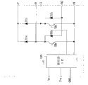
图1是本发明的PFC模块的电路图。
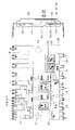
图2是以往的PFC模块的结构图。
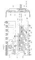
图3是实施方式1的PFC模块的结构图。
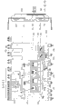
图4是实施方式2的PFC模块的结构图。
图5是实施方式3的PFC模块的结构图。
具体实施方式
实施方式1
图1是本发明的半导体模块即PFC模块的电路图。如该图所示,该PFC模块具有:由第一~第四二极管D1R、D1S、D2R、D2S构成的二极管桥;功率因数改善用的第一以及第二开关元件SWR、SWS;控制该第一以及第二开关元件SWR、SWS的驱动器IC100。
二极管桥如下构成:具有阴极彼此连接的上臂的第一以及第二二极管D1R、D1S及阳极彼此连接的下臂的第三以及第四二极管D2R、D2S,第一二极管D1R和第三二极管D2R串联连接并且第二二极管D1S和第四二极管D2S串联连接。第一二极管D1R的阳极和第三二极管D2R的阴极连接的R端子、以及第二二极管D1S的阳极和第四二极管D2S的阴极连接的S端子是施加交流电源的输入端子。
此外,第一以及第二二极管D1R、D1S的阴极连接的P端子是高电位侧输出端子。第一开关元件SWR连接在第一二极管D1R与第三二极管D2R之间的连接节点(R端子)和作为低电位侧输出端子的N端子之间。第二开关元件SWS连接在第二二极管D1S与第四二极管D2S之间的连接节点(S端子)和N端子之间。
外部的控制IC(未图示)连接到第三以及第四二极管D2R、D2S的阳极连接的N2端子。该控制IC基于N2端子的信号向驱动器IC100的VIN端子供给控制信号,从而控制第一以及第二开关元件SWR、SWS,进行预定的功率因数改善的动作。并且,图1所示的VD端子是驱动器IC100的电源端子,GND端子是接地端子。
此处,作为针对本发明的比较例,对以往的PFC模块的结构进行说明。图2是表示其结构的平面图以及剖面图。在以往的PFC模块中,第一~第四二极管D1R、D1S、D2R、D2S是采用Si形成的肖特基势垒二极管,第一以及第二开关元件SWR、SWS是采用Si形成的例如IGBT。即,第一~第四二极管D1R、D1S、D2R、D2S及第一以及第二开关元件SWR、SWS都是Si器件。
如图2所示,在该PFC模块中,第一以及第二二极管D1R、D1S的芯片搭载在起到P端子的功能的引线框架104(第一引线框架)上。此外,第三二极管D2R以及第一开关元件SWR的芯片搭载在起到R端子的功能的引线框架102(第二引线框架)上。第四二极管D2S以及第二开关元件SWS的芯片搭载在起到S端子的功能的引线框架103(第三引线框架)上。此外,驱动器IC100搭载在起到在其控制中使用的控制端子(VIN端子、VD端子、GND端子等)的功能的预定的引线框架上。
在图2中,引线框架101起到N端子的功能,引线框架105起到N2端子的功能。各芯片和引线框架经由导线布线110进行连接。
以上的各结构要素被构成该PFC模块的壳体200的模塑树脂保持。引线框架101~104的一部分作为外部连接端子从壳体200的一个侧面突出,引线框架105与驱动器IC100的控制端子(VIN端子、VD端子、GND端子等)一起从壳体200的另一个侧面突出。此外,在该PFC模块中设置有贯通壳体200的安装用的贯通孔121、122。
如图2的右侧示出的剖面图所示,在以往的PFC模块中,引线框架101~104在壳体200的内部向下方弯曲,使这些引线框架101~104的芯片搭载部的下表面从壳体200的底面露出。热导率高的绝缘片120贴附在引线框架101~104露出的部分。利用该结构,第一~第四二极管D1R、D1S、D2R、D2S及第一以及第二开关元件SWR的热量容易向外部放出。
以下,对本发明的实施方式1的PFC模块的结构进行说明。在图3中示出其结构。在图3中,对具有与图2示出的要素相同的功能的要素标注相同的附图标记。
在本实施方式中,使作为功率控制用的芯片(功率芯片)的第一~第四二极管D1R、D1S、D2R、D2S及第一以及第二开关元件SWR、SWS中的作为二极管桥的上臂的第一以及第二二极管D1R、D1S为SiC器件的肖特基势垒二极管。其他的功率芯片与现有技术同样,第三以及第四二极管D2R、D2S是Si器件的肖特基势垒二极管、第一以及第二开关元件SWR、SWS是Si器件的IGBT等。
作为二极管桥的上臂的第一以及第二二极管D1R、D1S除了起到整流元件的功能以外,还起到利用第一以及第二开关元件SWR、SWS进行的PFC动作时的回流二极管的功能。特别是,在PFC控制中,第一以及第二开关元件SWR、SWS进行高频率动作,所以,第一以及第二二极管D1R、D1S的回流动作时的恢复损失在很大程度上有助于PFC模块整体的损失。通过使第一以及第二二极管D1R、D1S为低损失且恢复特性优良的SiC器件,能够使PFC模块的损失大幅度减少。此外,不是全部功率芯片而是限于仅将第一以及第二二极管D1R、D1S进行SiC器件化,所以,也能够抑制成本的上升。
此外,如在图3中示出的剖面图所示,搭载第一以及第二二极管D1R、D1S的引线框架104在壳体200的内部不向下方(第一以及第二二极管D1R、D1S搭载面的垂直方向)弯曲。在该情况下,被认为损失了第一以及第二二极管D1R、D1S的散热性,但是,由于SiC器件在耐热性方面优良,所以没有问题。此外,以往损失大的第一以及第二二极管D1R、D1S的损失变小,发热也被抑制,所以,通过省略图2所示的绝缘片120,也能够谋求削减成本。
实施方式2
图4是实施方式2的PFC模块的结构图。在本实施方式中,在壳体200的内部将作为SiC器件的第一以及第二二极管D1R、D1S配设在第三以及第四二极管D2R、D2S和第一以及第二开关元件SWR、SWS的外侧。即,第一以及第二二极管D1R、D1S配设在引线框架101~104突出的壳体200的一个侧面的附近。此外,与实施方式1相同,搭载第一以及第二二极管D1R、D1S的第一引线框架104在壳体200的内部不向下方(第一以及第二二极管D1R、D1S搭载面的垂直方向)弯曲。
根据该结构,能够将连接第一以及第二二极管D1R、D1S和引线框架102、103的导线布线110变短。该导线布线110的长度影响PFC模块的浪涌电流耐受性,若将其变短,则能够提高浪涌电流耐受性。例如,在600V·20A(rms)额定值的PFC模块中,能够使连接第一以及第二二极管D1R、D1S和引线框架102、104的导线布线110的长度为现有技术的一半左右(将现有技术的10mm的长度变为5mm)。
实施方式3
图5是实施方式3的PFC模块的结构图。在本实施方式中,与实施方式2相同,在壳体200的内部,将作为SiC器件的第一以及第二二极管D1R、D1S配设在第三以及第四二极管D2R、D2S和第一以及第二开关元件SWR、SWS的外侧(引线框架101~104突出的壳体200的一个侧面的附近)。
此外,SiC器件为低电阻,所以,能够实现芯片的小型化。例如,在600V·20A(rms)额定值的模块中,能够使第一以及第二二极管D1R、D1S的芯片尺寸变为一半左右。因此,若使第一以及第二二极管D1R、D1S靠近外侧,则在壳体200的中央部形成空间。在本实施方式中,在该空间配设贯通孔122。即,在平面图中,第一以及第二二极管D1R、D1S的至少一方配设在贯通孔122和上述壳体200的一个侧面之间(在图5的平面图中,贯通孔122和第一以及第二二极管D1R、D1S纵向排列)。
根据本实施方式,能够靠近壳体200的内侧配设贯通孔122,所以,能够实现PFC模块的封装尺寸的小型化。例如,在600V·20A(rms)额定值的模块中,能够使封装的长度(壳体200的长度)比实施方式1、2(图3以及图4)短4mm左右。并且,图5的虚线表示实施方式1、2的壳体200的形状以及贯通孔122的位置。
如上所述,本发明有效地利用高耐电压、低损失以及高耐热这样的SiC器件的特性。这些特性不限于SiC器件,还有采用了其他宽带隙半导体的半导体器件。因此,可以使第一以及第二二极管D1R、D1S为采用SiC以外的宽带隙半导体形成的肖特基势垒二极管,能够得到与上述相同的效果。
附图标记说明:
D1R 第一二极管
D1S 第二二极管
D2R 第三二极管
D2S 第四二极管
SWR 第一开关元件
SWS 第二开关元件
100 驱动器IC
101~105 引线框架
110 导线布线
121、122 贯通孔
200 壳体。
Claims (5)
1.一种半导体模块,其特征在于,具有:
二极管桥,具有阴极彼此连接的第一以及第二二极管及阳极彼此连接的第三以及第四二极管,所述第一以及第三二极管串联连接,所述第二以及第四二极管串联连接;
第一开关元件,与所述第一二极管和第三二极管的连接节点连接;以及
第二开关元件,与所述第二二极管和第四二极管的连接节点连接,
所述第一以及第二二极管是采用宽带隙半导体形成的肖特基势垒二极管,
所述第三以及第四二极管及所述第一以及第二开关元件是采用硅形成的肖特基势垒二极管以及开关元件。
2.如权利要求1所述的半导体模块,其特征在于,还具有:
第一引线框架,搭载所述第一以及第二二极管;
第二引线框架,搭载所述第三二极管以及第一开关元件;
第三引线框架,搭载所述第四二极管以及第二开关元件;以及
模塑树脂,保持所述第一~第四二极管、第一以及第二开关元件及所述第一~第三引线框架并且构成该半导体模块的壳体,
所述第一~第三引线框架的一部分作为外部连接端子从由所述模塑树脂构成的所述壳体的一个侧面突出,
在所述壳体的内部,所述第一以及第二二极管与所述第三以及第四二极管及所述第一以及第二开关元件相比,配设在所述一个侧面的附近。
3.如权利要求2所述的半导体模块,其特征在于,
在所述壳体的内部,所述第一引线框架不向所述第一以及第二二极管的搭载面的垂直方向弯曲。
4.如权利要求2或3所述的半导体模块,其特征在于,
在所述壳体上形成有贯通该壳体的贯通孔,
在平面图中,所述第一以及第二二极管的至少一方配设在所述壳体的所述贯通孔和所述一个侧面之间。
5.如权利要求1~3的任意一项所述的半导体模块,其特征在于,
还具有驱动所述第一以及第二开关元件的驱动器IC。
Priority Applications (1)
| Application Number | Priority Date | Filing Date | Title |
|---|---|---|---|
| CN201310265179.9A CN103325759B (zh) | 2011-02-14 | 2011-12-30 | 半导体模块 |
Applications Claiming Priority (2)
| Application Number | Priority Date | Filing Date | Title |
|---|---|---|---|
| JP2011-028184 | 2011-02-14 | ||
| JP2011028184A JP5484372B2 (ja) | 2011-02-14 | 2011-02-14 | 半導体モジュール |
Related Child Applications (1)
| Application Number | Title | Priority Date | Filing Date |
|---|---|---|---|
| CN201310265179.9A Division CN103325759B (zh) | 2011-02-14 | 2011-12-30 | 半导体模块 |
Publications (1)
| Publication Number | Publication Date |
|---|---|
| CN102637679A true CN102637679A (zh) | 2012-08-15 |
Family
ID=46622021
Family Applications (2)
| Application Number | Title | Priority Date | Filing Date |
|---|---|---|---|
| CN201110453505XA Pending CN102637679A (zh) | 2011-02-14 | 2011-12-30 | 半导体模块 |
| CN201310265179.9A Active CN103325759B (zh) | 2011-02-14 | 2011-12-30 | 半导体模块 |
Family Applications After (1)
| Application Number | Title | Priority Date | Filing Date |
|---|---|---|---|
| CN201310265179.9A Active CN103325759B (zh) | 2011-02-14 | 2011-12-30 | 半导体模块 |
Country Status (3)
| Country | Link |
|---|---|
| US (1) | US8643026B2 (zh) |
| JP (1) | JP5484372B2 (zh) |
| CN (2) | CN102637679A (zh) |
Cited By (2)
| Publication number | Priority date | Publication date | Assignee | Title |
|---|---|---|---|---|
| CN104347611A (zh) * | 2013-08-09 | 2015-02-11 | 三菱电机株式会社 | 半导体装置 |
| CN106463420A (zh) * | 2014-05-12 | 2017-02-22 | 三菱电机株式会社 | 电力用半导体装置及其制造方法 |
Families Citing this family (6)
| Publication number | Priority date | Publication date | Assignee | Title |
|---|---|---|---|---|
| JP5875402B2 (ja) * | 2012-02-17 | 2016-03-02 | 三菱電機株式会社 | パワーモジュール及び空調装置 |
| JP2014086536A (ja) * | 2012-10-23 | 2014-05-12 | Renesas Electronics Corp | 半導体装置および半導体装置の製造方法 |
| JP6312170B2 (ja) * | 2014-04-08 | 2018-04-18 | 三菱電機株式会社 | モールドモジュール |
| JP6537246B2 (ja) * | 2014-10-16 | 2019-07-03 | 京セラ株式会社 | パワーモジュール及びパワーユニット |
| US11411120B2 (en) | 2017-09-05 | 2022-08-09 | Ulvac, Inc. | Method for manufacturing semiconductor device using plasma CVD process |
| JP7109347B2 (ja) * | 2018-12-03 | 2022-07-29 | 三菱電機株式会社 | 半導体装置および電力変換装置 |
Citations (2)
| Publication number | Priority date | Publication date | Assignee | Title |
|---|---|---|---|---|
| JP2000138343A (ja) * | 1998-10-30 | 2000-05-16 | Mitsubishi Electric Corp | 半導体装置 |
| WO2009136591A1 (ja) * | 2008-05-08 | 2009-11-12 | トヨタ自動車株式会社 | 半導体装置 |
Family Cites Families (11)
| Publication number | Priority date | Publication date | Assignee | Title |
|---|---|---|---|---|
| SE9502249D0 (sv) | 1995-06-21 | 1995-06-21 | Abb Research Ltd | Converter circuitry having at least one switching device and circuit module |
| JP3201277B2 (ja) | 1996-09-11 | 2001-08-20 | 株式会社日立製作所 | 半導体装置 |
| JPH11233712A (ja) | 1998-02-12 | 1999-08-27 | Hitachi Ltd | 半導体装置及びその製法とそれを使った電気機器 |
| JP4450530B2 (ja) | 2001-07-03 | 2010-04-14 | 三菱電機株式会社 | インバータモジュール |
| JP3676737B2 (ja) * | 2002-01-23 | 2005-07-27 | 三菱電機株式会社 | モータ駆動装置及び送風機及び圧縮機及び冷凍空調装置 |
| JP4262453B2 (ja) * | 2002-07-15 | 2009-05-13 | 三菱電機株式会社 | 電力半導体装置 |
| JP4222193B2 (ja) * | 2003-11-26 | 2009-02-12 | トヨタ自動車株式会社 | 半導体装置 |
| US7355368B2 (en) * | 2004-08-12 | 2008-04-08 | International Rectifier Corporation | Efficient in-rush current limiting circuit with dual gated bidirectional hemts |
| JP2008060430A (ja) * | 2006-08-31 | 2008-03-13 | Daikin Ind Ltd | 電力変換装置 |
| US8076699B2 (en) * | 2008-04-02 | 2011-12-13 | The Hong Kong Univ. Of Science And Technology | Integrated HEMT and lateral field-effect rectifier combinations, methods, and systems |
| KR101740684B1 (ko) * | 2009-10-30 | 2017-05-26 | 가부시키가이샤 한도오따이 에네루기 켄큐쇼 | 파워 다이오드, 정류기 및 그것을 가지는 반도체 장치 |
-
2011
- 2011-02-14 JP JP2011028184A patent/JP5484372B2/ja active Active
- 2011-11-17 US US13/298,711 patent/US8643026B2/en active Active
- 2011-12-30 CN CN201110453505XA patent/CN102637679A/zh active Pending
- 2011-12-30 CN CN201310265179.9A patent/CN103325759B/zh active Active
Patent Citations (3)
| Publication number | Priority date | Publication date | Assignee | Title |
|---|---|---|---|---|
| JP2000138343A (ja) * | 1998-10-30 | 2000-05-16 | Mitsubishi Electric Corp | 半導体装置 |
| JP4073559B2 (ja) * | 1998-10-30 | 2008-04-09 | 三菱電機株式会社 | 半導体装置 |
| WO2009136591A1 (ja) * | 2008-05-08 | 2009-11-12 | トヨタ自動車株式会社 | 半導体装置 |
Cited By (4)
| Publication number | Priority date | Publication date | Assignee | Title |
|---|---|---|---|---|
| CN104347611A (zh) * | 2013-08-09 | 2015-02-11 | 三菱电机株式会社 | 半导体装置 |
| CN104347611B (zh) * | 2013-08-09 | 2017-09-01 | 三菱电机株式会社 | 半导体装置 |
| CN106463420A (zh) * | 2014-05-12 | 2017-02-22 | 三菱电机株式会社 | 电力用半导体装置及其制造方法 |
| CN106463420B (zh) * | 2014-05-12 | 2019-07-26 | 三菱电机株式会社 | 电力用半导体装置及其制造方法 |
Also Published As
| Publication number | Publication date |
|---|---|
| US20120206196A1 (en) | 2012-08-16 |
| US8643026B2 (en) | 2014-02-04 |
| CN103325759A (zh) | 2013-09-25 |
| JP5484372B2 (ja) | 2014-05-07 |
| JP2012169397A (ja) | 2012-09-06 |
| CN103325759B (zh) | 2016-04-13 |
Similar Documents
| Publication | Publication Date | Title |
|---|---|---|
| CN102637679A (zh) | 半导体模块 | |
| CN103782380B (zh) | 半导体模块 | |
| US10104797B2 (en) | Power module, power converter and manufacturing method of power module | |
| US9147622B2 (en) | Power module semiconductor device | |
| US9979314B2 (en) | Power semiconductor module and power conversion device | |
| KR101443972B1 (ko) | 일체형 전력 반도체 모듈 | |
| US11251106B2 (en) | Packaging structure of a SiC MOSFET power module and manufacturing method thereof | |
| KR101321277B1 (ko) | 전력 모듈 패키지 및 그 제조방법 | |
| CN202042483U (zh) | 一种功率半导体器件的封装结构 | |
| JP2012169397A5 (zh) | ||
| JP4872345B2 (ja) | 電力変換装置のインバータモジュール | |
| CN104160502A (zh) | 半导体模块 | |
| JP2002238260A (ja) | 半導体装置 | |
| US10186978B2 (en) | Modular power conversion semiconductor device | |
| US10148190B2 (en) | Power conversion device | |
| JP2019067813A (ja) | 半導体モジュール | |
| US10804189B2 (en) | Power device package structure | |
| CN109427744B (zh) | Ipm模块、车辆及ipm模块的制作方法 | |
| Longford et al. | Utilising advanced packaging technologies to enable smaller, more efficient GaN power devices | |
| CN212209492U (zh) | 功率模块 | |
| US20230197691A1 (en) | Semiconductor power module and power conversion apparatus | |
| CN213242543U (zh) | 一种增加芯片面积的引线框架封装结构 | |
| CN219917162U (zh) | 功率模块 | |
| CN218868437U (zh) | 车载充电机 | |
| CN216928587U (zh) | 半导体模块 |
Legal Events
| Date | Code | Title | Description |
|---|---|---|---|
| C06 | Publication | ||
| PB01 | Publication | ||
| C10 | Entry into substantive examination | ||
| SE01 | Entry into force of request for substantive examination | ||
| C02 | Deemed withdrawal of patent application after publication (patent law 2001) | ||
| WD01 | Invention patent application deemed withdrawn after publication |
Application publication date: 20120815 |