WO2025120939A1 - 銅合金板、電子部品及び銅合金板の製造方法 - Google Patents
銅合金板、電子部品及び銅合金板の製造方法 Download PDFInfo
- Publication number
- WO2025120939A1 WO2025120939A1 PCT/JP2024/031403 JP2024031403W WO2025120939A1 WO 2025120939 A1 WO2025120939 A1 WO 2025120939A1 JP 2024031403 W JP2024031403 W JP 2024031403W WO 2025120939 A1 WO2025120939 A1 WO 2025120939A1
- Authority
- WO
- WIPO (PCT)
- Prior art keywords
- copper alloy
- alloy sheet
- mass
- sheet according
- annealing
- Prior art date
- Legal status (The legal status is an assumption and is not a legal conclusion. Google has not performed a legal analysis and makes no representation as to the accuracy of the status listed.)
- Pending
Links
Images
Classifications
-
- C—CHEMISTRY; METALLURGY
- C22—METALLURGY; FERROUS OR NON-FERROUS ALLOYS; TREATMENT OF ALLOYS OR NON-FERROUS METALS
- C22C—ALLOYS
- C22C9/00—Alloys based on copper
- C22C9/06—Alloys based on copper with nickel or cobalt as the next major constituent
-
- C—CHEMISTRY; METALLURGY
- C22—METALLURGY; FERROUS OR NON-FERROUS ALLOYS; TREATMENT OF ALLOYS OR NON-FERROUS METALS
- C22F—CHANGING THE PHYSICAL STRUCTURE OF NON-FERROUS METALS AND NON-FERROUS ALLOYS
- C22F1/00—Changing the physical structure of non-ferrous metals or alloys by heat treatment or by hot or cold working
-
- C—CHEMISTRY; METALLURGY
- C22—METALLURGY; FERROUS OR NON-FERROUS ALLOYS; TREATMENT OF ALLOYS OR NON-FERROUS METALS
- C22F—CHANGING THE PHYSICAL STRUCTURE OF NON-FERROUS METALS AND NON-FERROUS ALLOYS
- C22F1/00—Changing the physical structure of non-ferrous metals or alloys by heat treatment or by hot or cold working
- C22F1/08—Changing the physical structure of non-ferrous metals or alloys by heat treatment or by hot or cold working of copper or alloys based thereon
-
- H—ELECTRICITY
- H01—ELECTRIC ELEMENTS
- H01B—CABLES; CONDUCTORS; INSULATORS; SELECTION OF MATERIALS FOR THEIR CONDUCTIVE, INSULATING OR DIELECTRIC PROPERTIES
- H01B1/00—Conductors or conductive bodies characterised by the conductive materials; Selection of materials as conductors
- H01B1/02—Conductors or conductive bodies characterised by the conductive materials; Selection of materials as conductors mainly consisting of metals or alloys
- H01B1/026—Alloys based on copper
Definitions
- the present invention relates to copper alloy sheets, electronic components, and methods for manufacturing copper alloy sheets.
- Corson alloys are alloys in which intermetallic compounds such as Ni-Si, Co-Si, and Ni-Co-Si are precipitated in a Cu matrix. Corson alloys are used in electronic components because they have both high strength and high electrical conductivity. For example, they can be used as lead frames that support and fix semiconductor elements in semiconductor packages and form internal wiring (see, for example, Patent Document 1).
- Lead frames are manufactured, for example, by pressing a copper alloy sheet.
- annealing may be performed for a short period of time.
- the hardness of the copper alloy sheet may decrease due to annealing.
- the invention described in Patent Document 1 aims to improve the strength and surface smoothness of the etched surface, but sufficient consideration has not been given to the reduction in hardness that accompanies the reduction in heat resistance after annealing.
- the present invention provides a copper alloy sheet, electronic component, and method for manufacturing the copper alloy sheet that has excellent heat resistance and high hardness even after annealing.
- a copper alloy sheet containing 1.50-4.60 mass% Ni, 0.10-0.80 mass% Co, 0.10-1.30 mass% Si, with the balance being Cu and unavoidable impurities, and having a Vickers hardness of 250 HV or more after annealing the copper alloy sheet at 450°C for 5 minutes.
- an electronic component that includes the above-mentioned copper alloy plate.
- the present invention provides a copper alloy sheet, electronic components, and a method for manufacturing a copper alloy sheet that has excellent heat resistance and high hardness even after annealing.
- the copper alloy sheet according to the present embodiment is a copper alloy sheet containing 1.50 to 4.60 mass% Ni, 0.10 to 0.80 mass% Co, 0.10 to 1.30 mass% Si, and the balance being Cu and unavoidable impurities. That is, the copper alloy sheet according to the present embodiment is a Cu-Ni-Co-Si based alloy sheet.
- Ni, Co, Si Content Ni, Co and Si form precipitated particles of Cu-Ni-Co-Si system intermetallic compounds by carrying out an appropriate heat treatment, and this can improve the electrical conductivity, strength and heat resistance of the copper alloy.
- the Ni concentration is preferably 2.00 mass% or more, more preferably 2.30 mass% or more, even more preferably 3.00 mass% or more, and even more preferably 3.50 mass% or more.
- the Ni concentration is more than 4.60 mass%, the desired electrical conductivity cannot be obtained.
- the Ni concentration is preferably 4.50 mass% or less, more preferably 4.30 mass% or less, even more preferably 4.00 mass% or less, and even more preferably 3.70 mass% or less.
- the Si concentration is preferably 0.30 mass% or more, more preferably 0.50 mass% or more, even more preferably 0.70 mass% or more, and even more preferably 0.80 mass% or more.
- the Si concentration is more than 1.30 mass%, the desired conductivity cannot be obtained.
- the Si concentration is preferably 1.20 mass% or less, more preferably 1.10 mass% or less, even more preferably 1.00 mass% or less, and even more preferably 0.90 mass% or less.
- the Co concentration is set to 0.10 mass% or more.
- the Co concentration is preferably 0.15 to 0.80 mass%, more preferably 0.15 to 0.70 mass%, even more preferably 0.20 to 0.50 mass%, and even more preferably 0.20 to 0.40 mass%.
- the copper alloy sheet according to this embodiment preferably contains Ni and Co in total 1.60 mass% or more, more preferably 2.28 mass% or more, even more preferably 3.00 mass% or more, and even more preferably 3.50 mass% or more.
- the copper alloy sheet according to this embodiment preferably contains Ni and Co in total 4.50 mass% or less, more preferably 4.30 mass% or less, and even more preferably 4.00 mass% or less.
- the ratio of Co to Ni is preferably 0.05 to 0.10, more preferably 0.05 to 0.09, and even more preferably 0.05 to 0.08.
- Ni-Co-Si precipitates formed from Ni, Co, and Si are considered to be intermetallic compounds mainly composed of (Ni+Co)Si.
- the mass ratio of the total of Ni and Co to Si ((Ni+Co)/Si) is preferably 3.4 to 5.4, more preferably 3.8 to 5.0, and even more preferably 4.0 to 4.5.
- At least one element selected from the group consisting of Mg, Fe, P, Cr, Ag, Zn, Sn, Pb, Zr, Al, As, Se, Te, Sb, Bi, Au, Ti, Nb, V, Ta, W, Mo, and Mn improves manufacturability such as improving hot workability by refining the ingot structure by adding a predetermined amount, and also has the effect of improving the strength, electrical conductivity, and heat resistance of the copper alloy sheet. Therefore, by adding one or more of these additive elements according to the required characteristics of the copper alloy sheet according to this embodiment, further improvement in the characteristics of the copper alloy sheet can be expected.
- the copper alloy sheet according to this embodiment preferably further contains 0.01 to 2.00 mass% in total of one or more elements selected from the group consisting of Mg, Fe, P, Cr, Ag, Zn, Sn, Pb, Zr, Al, As, Se, Te, Sb, Bi, Au, Ti, Nb, V, Ta, W, Mo, and Mn.
- the total content of the added elements is preferably 0.03 to 1.00 mass%, and more preferably 0.05 to 0.50 mass%.
- Cr precipitates in the copper matrix alone or as a compound with Si by performing an appropriate heat treatment, and can improve hot rolling properties, and also has the effect of improving the strength, electrical conductivity, and heat resistance of the copper alloy sheet according to this embodiment.
- the Cr content exceeds 0.500 mass%, coarse inclusions that do not contribute to strengthening are formed, and workability may be impaired.
- Cr can be contained in the Cu-Ni-Co-Si alloy in an amount of 0.05 to 0.50 mass%, preferably 0.01 to 0.50 mass%, more preferably 0.20 to 0.50 mass%, and even more preferably 0.20 to 0.30 mass%.
- the copper alloy sheet according to this embodiment can contain 0.005 to 0.50 mass%, preferably 0.01 to 0.50 mass%, more preferably 0.05 to 0.50 mass%, and even more preferably 0.10 to 0.30 mass% of Mg in the Cu-Ni-Co-Si alloy.
- the copper alloy sheet according to this embodiment is made up of Cu and inevitable impurities, the remainder being components other than those mentioned above.
- inevitable impurities refer to impurity elements that are unavoidably mixed into the copper alloy sheet during the manufacturing process.
- concentration of each element of the inevitable impurities can be, for example, less than 0.001% by mass, and is preferably 0% (undetectable).
- the composition of copper alloys can be measured using X-ray fluorescence analysis.
- the X-ray fluorescence analysis device that can be used is a Simultix 14 manufactured by Rigaku Corporation or an equivalent device.
- the analysis surface can be machined or mechanically polished so that the maximum surface roughness Rz (JIS B 0601:2013) is 6.3 ⁇ m or less.
- Rz JIS B 0601:2013
- the metal is cast into a shape of 30-40 mm ⁇ and 50-80 mm thick, then cut into a thickness of 10-20 mm, and the cut surface is used as the analysis surface.
- X-ray fluorescence analysis is performed based on JIS K 0119:2008, and measurements are made using the wavelength dispersion method.
- the composition of the copper alloy can also be measured by wet analysis.
- Ni the copper separation dimethylglyoxime nickel gravimetric method (JIS H1056:2003) can be used, and for Si, the silicon dioxide gravimetric method (JIS H1061:2006) can be used.
- ICP optical emission spectroscopy can be used, and for analysis of other added elements, the internal standard method is used, with Y (yttrium) being used as the internal standard. An element other than Y can be selected as the internal standard.
- ICP optical emission spectroscopy measurements are performed using a Hitachi High-Tech Science ICP optical emission spectroscopy analyzer (ICP-OES) SPS3100 or an equivalent device.
- a sample of the copper alloy is dissolved in a mixed acid containing hydrochloric acid and nitric acid (containing hydrochloric acid, nitric acid, and water in a volume ratio of 2:1:2) and then diluted.
- a mixed acid containing hydrochloric acid and nitric acid containing hydrochloric acid, nitric acid, and water in a volume ratio of 2:1:2
- the shape of the copper alloy plate according to this embodiment is not particularly limited as long as it is a three-dimensional shape having a predetermined thickness.
- the "plate” of the copper alloy plate includes sheets, strips, and foils.
- the copper alloy plate according to this embodiment includes not only copper alloy plates before processing for use in electronic components, but also copper alloy plates during or after processing.
- the thickness of the copper alloy plate is, for example, 0.03 to 1.2 mm.
- the thickness is preferably 0.03 to 0.60 mm, and more preferably 0.08 to 0.30 mm.
- the copper alloy sheet according to the present embodiment has a Vickers hardness of 250 HV or more after annealing the copper alloy sheet at 450 ° C. for 5 minutes.
- residual stress may occur in the copper alloy sheet.
- short-term annealing may be performed, but if the heat resistance of the copper alloy sheet is low due to this annealing, the copper alloy sheet may soften and deformation may occur in the copper alloy sheet after processing.
- the copper alloy sheet according to the present embodiment since it has heat resistance against short-term annealing for reducing residual stress, deformation is unlikely to occur even after short-term annealing is applied after processing the copper alloy sheet, and the target Vickers hardness can be achieved.
- the copper alloy according to this embodiment has a Vickers hardness of 262 HV or more, more preferably 280 HV or more, and more preferably 290 HV or more after the copper alloy sheet is annealed at 450°C for 5 minutes.
- the upper limit of the Vickers hardness after the copper alloy sheet is annealed at 450°C for 5 minutes is not particularly limited, but may be 350 HV or less, 320 HV or less, or 300 HV or less.
- the copper alloy according to this embodiment has a Vickers hardness of 262 to 350 HV, or even 280 to 350 HV, or even 290 to 320 HV after the copper alloy sheet is annealed at 450°C for 5 minutes.
- the Vickers hardness of the copper alloy sheet can be measured in accordance with JIS Z 2244-1:2020 by the method described in the Examples section below.
- the Vickers hardness of the copper alloy sheet after annealing can be controlled to a desired range by controlling the composition of the copper alloy sheet within the above range and manufacturing it by the manufacturing method described below.
- the Vickers hardness can be adjusted to be larger by, for example, increasing the value of X in formula (1) in the manufacturing method described below.
- the copper alloy sheet according to the present embodiment may have a tensile strength of 870 MPa or more in a direction parallel to the rolling direction. By having a tensile strength of 870 MPa or more, it is possible to suppress deformation of the copper alloy sheet when manufacturing electronic components using the copper alloy sheet.
- the copper alloy sheet according to the present embodiment more preferably has a tensile strength of 930 MPa or more in a direction parallel to the rolling direction.
- the upper limit of the tensile strength in the direction parallel to the rolling direction is not particularly limited, but the tensile strength may be, for example, 1200 MPa or less or 1100 MPa or less.
- the copper alloy sheet according to the present embodiment may have a tensile strength of 900 MPa or more in a direction perpendicular to the rolling direction, more preferably 950 MPa or more, and even more preferably 977 MPa or more.
- the tensile strength of the copper alloy sheet can be measured in accordance with JIS Z 2241:2011 by the method described in the Examples section below.
- the copper alloy sheet according to this embodiment may have a 0.2% proof stress of 850 MPa or more in a direction parallel to the rolling direction. This makes it possible to more effectively suppress deformation of the copper alloy sheet during the manufacture of electronic components.
- the 0.2% proof stress in a direction parallel to the rolling direction is preferably 870 MPa or more, more preferably 900 MPa or more, and even more preferably 936 MPa or more.
- the upper limit of the 0.2% proof stress in a direction parallel to the rolling direction is not particularly limited, but the 0.2% proof stress may be, for example, 1200 MPa or less, 1100 MPa or less, or 1000 MPa or less.
- the 0.2% proof stress can be measured in accordance with JIS Z 2241:2011 by the method described in the Examples section below.
- the copper alloy sheet according to the present embodiment may have a conductivity of 35.0% IACS or more.
- the conductivity of 35.0% IACS or more can be effectively used as a copper alloy part of an electronic component.
- the conductivity is preferably 37.0% IACS or more, more preferably 40.0% IACS or more, and even more preferably 40.2% IACS or more.
- the upper limit of the conductivity is not particularly limited, but may be, for example, 90.0% IACS or less, or 80.0% IACS or less.
- Conductivity can be measured by the four-terminal method in accordance with JIS H 0505:1975. A double bridge is used for the measurement, and resistance can be measured based on the average cross-sectional area method. Conductivity can be measured at room temperature (25°C) in the direction parallel to the rolling direction. The gauge length (distance between electrical resistance measurements) can be measured at 50 mm.
- the method for producing a copper alloy sheet according to the present embodiment focuses on the heat resistance of the copper alloy sheet after forming, and adjusts the manufacturing conditions so that the value of X in formula (1) is 5
- the method for manufacturing the copper alloy sheet according to this embodiment can be manufactured by the following method.
- a process is performed in which the raw material of the copper alloy having the desired composition described above is melted and cast.
- the raw material of the copper alloy is melted in the same manner as in the general copper alloy melting method, and then an ingot is manufactured by continuous casting or semi-continuous casting. That is, an atmospheric melting furnace is used to melt raw materials such as electrolytic copper, Ni, Co, and Si to obtain a molten metal with the desired composition. This molten metal is then poured into a mold of the desired dimensions to cast an ingot. After that, homogenization annealing is performed at 800 to 1000°C, and further hot rolling is performed.
- Hot rolling is performed, for example, in several passes at 500 to 900°C.
- the total reduction rate of hot rolling is preferably 90% or more.
- silicides such as Ni-Si compounds, Co-Si compounds, and Cr-Si compounds are dissolved in the Cu matrix, and heat treatment is performed to simultaneously recrystallize the Cu matrix.
- the manufacturing method of the copper alloy sheet according to this embodiment by adjusting the value of X in formula (1) of the copper alloy intermediate after the solution treatment to 582 or more, it is possible to obtain a copper alloy sheet and electronic parts that have excellent heat resistance and a high hardness of 250 HV or more even after annealing.
- the value of X represented by formula (1) is preferably 3000 or more, more preferably 5000 or more, and even more preferably 8000 or more.
- the upper limit of X is not particularly limited, but is typically preferably 17000 or less, more preferably 15000 or less, and even more preferably 13000 or less.
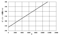
- Figure 1 is a graph showing the relationship between X in the above formula (1) and the Vickers hardness (HV) of the copper alloy sheet after stress relief annealing described later and annealing at 450°C for 5 minutes.
- the tensile strength (A), 0.2% yield strength (B), and electrical conductivity (C) are all values obtained by measuring in a direction parallel to the rolling direction.
- the value of X in the solution treatment process is adjusted by adjusting the heating temperature, material temperature, heating time, etc. during the solution treatment.
- the heating temperature of the solution treatment can be appropriately selected from the range of, for example, 800 to 1100°C.
- the heating temperature of the solution treatment may be 900 to 1100°C or 950 to 1100°C.
- the material temperature can be appropriately selected from the range of, for example, 750 to 950°C.
- the material temperature is slowly cooled to 400 to 500°C.
- the heating time can be appropriately selected from the range of 1 second to 10 minutes.
- the heating temperature of the aging treatment for the copper alloy intermediate after the solution treatment may be, for example, 375 to 625°C, 400 to 550°C, or 450 to 500°C.
- the heating time of the aging treatment may be 1 to 50 hours, 1.5 to 25 hours, or 10 to 15 hours.
- the finish cold rolling after aging treatment may be performed in several passes.
- the total processing degree of the finish cold rolling may be 40% or more. This allows processing strain to be imparted to the copper alloy intermediate, improving its strength. By setting the total processing degree of the finish cold rolling to 40% or more, it is possible to improve the strength in various directions relative to the rolling direction.
- the processing degree of the finish cold rolling is preferably 55% or more, and more preferably 60% or more.
- the processing degree of the finish cold rolling may be 90% or less. This prevents a decrease in electrical conductivity due to processing strain caused by a high processing degree.
- a step of performing stress relief annealing may be included.
- the heating temperature for stress relief annealing may be, for example, 300 to 600°C, preferably 400 to 600°C, and more preferably 420 to 550°C.
- the heating time for stress relief annealing may be, for example, 5 to 900 seconds, or 200 to 650 seconds.
- Strain relief annealing may be performed in air or in an inert atmosphere such as nitrogen or argon gas.
- the copper alloy sheet after stress relief annealing may be cooled by air cooling.
- cold rolling may be performed before the solution treatment, or cold rolling may be performed after the solution treatment and before the aging treatment, and further, the solution treatment and the aging treatment may each be performed two or more times.
- grinding, pickling, polishing, degreasing, facing, shot blasting, trimming, etc. may be appropriately performed as necessary to remove oxide scale from the surface.
- the manufacturing method of the copper alloy sheet according to this embodiment may include a step of annealing the copper alloy sheet after the stress relief annealing step at 300°C or higher for 1 second or more.
- this annealing step after subjecting the copper alloy sheet after the stress relief annealing step to processing such as pressing, the residual stress of the copper alloy sheet caused by processing can be reduced.
- the processed copper alloy sheet that has been subjected to such processing is less likely to deform and has both high electrical conductivity and strength.
- the heating temperature in this annealing process may be 300 to 600°C, or 400 to 500°C.
- the heating time may be 1 second to 60 minutes, 30 seconds to 20 minutes, or 1 minute to 10 minutes.
- the electronic component of the present embodiment is an electronic component comprising the copper alloy plate according to the present embodiment. More specifically, the electronic component according to the present embodiment comprises a copper alloy part manufactured from the above-mentioned copper alloy plate.
- An example of the electronic component is a semiconductor package.
- the fine copper alloy part that can be manufactured from the copper alloy plate according to the present embodiment has improved hardness after processing in the manufacturing process of the electronic component, so that it is preferable to use the copper alloy plate according to the present embodiment for manufacturing a semiconductor package having many fine structures.
- the semiconductor package can be manufactured, for example but not limited to, by manufacturing a lead frame using the copper alloy plate according to this embodiment, then supporting and fixing a semiconductor element on the lead frame, wire bonding the semiconductor element and the leads to form internal wiring, and then sealing the semiconductor element with a specified resin material.
- the electronic component of this embodiment may include the copper alloy plate of the above-mentioned embodiment.
- the copper alloy sheet, electronic component, and method for manufacturing the copper alloy sheet of the present disclosure are not limited to the above examples and can be modified as appropriate.
- a first aspect of the present disclosure is a copper alloy sheet containing 1.50 to 4.60 mass% Ni, 0.10 to 0.80 mass% Co, 0.10 to 1.30 mass% Si, with the balance being Cu and unavoidable impurities, and having a Vickers hardness of 250 HV or more after annealing the copper alloy sheet at 450 ° C. for 5 minutes.
- the second aspect of the present disclosure is the copper alloy sheet according to the first aspect, further containing 0.01 to 2.00 mass% in total of one or more elements selected from the group consisting of Mg, Fe, P, Cr, Ag, Zn, Sn, Pb, Zr, Al, As, Se, Te, Sb, Bi, Au, Ti, Nb, V, Ta, W, Mo, and Mn.
- the third aspect of the present disclosure is the copper alloy sheet according to the first or second aspect, further containing 0.01 to 0.50 mass% Cr.
- the fourth aspect of the present disclosure is a copper alloy sheet according to any one of the first to third aspects, containing 0.20 to 0.50 mass % Co.
- the fifth aspect of the present disclosure is a copper alloy sheet according to any one of the first to fourth aspects, containing Ni and Co in a total amount of 1.60 mass% or more.
- the sixth aspect of the present disclosure is a copper alloy sheet according to any one of the first to fifth aspects, containing Ni and Co in a total amount of 2.28 mass% or more.
- the seventh aspect of the present disclosure is a copper alloy sheet according to any one of the first to sixth aspects, containing Ni and Co in a total amount of 4.50 mass% or less.
- the eighth aspect of the present disclosure is a copper alloy sheet according to any one of the first to seventh aspects, having a Vickers hardness of 262 HV or more.
- the ninth aspect of the present disclosure is a copper alloy sheet according to any one of the first to eighth aspects, which has a Vickers hardness of 350 HV or less.
- the tenth aspect of the present disclosure is a copper alloy sheet according to any one of the first to ninth aspects, in which the tensile strength in the direction parallel to the rolling direction is 870 MPa or more.
- the eleventh aspect of the present disclosure is a copper alloy sheet according to any one of the first to tenth aspects, in which the tensile strength in the direction parallel to the rolling direction is 930 MPa or more.
- the twelfth aspect of the present disclosure is a copper alloy sheet according to any one of the first to eleventh aspects, which has a conductivity of 35.0% IACS or more.
- the thirteenth aspect of the present disclosure is a copper alloy sheet according to any one of the first to twelfth aspects, in which the electrical conductivity is 40.2% IACS or more.
- the fourteenth aspect of the present disclosure is an electronic component comprising a copper alloy sheet according to any one of the first to thirteenth aspects.
- the sixteenth aspect of the present disclosure is a method for producing a copper alloy sheet according to the fifteenth aspect, which includes a step of annealing the copper alloy sheet after the stress relief annealing step at 300°C or higher for one second or more.
- the copper alloys according to the examples and comparative examples having the compositions shown in Table 1 were melted and cast using an air melting furnace.
- the obtained ingots were subjected to homogenization annealing at 980°C for 25 minutes.
- the ingots were hot rolled until the plate thickness reached 10 mm, and then faced.
- solution treatment and aging treatment were performed in this order under the conditions shown in Table 1.
- the obtained intermediate bodies were pickled and polished, and finished cold rolling treatment was performed until the plate thickness reached 0.151 mm with the processing degree shown in Table 1.
- stress relief annealing treatment was performed in the atmosphere under the conditions shown in Table 1.
- the copper alloy plates after stress relief annealing treatment were air-cooled to obtain the copper alloy plates of Example 1 and Comparative Example 1.
- composition The composition of the obtained copper alloy was confirmed by X-ray fluorescence analysis. Simultix 14 manufactured by Rigaku Corporation was used as the X-ray fluorescence analyzer. The copper alloy sheets of Example 1 and Comparative Example 1 were cut or mechanically polished so that the maximum surface roughness Rz (JIS B 0601: 2013) was 6.3 ⁇ m or less. The X-ray fluorescence analysis was performed based on JIS K 0119: 2008 and measured by a wavelength dispersion method.
- the tensile strength in the direction parallel to the rolling direction was measured using a tensile tester (Autocom AC-100KN-C, manufactured by TSE Co., Ltd.) in accordance with JIS Z 2241:2011. Specifically, a JIS Z 2241 No. 13B test piece was prepared from each sample using a press machine so that the tensile direction was parallel to the rolling direction. The conditions for the tensile test were a test piece width of 12.5 mm, a measurement temperature of room temperature (15 to 35°C), a tensile speed (crosshead displacement speed) of 5 mm/min, and a gauge length (gauge length) of 50 mm. The measurement was performed using two test pieces, and the average value of the two data was calculated.
- test pieces were prepared in the same manner as in the above-mentioned tensile strength test, and tests were performed under the same conditions as in the above-mentioned tensile strength test.
- the electrical conductivity was measured by a four-terminal method in accordance with JIS H 0505:1975. A double bridge was used for the measurement, and the resistance was measured based on the average cross-sectional area method. The electrical conductivity was measured at room temperature (25°C) in a direction parallel to the rolling direction. The gage length (distance between electrical resistance measurements) was 50 mm.
- Example 1 (Hardness after annealing)
- Comparative Example 1 (Hardness after annealing)
- the copper alloy sheets of Example 1 and Comparative Example 1 were annealed at 450 ° C. in a nitrogen atmosphere in a tubular furnace for 5 minutes.
- the copper alloy sheets after annealing were cooled to room temperature by air cooling.
- the Vickers hardness of the copper alloy sheets after cooling was measured using a Vickers hardness tester.
- HM-103 manufactured by Mitutoyo Corporation was used.
- the copper alloy sheets cut to 20 mm x 20 mm were filled with resin, mechanically polished, and the central part of the sheet thickness of the rolled parallel cross section of the sample was measured.
- the resin used was an epoxy resin (Epicoat #828) manufactured by Mitsubishi Chemical Corporation, and the hardener used was a hardener (Acmex H-89) manufactured by Nippon Gosei Kako Co., Ltd., which were heated at 100 ° C. for 60 minutes to harden.
- the test force was 490.3 mN
- the indenter approach speed was 60 ⁇ m/s
- the holding time was 15 seconds.
- the average value of the values measured at three points was calculated.
- a 50x objective lens was used for the measurement, and the indentations were spaced apart by 3d or more from the average diagonal length d of the indentations.
- Example 1 compared to Comparative Example 1, a copper alloy material having an excellent balance of strength, electrical conductivity, and heat resistance, and having hardness after annealing suitable for electronic component applications, is obtained.
- a copper alloy sheet having excellent heat resistance and high strength even after annealing and an electronic component including the same can be provided, which may contribute to improving the stability of operation of electronic devices and improving their reliability. Therefore, an embodiment of the present disclosure may contribute to Goal 9 of the United Nations-led Sustainable Development Goals (SDGs), "Build resilient infrastructure, promote inclusive and sustainable industrialization, and foster innovation.”
- SDGs United Nations-led Sustainable Development Goals
Landscapes
- Chemical & Material Sciences (AREA)
- Engineering & Computer Science (AREA)
- Materials Engineering (AREA)
- Mechanical Engineering (AREA)
- Metallurgy (AREA)
- Organic Chemistry (AREA)
- Physics & Mathematics (AREA)
- Thermal Sciences (AREA)
- Crystallography & Structural Chemistry (AREA)
- Conductive Materials (AREA)
Priority Applications (4)
| Application Number | Priority Date | Filing Date | Title |
|---|---|---|---|
| JP2025561694A JPWO2025120939A1 (cg-RX-API-DMAC7.html) | 2023-12-07 | 2024-08-30 | |
| KR1020267013627A KR20260066195A (ko) | 2023-12-07 | 2024-08-30 | 구리 합금판, 전자 부품 및 구리 합금판의 제조 방법 |
| CN202480075136.0A CN122270575A (zh) | 2023-12-07 | 2024-08-30 | 铜合金板、电子部件及铜合金板的制造方法 |
| TW113137556A TW202536205A (zh) | 2023-12-07 | 2024-10-01 | 銅合金板、電子零件及銅合金板之製造方法 |
Applications Claiming Priority (6)
| Application Number | Priority Date | Filing Date | Title |
|---|---|---|---|
| JP2023-207176 | 2023-12-07 | ||
| JP2023207165A JP7648724B1 (ja) | 2023-12-07 | 2023-12-07 | 銅合金及び電子部品 |
| JP2023207176 | 2023-12-07 | ||
| JP2023207186 | 2023-12-07 | ||
| JP2023-207186 | 2023-12-07 | ||
| JP2023-207165 | 2023-12-07 |
Publications (1)
| Publication Number | Publication Date |
|---|---|
| WO2025120939A1 true WO2025120939A1 (ja) | 2025-06-12 |
Family
ID=95980805
Family Applications (1)
| Application Number | Title | Priority Date | Filing Date |
|---|---|---|---|
| PCT/JP2024/031403 Pending WO2025120939A1 (ja) | 2023-12-07 | 2024-08-30 | 銅合金板、電子部品及び銅合金板の製造方法 |
Country Status (5)
| Country | Link |
|---|---|
| JP (1) | JPWO2025120939A1 (cg-RX-API-DMAC7.html) |
| KR (1) | KR20260066195A (cg-RX-API-DMAC7.html) |
| CN (1) | CN122270575A (cg-RX-API-DMAC7.html) |
| TW (1) | TW202536205A (cg-RX-API-DMAC7.html) |
| WO (1) | WO2025120939A1 (cg-RX-API-DMAC7.html) |
Citations (7)
| Publication number | Priority date | Publication date | Assignee | Title |
|---|---|---|---|---|
| JP2006089763A (ja) * | 2004-09-21 | 2006-04-06 | Dowa Mining Co Ltd | 銅合金およびその製造法 |
| JP2006169548A (ja) * | 2004-12-13 | 2006-06-29 | Dowa Mining Co Ltd | 銅合金材料およびその製造法 |
| JP2007100145A (ja) * | 2005-09-30 | 2007-04-19 | Dowa Holdings Co Ltd | 曲げ加工性と疲労特性を改善した銅合金板材 |
| WO2009099198A1 (ja) * | 2008-02-08 | 2009-08-13 | The Furukawa Electric Co., Ltd. | 電気電子部品用銅合金材料 |
| JP2011231393A (ja) * | 2010-04-05 | 2011-11-17 | Dowa Metaltech Kk | 銅合金板材および銅合金板材の製造方法、電気・電子部品 |
| JP2016050326A (ja) * | 2014-08-29 | 2016-04-11 | 三菱マテリアル株式会社 | 電子・電気機器用銅合金、電子・電気機器用銅合金薄板、電子・電気機器用部品及び端子 |
| JP2018070938A (ja) * | 2016-10-27 | 2018-05-10 | Dowaメタルテック株式会社 | 銅合金板材およびその製造方法 |
-
2024
- 2024-08-30 JP JP2025561694A patent/JPWO2025120939A1/ja active Pending
- 2024-08-30 KR KR1020267013627A patent/KR20260066195A/ko active Pending
- 2024-08-30 CN CN202480075136.0A patent/CN122270575A/zh active Pending
- 2024-08-30 WO PCT/JP2024/031403 patent/WO2025120939A1/ja active Pending
- 2024-10-01 TW TW113137556A patent/TW202536205A/zh unknown
Patent Citations (7)
| Publication number | Priority date | Publication date | Assignee | Title |
|---|---|---|---|---|
| JP2006089763A (ja) * | 2004-09-21 | 2006-04-06 | Dowa Mining Co Ltd | 銅合金およびその製造法 |
| JP2006169548A (ja) * | 2004-12-13 | 2006-06-29 | Dowa Mining Co Ltd | 銅合金材料およびその製造法 |
| JP2007100145A (ja) * | 2005-09-30 | 2007-04-19 | Dowa Holdings Co Ltd | 曲げ加工性と疲労特性を改善した銅合金板材 |
| WO2009099198A1 (ja) * | 2008-02-08 | 2009-08-13 | The Furukawa Electric Co., Ltd. | 電気電子部品用銅合金材料 |
| JP2011231393A (ja) * | 2010-04-05 | 2011-11-17 | Dowa Metaltech Kk | 銅合金板材および銅合金板材の製造方法、電気・電子部品 |
| JP2016050326A (ja) * | 2014-08-29 | 2016-04-11 | 三菱マテリアル株式会社 | 電子・電気機器用銅合金、電子・電気機器用銅合金薄板、電子・電気機器用部品及び端子 |
| JP2018070938A (ja) * | 2016-10-27 | 2018-05-10 | Dowaメタルテック株式会社 | 銅合金板材およびその製造方法 |
Also Published As
| Publication number | Publication date |
|---|---|
| TW202536205A (zh) | 2025-09-16 |
| KR20260066195A (ko) | 2026-05-12 |
| CN122270575A (zh) | 2026-06-23 |
| JPWO2025120939A1 (cg-RX-API-DMAC7.html) | 2025-06-12 |
Similar Documents
| Publication | Publication Date | Title |
|---|---|---|
| JP4247922B2 (ja) | 電気・電子機器用銅合金板材およびその製造方法 | |
| CN108431257B (zh) | 电子电气设备用铜合金、电子电气设备用铜合金板条材、电子电气设备用组件、端子、汇流条及继电器用可动片 | |
| WO2011125554A1 (ja) | 電子材料用Cu-Ni-Si-Co系銅合金及びその製造方法 | |
| JP5451674B2 (ja) | 電子材料用Cu−Si−Co系銅合金及びその製造方法 | |
| JP5871443B1 (ja) | 銅合金板材およびその製造方法 | |
| JP4834781B1 (ja) | 電子材料用Cu−Co−Si系合金 | |
| CN103403202A (zh) | Cu-Ni-Si系合金及其制造方法 | |
| WO2014196563A1 (ja) | 銅合金の製造方法および銅合金 | |
| JP7430502B2 (ja) | 銅合金線材及び電子機器部品 | |
| JP5135496B2 (ja) | Cu−Be系銅合金板材およびその製造法 | |
| CN107208191A (zh) | 铜合金材料及其制造方法 | |
| JP5135914B2 (ja) | 電気・電子部品用高強度銅合金の製造方法 | |
| JP6837542B2 (ja) | 耐熱性及び放熱性に優れた銅合金板材 | |
| WO2006093233A1 (ja) | 銅合金とその製造方法 | |
| JP4887851B2 (ja) | Ni−Sn−P系銅合金 | |
| JP2012229467A (ja) | 電子材料用Cu−Ni−Si系銅合金 | |
| JP7648724B1 (ja) | 銅合金及び電子部品 | |
| TW202536205A (zh) | 銅合金板、電子零件及銅合金板之製造方法 | |
| US20070131321A1 (en) | Copper alloy for electric and electronic instruments | |
| WO2025120905A1 (ja) | 銅合金板、電子部品及び銅合金板の製造方法 | |
| WO2025120908A1 (ja) | 銅合金板、電子部品及び銅合金板の製造方法 | |
| WO2025120906A1 (ja) | 銅合金板、電子部品及び銅合金板の製造方法 | |
| KR20260056293A (ko) | 구리 합금판, 전자 부품 및 구리 합금판의 제조 방법 | |
| JP2015224356A (ja) | 銅合金板材およびその製造方法 | |
| WO2026048037A1 (ja) | 銅合金板、電子部品及び銅合金板の製造方法 |
Legal Events
| Date | Code | Title | Description |
|---|---|---|---|
| 121 | Ep: the epo has been informed by wipo that ep was designated in this application |
Ref document number: 24900236 Country of ref document: EP Kind code of ref document: A1 |
|
| ENP | Entry into the national phase |
Ref document number: 2025561694 Country of ref document: JP Kind code of ref document: A |
|
| WWE | Wipo information: entry into national phase |
Ref document number: 2025561694 Country of ref document: JP |
|
| ENP | Entry into the national phase |
Ref document number: 1020267013627 Country of ref document: KR Free format text: ST27 STATUS EVENT CODE: A-0-1-A10-A15-NAP-PA0105 (AS PROVIDED BY THE NATIONAL OFFICE) |
|
| NENP | Non-entry into the national phase |
Ref country code: DE |