WO2025041384A1 - セラミック基板及び電子部品 - Google Patents
セラミック基板及び電子部品 Download PDFInfo
- Publication number
- WO2025041384A1 WO2025041384A1 PCT/JP2024/017566 JP2024017566W WO2025041384A1 WO 2025041384 A1 WO2025041384 A1 WO 2025041384A1 JP 2024017566 W JP2024017566 W JP 2024017566W WO 2025041384 A1 WO2025041384 A1 WO 2025041384A1
- Authority
- WO
- WIPO (PCT)
- Prior art keywords
- electrode
- insulating layer
- element body
- content
- weight
- Prior art date
- Legal status (The legal status is an assumption and is not a legal conclusion. Google has not performed a legal analysis and makes no representation as to the accuracy of the status listed.)
- Pending
Links
Images


Classifications
-
- H—ELECTRICITY
- H05—ELECTRIC TECHNIQUES NOT OTHERWISE PROVIDED FOR
- H05K—PRINTED CIRCUITS; CASINGS OR CONSTRUCTIONAL DETAILS OF ELECTRIC APPARATUS; MANUFACTURE OF ASSEMBLAGES OF ELECTRICAL COMPONENTS
- H05K1/00—Printed circuits
- H05K1/02—Details
- H05K1/03—Use of materials for the substrate
- H05K1/0306—Inorganic insulating substrates, e.g. ceramic, glass
-
- H—ELECTRICITY
- H05—ELECTRIC TECHNIQUES NOT OTHERWISE PROVIDED FOR
- H05K—PRINTED CIRCUITS; CASINGS OR CONSTRUCTIONAL DETAILS OF ELECTRIC APPARATUS; MANUFACTURE OF ASSEMBLAGES OF ELECTRICAL COMPONENTS
- H05K1/00—Printed circuits
- H05K1/16—Printed circuits incorporating printed electric components, e.g. printed resistors, capacitors or inductors
- H05K1/162—Printed circuits incorporating printed electric components, e.g. printed resistors, capacitors or inductors incorporating printed capacitors
-
- H—ELECTRICITY
- H05—ELECTRIC TECHNIQUES NOT OTHERWISE PROVIDED FOR
- H05K—PRINTED CIRCUITS; CASINGS OR CONSTRUCTIONAL DETAILS OF ELECTRIC APPARATUS; MANUFACTURE OF ASSEMBLAGES OF ELECTRICAL COMPONENTS
- H05K1/00—Printed circuits
- H05K1/02—Details
- H05K1/09—Use of materials for the conductive, e.g. metallic pattern
-
- H—ELECTRICITY
- H05—ELECTRIC TECHNIQUES NOT OTHERWISE PROVIDED FOR
- H05K—PRINTED CIRCUITS; CASINGS OR CONSTRUCTIONAL DETAILS OF ELECTRIC APPARATUS; MANUFACTURE OF ASSEMBLAGES OF ELECTRICAL COMPONENTS
- H05K1/00—Printed circuits
- H05K1/16—Printed circuits incorporating printed electric components, e.g. printed resistors, capacitors or inductors
- H05K1/165—Printed circuits incorporating printed electric components, e.g. printed resistors, capacitors or inductors incorporating printed inductors
-
- H—ELECTRICITY
- H05—ELECTRIC TECHNIQUES NOT OTHERWISE PROVIDED FOR
- H05K—PRINTED CIRCUITS; CASINGS OR CONSTRUCTIONAL DETAILS OF ELECTRIC APPARATUS; MANUFACTURE OF ASSEMBLAGES OF ELECTRICAL COMPONENTS
- H05K3/00—Apparatus or processes for manufacturing printed circuits
- H05K3/46—Manufacturing multilayer circuits
- H05K3/4611—Manufacturing multilayer circuits by laminating two or more circuit boards
- H05K3/4626—Manufacturing multilayer circuits by laminating two or more circuit boards characterised by the insulating layers or materials
- H05K3/4629—Manufacturing multilayer circuits by laminating two or more circuit boards characterised by the insulating layers or materials laminating inorganic sheets comprising printed circuits, e.g. green ceramic sheets
Definitions
- the present invention relates to ceramic substrates and electronic components.
- Patent Document 1 discloses a ceramic laminate substrate having a plurality of ceramic layers and an electrode pattern, the ceramic laminate substrate having a terminal electrode and an insulating layer on the outer surface thereof, the terminal electrode having a base layer and an upper layer formed by an electrode pattern, at least a portion of the outer edge of the base layer and the ceramic layer being covered with the insulating layer, and at least a portion of the insulating layer being covered with the upper layer, thereby sandwiching the insulating layer between the upper layer and the base layer.
- the base layer and upper layer of the terminal electrode are in close contact with the insulating layer.
- stress is likely to concentrate on the outer periphery of the terminal electrode. This may result in cracks occurring in the insulating layer directly below the outer periphery of the upper layer. If a crack occurs in the insulating layer from the end of the upper layer, the base layer will stop the crack from progressing. However, because the base layer is thin directly below the insulating layer, the progression of the crack may not be sufficiently stopped, and the crack may progress to the electrodes provided inside the laminated substrate, causing the continuity of the electrodes of the laminated substrate to be interrupted.
- the present invention has been made to solve the above problems, and aims to provide a ceramic substrate that can ensure electrical continuity from the terminal electrodes to the internal conductors. Furthermore, the present invention aims to provide an electronic component that includes the above ceramic substrate.
- FIG. 11 is a cross-sectional view that typically shows a process of forming a second conductive paste layer that becomes a second electrode after firing.
- FIG. 12 is a plan view that typically illustrates a process of forming a second conductive paste layer that becomes a second electrode after firing.
- FIG. 13 is a cross-sectional view illustrating a first modified example of the ceramic substrate.
- FIG. 14 is a cross-sectional view illustrating a second modified example of the ceramic substrate.
- FIG. 15 is a plan view diagrammatically illustrating a second modified example of the ceramic substrate.
- FIG. 16 is a cross-sectional view illustrating a schematic diagram of a third modified example of the ceramic substrate.
- FIG. 17 is a plan view diagrammatically illustrating a third modified example of the ceramic substrate.
- FIG. 18 is a perspective view illustrating an example of an electronic component according to the present invention.
- FIG. 19 is a perspective view showing an input/output terminal and a ground terminal in an example of an electronic component according to the present invention.
- FIG. 20 is an exploded perspective view showing a schematic example of an electronic component according to the present invention.
- the present invention is not limited to the following configurations, and can be modified and applied as appropriate within the scope of the present invention. Note that the present invention also includes a combination of two or more of the individual desirable configurations described below.
- FIG. 1 is a cross-sectional view showing a schematic example of a ceramic substrate of the present invention.
- the ceramic substrate 1 comprises an element body 10 including a ceramic layer, at least one internal conductor 40 provided inside the element body 10, a terminal electrode 20 provided on the outer surface of the element body 10, and an insulating layer 30 provided on the outer surface of the element body 10.
- the base body 10 includes a ceramic layer.
- the base body 10 may be a multilayer ceramic substrate including multiple ceramic layers.
- the material of the element 10 is not particularly limited, but for example, a low temperature co-fired ceramic (LTCC) material may be used.
- the low-temperature sintering ceramic material is a ceramic material that can be sintered at a temperature of 1000° C. or less and can be co-fired with Au, Ag, Cu, etc., which have low resistivity.
- the low-temperature sintering ceramic material include glass composite low-temperature sintering ceramic materials obtained by mixing borosilicate glass with ceramic powder such as alumina, zirconia, magnesia, spinel, forsterite, etc., crystallized glass low-temperature sintering ceramic materials using ZnO-MgO-Al 2 O 3 -SiO 2 crystallized glass, and non-glass low-temperature sintering ceramic materials using BaO-Al 2 O 3 -SiO 2 ceramic powder or Al 2 O 3 -CaO-SiO 2 -MgO-B 2 O 3 ceramic powder.
- the element body 10 may contain glass.
- the element body 10 may be a sintered body of glass ceramics.
- the type of glass is not particularly limited, but examples include borosilicate glass and crystallized glass.
- Examples of materials for the element 10 include: (1) a first ceramic made of at least one of MgAl 2 O 4 and Mg 2 SiO 4 ; (2) a second ceramic made of BaO, RE 2 O 3 (RE is a rare earth element) and TiO 2 ; and (3) a ceramic made of 44.0 to 69.0 wt % RO (R is at least one alkaline earth metal selected from Ba, Ca and Sr), 14.2 to 30.0 wt % SiO 2 , 10.0 to 20.0 wt % B 2 O 3 , 0.5 to 4.0 wt % Al 2 O 3 , and Li 2 and (4) MnO, the glass ceramic composition including the first ceramic at 47.55 to 69.32 wt%, the glass at 6 to 20 wt%, the MnO at 7.5 to 18.5 wt%, and the second ceramic at 0.38 to 1.43 wt%, BaO at 1.33 to 9.5 wt%, and TiO at 0.95 to 6.75 wt%, respectively.
- the glass-ceramic composition may contain up to 0.23 wt. % CuO.
- the glass ceramic composition may contain 3 to 20 wt % of a third ceramic consisting of at least one of Mg 2 Al 4 Si 5 O 18 and BaAl 2 Si 2 O 8 , and may further contain 0.3 wt % or less of CuO in addition to the third ceramic.
- the material for the element body 10 is a glass ceramic including a glass containing Si, B, Al, and Zn, and an aggregate, the glass being 45% by weight or more and 80% by weight or less, and the aggregate being glass ceramic including 20% by weight or more and 50% by weight or less of SiO2 , 20% by weight or less of Al2O3 , and 10% by weight or less of ZnO, relative to the weight of the glass ceramic.
- the above glass-ceramics may contain SiO2 , ZnAl2O4 , and Al2O3 as crystalline phases.
- the glass may have a SiO2 content of 15% by weight or more and 65% by weight or less, a B2O3 content of 11% by weight or more and 30% by weight or less , a weight ratio of SiO2 to B2O3 ( SiO2 / B2O3 ) of 1.21 or more, and a weight ratio of Al2O3 to ZnO ( Al2O3 /ZnO) of 0.75 or more and 1.64 or less.
- the glass in the glass ceramic may be a crystallized glass and may contain ZnAl 2 O 4 as a crystalline phase precipitated from the glass.
- the glass may contain Li 2 O as a minor component, and the Li 2 O content in the glass may be 1.0 wt % or less.
- the crystallization temperature of the glass may be 1000° C. or lower.
- the glass ceramic may have a relative dielectric constant of 5 or less.
- the above glass ceramics may specify the contents of Si, B, Al, and Zn without distinguishing between glass and aggregate.
- Examples of materials in which the contents of Si, B, Al, and Zn are specified without distinguishing between glass and aggregate include glass ceramics containing Si, B, Al, and Zn, in which the SiO 2 content is 52.00% by weight or more and 71.58% by weight or less, the B 2 O 3 content is 6.30% by weight or more and 21.00% by weight or less, the Al 2 O 3 content is 7.63% by weight or more and 22.00% by weight or less, the ZnO content is 5.04% by weight or more and 17.00% by weight or less, and the Li 2 O content is 0.55% by weight or less.
- Table 1 shows examples of the ratios of each element in some glass ceramics.
- the glass ceramic preferably contains 60% by weight or more of SiO2 , 15% by weight or less of B2O3 , 15% by weight or less of Al2O3 , and 12% by weight or less of ZnO. This allows the relative dielectric constant to be 5 or less, and further 4.5 or less.
- At least one internal conductor 40 is provided inside the element body 10.
- the internal conductor 40 and the terminal electrode 20 are electrically connected.
- the configuration of the internal conductor 40 is not particularly limited, and it may be a conductor that is electrically connected to the terminal electrode 20.
- One internal conductor 40 may be provided inside the element body 10, or multiple internal conductors 40 may be provided.
- the material of the internal conductor 40 is not particularly limited, but may contain, for example, Cu or Ag as a conductive component.
- the internal conductor 40 may include a via conductor 41 that connects to the first electrode 21.
- the internal conductor 40 is electrically connected to the terminal electrode 20 through the via conductor 41.
- the internal conductor 40 may connect multiple stacked conductor patterns.
- the internal conductor 40 may include via conductors 42 that connect the multiple stacked internal conductors together, in addition to the via conductors 41 that connect to the first electrode 21.
- the ceramic substrate 1 may be used as an electronic component by forming an inductance element, a capacitance element, etc., with the internal conductors 40 provided inside the element body 10.
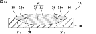
- a terminal electrode 20 is provided on the outer surface of the element body 10.
- the terminal electrode 20 has a first electrode 21 that contacts the outer surface of the element body 10, and a second electrode 22 that covers the surface of the first electrode 21. Details of the first electrode 21 and the second electrode 22 will be described later.
- An insulating layer 30 is provided on the outer surface of the element body 10.
- the insulating layer 30 covers at least a portion of the outer edge 21e of the first electrode 21 and a portion of the outer surface of the element body 10.
- the insulating layer 30 covers the outer edge 21e at both ends of the first electrode 21 and a portion of the outer surface of the element body 10.
- the insulating layer 30 may cover the entire portion of the outer surface of the first electrode 21 that is not covered by the second electrode 22. In other words, the entire outer surface of the first electrode 21 may be covered by the second electrode 22 or the insulating layer 30.
- the first electrode 21, insulating layer 30, and second electrode 22 overlap in this order from the outer surface side of the element body 10.
- the first electrode 21, insulating layer 30, and second electrode 22 overlap in this order from the outer surface side of the element body 10 over the entire portion where the insulating layer 30 covers the first electrode 21.
- the first electrode 21 and second electrode 22 sandwich the insulating layer 30.
- the inner end 31 of the insulating layer 30 contacts the first electrode 21 and the second electrode 22.
- the inner end 31 of the insulating layer 30 is the point where the first electrode 21, the second electrode 22, and the insulating layer 30 contact each other.
- FIG. 2 is a plan view showing a schematic example of a terminal electrode and an insulating layer.
- the insulating layer 30 may contain glass.
- the insulating layer 30 may be a sintered body of glass ceramics.
- the type of glass is not particularly limited, but examples include borosilicate glass and crystallized glass.
- the insulating layer 30 may contain the same glass as that contained in the element body 10.
- the insulating layer 30 may have the same main component as the base body 10.
- the insulating layer 30 may also have the same composition as the base body 10.
- the first electrode 21 and the second electrode 22 are described below.
- the content of the non-conductive component in the first electrode 21 is 3% by weight or more and 40% by weight or less.
- the content of the non-conductive component in the second electrode 22 is 0% by weight or more and 10% by weight or less.
- the content of the non-conductive component in the first electrode 21 is the same as or higher than the content of the non-conductive component in the second electrode 22 .
- the content of non-conductive components means the content of components constituting the electrode excluding conductive components Cu and Ag.
- the content of non-conductive components in the electrode can be calculated by observing the cross section of the electrode using a scanning electron microscope-energy dispersive X-ray spectroscopy (SEM-EDX). Specifically, the content of conductive components is calculated by the following method. First, the weight ratio of each element in the cross section of the electrode is measured by elemental analysis using SEM-EDX. The sum of the weight ratios of each element detected by SEM-EDX, excluding C and O, is taken as the total weight, or 100% by weight. The sum of the weight percentages of Cu and Ag relative to the total weight is the conductive component content, and the remaining percentage obtained by subtracting the weight percentages of Cu and Ag from the total weight is the non-conductive component content.
- SEM-EDX scanning electron microscope-energy dispersive X-ray spectroscopy
- Figure 3 is a cross-sectional view that shows a schematic diagram of how cracks form in the ceramic substrate of the present invention.
- FIG. 3 shows that a crack has occurred between the second electrode 22 and the insulating layer 30 .
- the content of the non-conductive component in the second electrode 22 is 0% by weight or more and 10% by weight or less, the adhesion between the second electrode 22 and the insulating layer 30 is weak.
- stress that peels off the electrode is applied to the ceramic substrate 1, the second electrode 22 and the insulating layer 30 are likely to peel off, and cracks are likely to occur along the boundary between the second electrode 22 and the insulating layer 30.
- the first electrode 21 and the second electrode 22 are in close contact with each other and have high resistance to stress, so that the progress of the crack stops at the inner end 31 of the insulating layer 30. Therefore, the occurrence of cracks that break the internal conductor 40 provided inside the element body 10 is suppressed, and electrical continuity from the terminal electrode 20 to the internal conductor 40 can be ensured. Furthermore, cracks are generated along the boundary between the second electrode 22 and the insulating layer 30, thereby alleviating the stress applied to the terminal electrode 20 and the insulating layer 30, and the thermal stress resistance of the terminal electrode 20 and the insulating layer 30 is improved.
- the adhesion between the first electrode 21 and the element body 10 can be strengthened. This prevents cracks from progressing between the first electrode 21 and the element body 10. This prevents the first electrode 21 from peeling off from the element body 10, and ensures electrical continuity from the terminal electrode 20 to the internal conductor 40.
- the strength of the first electrode 21 itself can be increased. Therefore, cracks that have reached the inner end portion 31 of the insulating layer 30 are prevented from progressing through the inside of the first electrode 21, and electrical continuity from the terminal electrode 20 to the internal conductor 40 can be ensured.
- the content of non-conductive components in the first electrode 21 is the same as or higher than the content of non-conductive components in the second electrode 22, cracks are likely to occur along the boundary between the second electrode 22 and the insulating layer 30.
- the first electrode 21 and the second electrode 22 are in close contact with each other and have high resistance to stress, so the crack stops progressing at the inner end 31 of the insulating layer 30. Therefore, the occurrence of cracks that would break the internal conductor 40 provided inside the element body 10 is suppressed, and electrical conductivity from the terminal electrode 20 to the internal conductor 40 can be ensured.
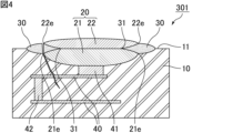
- Figure 4 is a cross-sectional view that shows a schematic diagram of how cracks form in a comparative example ceramic substrate in which the second electrode and the insulating layer have strong adhesion.
- FIG. 4 shows that a crack has occurred that passes through the inside of the insulating layer 30 and the inside of the element body 10 and breaks the internal conductor 40 .
- the content of non-conductive components in the second electrode 22 is higher than 10% by weight. Therefore, the adhesion between the second electrode 22 and the insulating layer 30 is stronger than that of the ceramic substrate 1 shown in FIG. 3.
- the stress is concentrated at the outer edge 22e of the second electrode 22, and a crack that starts from the outer edge 22e of the second electrode 22 and passes through the inside of the insulating layer 30 is likely to occur.
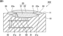
- Figure 5 is a cross-sectional view that shows a schematic diagram of how cracks form in a comparative example ceramic substrate in which the adhesion between the first electrode and the base body is weak.
- FIG. 5 shows that a crack has occurred that passes through the inside of the first electrode 21 and between the first electrode 21 and the element body 10 .
- the content of non-conductive components in the first electrode 21 is less than 3 wt %. Therefore, the adhesion between the first electrode 21 and the element body 10 is weaker than that of the ceramic substrate 1 shown in Fig. 3.
- stress that peels off the electrode is applied to the ceramic substrate 302
- cracks are likely to occur that pass through the inside of the first electrode 21 and between the first electrode 21 and the element body 10. If the first electrode 21 peels off from the element body 10 and the via conductor 41, electrical continuity between the terminal electrode 20 and the internal conductor 40 may be interrupted.
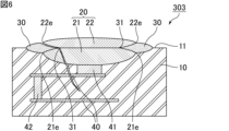
- Figure 6 is a cross-sectional view that shows a schematic diagram of how cracks form in a comparative example ceramic substrate in which the strength of the first electrode itself is low.
- FIG. 6 shows that a crack has occurred that passes through the inside of the first electrode 21 and the inside of the element body 10 and breaks the internal conductor 40 .
- the content of non-conductive components in the first electrode 21 is higher than 40% by weight. Therefore, the strength of the first electrode 21 itself is lower than that of the ceramic substrate 1 shown in Fig. 3.
- a stress that peels off the electrode is applied to the ceramic substrate 303, a crack that reaches the inner end portion 31 of the insulating layer 30 is likely to progress through the inside of the first electrode 21. If the crack progresses into the element body 10 and the internal conductor 40 is broken, there is a risk that electrical continuity from the terminal electrode 20 to the internal conductor 40 will be interrupted.
- the content of the non-conductive component in the first electrode 21 is preferably 5% by weight or more and 20% by weight or less.
- the content of the non-conductive component in the first electrode 21 is more preferably 10% by weight or more and 20% by weight or less.
- the content of the non-conductive component in the first electrode 21 may be 10% by weight or more and 15% by weight or less.
- the content of the non-conductive component in the second electrode 22 is preferably 0.5% by weight or more and 6% by weight or less.
- the content of the non-conductive component in the second electrode 22 is more preferably 0.5% by weight or more and 3% by weight or less.
- the content of non-conductive components in the first electrode 21 is preferably higher than the content of non-conductive components in the second electrode 22. In this case, cracks are more likely to occur along the boundary between the second electrode 22 and the insulating layer 30, so electrical conductivity from the terminal electrode 20 to the internal conductor 40 can be more sufficiently ensured.
- the conductive and non-conductive components contained in the first electrode 21 and the second electrode 22 are described in detail below.
- the first electrode 21 and the second electrode 22 contain Cu or Ag as a conductive component.
- the first electrode 21 and the second electrode 22 may contain only one of Cu and Ag as a conductive component, or may contain both Cu and Ag.
- the first electrode 21 and the second electrode 22 may contain at least one of glass and a filler as a non-conductive component.
- the content of the non-conductive components means the sum of the content of the glass and the content of the filler.
- the glass as the non-conductive component is not particularly limited, but examples include borosilicate glass and crystallized glass.
- the glass as the non-conductive component may be the same glass as that contained in the element body 10, or may be the same glass as that contained in the insulating layer 30. It is preferable that the glass as the non-conductive component is the same glass as that contained in the element body 10 and the insulating layer 30.
- the glass contained in the first electrode 21 or the second electrode 22 strengthens the adhesion between the first electrode 21 or the second electrode 22 and the insulating layer 30.
- glass as a non-conductive component is glass containing 44.0 to 69.0 wt % RO ( R is at least one alkaline earth metal selected from Ba, Ca, and Sr), 14.2 to 30.0 wt % SiO2 , 10.0 to 20.0 wt % B2O3 , 0.5 to 4.0 wt % Al2O3 , 0.3 to 7.5 wt % Li2O , and 0.1 to 5.5 wt % MgO.
- R is at least one alkaline earth metal selected from Ba, Ca, and Sr
- glass as a non-conductive component is glass having a SiO2 content of 15% by weight or more and 65% by weight or less, a B2O3 content of 11% by weight or more and 30 % by weight or less, a weight ratio of SiO2 to B2O3 ( SiO2 / B2O3 ) of 1.21 or more, and a weight ratio of Al2O3 to ZnO ( Al2O3 /ZnO) of 0.75 or more and 1.64 or less.
- the filler as the non -conductive component is not particularly limited, and may be ceramic, for example, ceramics such as Al2O3 , ZrO2 , Mg2SiO4 , and SiO2 .
- the filler as the non-conductive component is preferably ceramic having the same composition as the ceramic contained in the element body 10 and the insulating layer 30.
- the filler contained in the first electrode 21 or the second electrode 22 strengthens the adhesion between the first electrode 21 or the second electrode 22 and the insulating layer 30.
- the content of the non-conductive components in the first electrode 21 and the second electrode 22 may be the sum of the content of the glass and the filler.
- the content of the non-conductive components in the first electrode 21 and the second electrode 22 may be measured by measuring the content of the glass and the filler in the first electrode 21 and the second electrode 22.
- the content of the non-conductive component in the first electrode 21 and the second electrode 22 may be the content of glass.
- the content of the non-conductive component in the first electrode 21 and the second electrode 22 may be measured by measuring the content of glass in the first electrode 21 and the second electrode 22.
- the glass content in the first electrode 21 may be 0 wt % or more and 40 wt % or less, 3 wt % or more and 40 wt % or less, 5 wt % or more and 20 wt % or less, 10 wt % or more and 20 wt % or less, or 10 wt % or more and 15 wt % or less.
- the first electrode 21 may contain only glass as a non-conductive component.
- the filler content in the first electrode 21 may be 0 wt % or more and 40 wt % or less, 3 wt % or more and 40 wt % or less, 5 wt % or more and 20 wt % or less, 10 wt % or more and 20 wt % or less, or 10 wt % or more and 15 wt % or less.
- the first electrode 21 may contain only a filler as the non-conductive component.
- the total of the glass content and the filler content in the first electrode 21 may be 0 wt % or more and 40 wt % or less, or 3 wt % or more and 40 wt % or less, or 5 wt % or more and 20 wt % or less, or 10 wt % or more and 20 wt % or less, or 10 wt % or more and 15 wt % or less.
- the first electrode 21 may contain only glass and a filler as non-conductive components.
- the glass content in the second electrode 22 may be 0 wt % or more and 10 wt % or less, 0.5 wt % or more and 6 wt % or less, or 0.5 wt % or more and 3 wt % or less.
- the second electrode 22 may include only glass as a non-conductive component.
- the filler content in the second electrode 22 may be 0 wt % or more and 10 wt % or less, 0.5 wt % or more and 6 wt % or less, or 0.5 wt % or more and 3 wt % or less.
- the second electrode 22 may contain only a filler as a non-conductive component.
- the sum of the glass content and the filler content in the second electrode 22 may be 0 wt % or more and 10 wt % or less, 0.5 wt % or more and 6 wt % or less, or 0.5 wt % or more and 3 wt % or less.
- the second electrode 22 may contain only glass and a filler as non-conductive components.
- the glass content in the first electrode 21 is preferably the same as or higher than the glass content in the second electrode 22. It is more preferable that the glass content in the first electrode 21 is higher than the glass content in the second electrode 22.
- the sum of the glass content and the filler content in the first electrode 21 is preferably the same as or higher than the sum of the glass content and the filler content in the second electrode 22. It is more preferable that the sum of the glass content and the filler content in the first electrode 21 is higher than the sum of the glass content and the filler content in the second electrode 22.
- the content of non-conductive components can be calculated by measuring the weight ratio of each element in the cross section of the electrode using SEM-EDX. This calculation method estimates the weight ratio of the non-conductive components added when the raw materials for the electrode were prepared from the weight ratio of each element in the electrode after firing. Therefore, the content of non-conductive components in the first electrode 21 and the second electrode 22 may be calculated from the weight ratio of each element when the raw materials were prepared.
- the ratio of the total weight of the glass and the filler to the total weight of Cu, Ag, glass, and filler added when the raw materials are prepared may be calculated as the content of the non-conductive component.
- the ratio of the weight of glass to the total weight of Cu, Ag, and glass added when the raw materials are prepared may be calculated as the content of the non-conductive component.
- the thickness of the first electrode 21 (the length indicated by the double-headed arrow t1 in Figure 1) at the inner end 31 of the insulating layer 30 is the same as or thicker than the thickness of the second electrode 22 (the length indicated by the double-headed arrow t2 in Figure 1).
- the first electrode 21 is thick, the resistance to stress at the inner end 31 of the insulating layer 30 is further increased, so that electrical conductivity from the terminal electrode 20 to the internal conductor 40 can be more sufficiently ensured.
- the thickness of the first electrode 21 (length indicated by double-headed arrow t1 in FIG. 1) at the inner end 31 of the insulating layer 30 is thicker than the thickness of the second electrode 22 (length indicated by double-headed arrow t2 in FIG. 1).
- the thickness of the first electrode 21 (length indicated by double-headed arrow t1 in FIG. 1) may be the same as the thickness of the second electrode 22 (length indicated by double-headed arrow t2 in FIG. 1).
- the thickness of the first electrode 21 at the inner end 31 of the insulating layer 30 (the length indicated by the double-headed arrow t1 in FIG. 1) may be, for example, 5 ⁇ m or more and 20 ⁇ m or less.
- the thickness of the second electrode 22 at the inner end 31 of the insulating layer 30 (the length indicated by the double-headed arrow t2 in FIG. 1) may be, for example, 5 ⁇ m or more and 15 ⁇ m or less.
- the ratio (t1/t2) of the thickness of the first electrode 21 to the thickness of the second electrode 22 at the inner end 31 of the insulating layer 30 is not particularly limited, and may be, for example, 1.0 or more and 4.0 or less, 1.0 or more and 2.0 or less, or greater than 1.0 and 2 or less.
- the outer edge 21e of the first electrode 21 overlaps with the outer edge 22e of the second electrode 22 or is located outside the outer edge 22e of the second electrode 22.
- the entire second electrode 22 overlaps with the first electrode 21.
- the area of the first electrode 21 is the same as or larger than the area of the second electrode 22.
- the concentration of stress on the outer edge portion 22e of the second electrode 22 it is possible to further suppress the occurrence of cracks that pass through the inside of the insulating layer 30 and the inside of the element body 10 and break the internal conductor 40 as shown in FIG. 4. This makes it possible to more sufficiently ensure electrical continuity from the terminal electrode 20 to the internal conductor 40.
- the outer edge 21e of the first electrode 21 overlaps with the outer edge 22e of the second electrode 22. Also, in plan view from the thickness direction perpendicular to the outer surface of the element body 10, the area of the first electrode 21 is the same as the area of the second electrode 22.
- the width of the overlapping portion of the first electrode 21, the insulating layer 30, and the second electrode 22 from the outer surface side of the element body 10 is not particularly limited, but may be, for example, 10 ⁇ m or more and 75 ⁇ m or less. If the width of the overlapping portion of the first electrode 21, the insulating layer 30, and the second electrode 22 in this order is 10 ⁇ m or more, the insulating layer 30 can sufficiently improve the adhesion between the terminal electrode 20 and the element body 10.
- the width of the overlapping portion of the first electrode 21, the insulating layer 30, and the second electrode 22 in this order is small, the distance between the end of the substrate and the electrode and the distance between the electrodes can be made wider.
- the bonding area between the first electrode 21 and the second electrode 22 is increased, so that the bonding between the first electrode 21 and the second electrode 22 can be strengthened.
- the width of the overlapping portion of the first electrode 21, the insulating layer 30, and the second electrode 22 in this order may be, for example, 75 ⁇ m or less.
- the width of the overlapping portion of the first electrode 21, the insulating layer 30, and the second electrode 22 in this order may be 20 ⁇ m or more and 40 ⁇ m or less.
- the width of the overlapping portion of the first electrode 21, the insulating layer 30, and the second electrode 22 in this order may be constant.
- the width of the overlapping portion of the first electrode 21, the insulating layer 30, and the second electrode 22 in this order may be different on each side of the electrode.
- the width of the portion where the insulating layer 30 covers the first electrode 21 is the same as the width of the portion where the first electrode 21, the insulating layer 30, and the second electrode 22 overlap in this order.
- the width of the portion where the insulating layer 30 covers the first electrode 21 may be greater than the width of the portion where the first electrode 21, the insulating layer 30, and the second electrode 22 overlap in this order.
- the width of the portion where the insulating layer 30 covers the first electrode 21 may be 10 ⁇ m or more and 75 ⁇ m or less, or may be 20 ⁇ m or more and 40 ⁇ m or less.
- the first electrode 21 is located inside (lower side in FIG. 1) of a plane including the outer surface 11 of the portion of the outer surface of the element body 10 where the terminal electrode 20 and insulating layer 30 are not provided.
- the first electrode 21 may be located so as to pass through a plane including the outer surface 11 of the portion of the outer surface of the element body 10 where the terminal electrode 20 and insulating layer 30 are not provided.
- the first electrode 21 may also be located outside (upper side in FIG. 1) of a plane including the outer surface 11 of the portion of the outer surface of the element body 10 where the terminal electrode 20 and insulating layer 30 are not provided.
- the outer surface of the second electrode 22 and the outer surface of the insulating layer 30 are located outside (upper side in FIG. 1) the outer surface of the element body 10, but the outer surface 11 of the portion of the outer surface of the element body 10 where the terminal electrode 20 and the insulating layer 30 are not provided, the outer surface of the second electrode 22, and the outer surface of the insulating layer 30 may be flush with each other. Also, the second electrode 22 and the insulating layer 30 may be located inside (lower side in FIG. 1) a plane including the outer surface 11 of the portion of the outer surface of the element body 10 where the terminal electrode 20 and the insulating layer 30 are not provided.
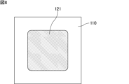
- FIGS. 7A and 7B are cross-sectional and plan views each showing a process of forming a first conductive paste layer that will become a first electrode after firing, respectively.
- internal conductors are not shown in FIGS. 7 to 17, but at least one internal conductor is provided inside the element body.
- the ceramic green sheet 110 is formed by forming a slurry containing, for example, ceramic powder, an organic binder, and a solvent into a sheet using a doctor blade method or the like.
- the above-mentioned slurry may contain various additives such as a dispersant and a plasticizer.
- the materials described as the materials for the base body 10 in the explanation of the ceramic substrate can be used as the materials for the ceramic green sheet 110.
- a first conductive paste layer 121 that will become the first electrode 21 after firing is formed on the ceramic green sheet 110 that is placed on the surface of the electronic component after lamination.
- the first conductive paste layer 121 is formed by patterning using a method such as screen printing or photolithography.
- the area in which the first conductive paste layer 121 is formed can be set appropriately depending on the distance between the electrodes, the distance between the electrodes and the ends of the electronic components, etc.
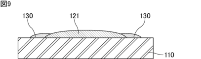
- Figure 9 is a cross-sectional view that shows a schematic of the process of forming an insulating paste layer that will become an insulating layer after firing.
- Figure 10 is a plan view that shows a schematic of the process of forming an insulating paste layer that will become an insulating layer after firing.
- An insulating paste layer 130 which will become the insulating layer 30 after firing, is formed on the outer edge of the first conductive paste layer 121.
- the insulating paste layer 130 is also formed continuously on the ceramic green sheet 110 where the first conductive paste layer 121 is not formed.
- the insulating paste layer 130 is formed by forming a pattern using a method such as screen printing.
- the width of the overlapping portion between the insulating paste layer 130 and the first conductive paste layer 121 (the length indicated by the double-headed arrow w1' in FIG. 10) can be set appropriately. If the width of the overlapping portion between the insulating paste layer 130 and the first conductive paste layer 121 is large, the insulating layer 30 can sufficiently improve the adhesion between the first electrode 21 and the base body 10 after firing. If the width of the overlapping portion between the insulating paste layer 130 and the first conductive paste layer 121 is small, the bonding area between the first conductive paste layer 121 and the second conductive paste layer 122 described later becomes large, so that the bonding between the first electrode 21 and the second electrode 22 after firing can be strengthened. From these viewpoints, the width of the overlapping portion between the insulating paste layer 130 and the first conductive paste layer 121 may be 10 ⁇ m or more and 75 ⁇ m or less, or 20 ⁇ m or more and 40 ⁇ m or less.
- FIG. 11 is a cross-sectional view that shows a schematic process of forming a second conductive paste layer that will become the second electrode after firing.
- FIG. 12 is a plan view that shows a schematic process of forming a second conductive paste layer that will become the second electrode after firing.
- the second conductive paste layer 122 which will become the second electrode 22 after firing, is formed on the first conductive paste layer 121 and the insulating paste layer 130.
- the second conductive paste layer 122 is formed so as to cover the entire exposed portion of the first conductive paste layer 121.
- the second conductive paste layer 122 is also formed so as to cover a portion of the exposed portion of the insulating paste layer 130.
- the area in which the second conductive paste layer 122 is formed is determined appropriately based on the product specifications, etc. It is preferable that the area in which the second conductive paste layer 122 is formed is the same as the area in which the first conductive paste layer 121 is formed, or is smaller than the area in which the first conductive paste layer 121 is formed.
- holes for forming via conductors are formed in the specific ceramic green sheet 110.
- the holes can be formed, for example, by laser processing.
- a conductive paste is applied in a desired shape to each surface of the specific ceramic green sheet 110 to form a conductive paste layer that will become an internal conductor after firing.
- the conductive paste layer can be formed by a method such as screen printing using a conductive paste that contains, for example, Cu or Ag as a conductive component.
- the conductive paste is filled into the holes for forming the via conductors to form a conductive paste body that will become a via conductor after firing. In this way, electrodes that become the inductance elements and capacitance elements that constitute the LC filter can be formed.
- the outer surface 11 of the portion of the outer surface of the element body 10 where the terminal electrode 20 and the insulating layer 30 are not provided, the outer surface of the second electrode 22, and the outer surface of the insulating layer 30 may be flush with each other in the ceramic substrate 1 after firing.
- the unfired laminate may be cut into individual chips using a dicer or microcutter.
- the surface of the unsintered laminate may be barrel polished.
- the unsintered laminate is enclosed in a small box called a barrel together with media balls that are harder than the material of the base body 10, and polishing is performed by rotating the barrel. Barrel polishing rounds the corners and ridges of the unsintered laminate.
- the unsintered laminate is sintered to obtain an electronic component equipped with the ceramic substrate of the present invention.
- the sintering temperature is not particularly limited, but is preferably, for example, 800°C or higher and 1000°C or lower.
- the sintering atmosphere is not particularly limited, and examples include a nitrogen atmosphere. However, if the electrode material does not oxidize, an air atmosphere may be used.
- the first conductive paste layer 121, the second conductive paste layer 122, and the insulating paste layer 130 are fired simultaneously, but firing may also be performed in a state where only the first conductive paste layer 121 and the insulating paste layer 130 have been formed (the state shown in Figures 9 and 10).
- the second conductive paste layer 122 may be formed so as to cover the fired first electrode 21, and then a heat treatment for baking may be performed to form the second electrode 22.
- FIG. 13 is a cross-sectional view showing a schematic diagram of a first modified example of a ceramic substrate.
- the outer edge 21e of the first electrode 21 is positioned outside the outer edge 22e of the second electrode 22.
- the area of the first electrode 21 is larger than the area of the second electrode 22 when viewed from the thickness direction.
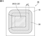
- FIG. 14 is a cross-sectional view that shows a schematic representation of a second modified example of a ceramic substrate.
- FIG. 15 is a plan view that shows a schematic representation of a second modified example of a ceramic substrate.
- the insulating layer 30 partially covers the outer surface of the second electrode 22.
- in Figure 14 in the thickness direction (vertical direction in Figure 14) perpendicular to the outer surface of the element body 10, there is a portion (part indicated by double arrow w2 in Figure 14) where the first electrode 21, insulating layer 30, second electrode 22, and insulating layer 30 overlap in this order from the outer surface side of the element body 10.
- part of the insulating layer 30 is sandwiched between the first electrode 21 and the second electrode 22, and part of the insulating layer 30 covers the outer surface of the second electrode 22.
- the width of the portion where the insulating layer 30 covers the outer surface of the second electrode 22 is the same as the width of the portion where the first electrode 21, the insulating layer 30, and the second electrode 22 are overlapped in that order from the outer surface side of the base body 10.
- the width of the portion where the insulating layer 30 covers the outer surface of the second electrode 22 may be larger or smaller than the width of the portion where the first electrode 21, the insulating layer 30, and the second electrode 22 are overlapped in that order from the outer surface side of the base body 10.
- the overlapping portions of the first electrode 21, insulating layer 30, second electrode 22, and insulating layer 30 from the outer surface side of the element body 10 may be present on three sides of the terminal electrode 20.
- the overlapping portions of the first electrode 21, insulating layer 30, second electrode 22, and insulating layer 30 from the outer surface side of the element body 10 may be present on all sides of the terminal electrode 20.
- the insulating layer 30 partially covers the outer surface of the second electrode 22.
- the first electrode 21, the second electrode 22, and the insulating layer 30 overlap in this order from the outer surface side of the element body 10.
- the insulating layer 30 is not sandwiched between the first electrode 21 and the second electrode 22.
- the first electrode 21, the second electrode 22, and the insulating layer 30 may overlap in this order from the outer surface side of the element body 10 on three sides of the terminal electrode 20.
- an LC filter in which an inductance element and a capacitance element are formed by an internal conductor provided inside the ceramic substrate body will be described.
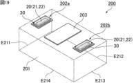
- FIG. 18 is a perspective view that shows a schematic example of an electronic component of the present invention.
- FIG. 19 is a perspective view that shows a schematic example of an input/output terminal and a ground terminal in an example of an electronic component of the present invention.
- FIG. 20 is an exploded perspective view that shows a schematic example of an electronic component of the present invention.
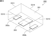
- the laminated LC filter 200 comprises a base body 201.
- an input/output terminal 202a, an input/output terminal 202b, and a ground terminal 203 are formed on the lower main surface of the element body 201.
- the input/output terminals 202a and 202b include a terminal electrode 20 and an insulating layer 30.
- the details of the terminal electrode 20 and the insulating layer 30 are not shown, but the configurations of the terminal electrode 20 and the insulating layer 30 are the same as those of the terminal electrode 20 and the insulating layer 30 in the ceramic substrate 1 shown in FIG. 1, FIG. 2, and FIG. 3.
- the ground terminal 203 does not include the terminal electrode 20 and the insulating layer 30, but the ground terminal 203 may include the terminal electrode 20 and the insulating layer 30.
- the configurations of the terminal electrode 20 and the insulating layer 30 may be the same as those of the terminal electrode 20 and the insulating layer 30 in the ceramic substrate 1 shown in FIG. 1, FIG. 2, and FIG. 3.
- the base body 201 is made up of eight dielectric layers 201a to 201h, made of ceramic or the like, stacked in order from the bottom up.
- the element body 201 has a first side E211, a second side E212, a third side E213, and a fourth side E214, which are connected in order.
- Input/output terminals 202a, 202b, and a ground terminal 203 are formed on the lower main surface of dielectric layer 201a.
- a ground conductor pattern 204 is formed on the upper main surface of the dielectric layer 201a.
- the ground conductor pattern 204 is connected to the ground terminal 203 by via conductors 205a to 205e.
- via conductors 205f-205l are formed penetrating between the upper and lower principal surfaces of the dielectric layer 201b.
- the via conductors 205f-205j are depicted as extending further downward than they actually are (the same applies to the via conductors described below) so that the connection relationship can be seen.
- the via conductors 205f-205l are each connected to the ground conductor pattern 204.
- the capacitor conductor pattern 206a is connected to the input/output terminal 202a through a via conductor 207a.
- the capacitor conductor pattern 206e is connected to the input/output terminal 202b through a via conductor 207b.
- the via conductor 207a and the via conductor 207b correspond to the via conductor 41 connected to the first electrode 21 in FIG.
- via conductors 205f-205l are formed between the upper and lower main surfaces of the dielectric layer 201c. As described above, the via conductors 205f-205l are also formed in the dielectric layer 201b, but the via conductors with the same reference number formed in different dielectric layers are connected to each other. Eight other via conductors 205m-205t are formed between the upper and lower main surfaces of the dielectric layer 201c.
- the via conductors 205m and 205n are each connected to the capacitor conductor pattern 206a.
- the via conductor 205o is connected to the capacitor conductor pattern 206b.
- the via conductors 205p and 205q are each connected to the capacitor conductor pattern 206c.
- the via conductor 205r is connected to the capacitor conductor pattern 206d.
- the via conductors 205s and 205t are each connected to the capacitor conductor pattern 206e.
- Two capacitor conductor patterns 206f and 206g are formed on the upper main surface of the dielectric layer 201c.
- the capacitor conductor pattern 206f is connected to the via conductors 205m and 205n.
- the capacitor conductor pattern 206g is connected to the via conductors 205s and 205t.
- Two capacitor conductor patterns 206h and 206i are formed on the upper main surface of the dielectric layer 201d.
- the capacitor conductor pattern 206h and the capacitor conductor pattern 206i are connected to each other.
- Each of the line-like conductor patterns 217a to 217e includes at least one side that is not parallel to any of the first side E211, second side E212, third side E213, and fourth side E214 of the base body 201.
- One via conductor 205f is connected to the end of the line-like conductor pattern 217a on the second side E212 side, and two via conductors 205m and 205n are connected to the end of the line-like conductor pattern 217a on the fourth side E214 side.
- Two via conductors 205g and 205h are connected to the end of the line-like conductor pattern 217b on the second side E212 side, and one via conductor 205o is connected to the end of the line-like conductor pattern 217b on the fourth side E214 side.
- One via conductor 205i is connected to the end of the line-like conductor pattern 217c on the second side E212 side, and two via conductors 205p and 205q are connected to the end of the line-like conductor pattern 217c on the fourth side E214 side.
- Two via conductors 205j and 205k are connected to the end of the line-shaped conductor pattern 217d on the second side E212 side, and one via conductor 205r is connected to the end of the line-shaped conductor pattern 217d on the fourth side E214 side.
- One via conductor 205l is connected to the end of the line-shaped conductor pattern 217e on the second side E212 side, and two via conductors 205s and 205t are connected to the end of the line-shaped conductor pattern 217e on the fourth side E214 side.
- the laminated LC filter 200 uses space as efficiently as possible and connects as many via conductors 205f-205t as possible to the line-like conductor patterns 217a-217e to reduce internal resistance.
- the line-shaped conductor patterns 227a to 227e have the same shape as the line-shaped conductor patterns 217a to 217e formed on the upper main surface of the dielectric layer 201e.
- via conductors 205f to 205t are connected to the line-shaped conductor patterns 227a to 227e at the same positions as the line-shaped conductor patterns 217a to 217e.
- the line-shaped conductor patterns 237a to 237e have the same shape as the line-shaped conductor patterns 217a to 217e formed on the upper main surface of the dielectric layer 201e.
- via conductors 205f to 205t are connected to the line-shaped conductor patterns 237a to 237e at the same positions as the line-shaped conductor patterns 217a to 217e.
- the dielectric layer 201h is a protective layer.
- the laminated LC filter 200 having the above structure can be manufactured using materials and manufacturing methods that have been widely used in conventional laminated LC filters.
- LC filters of Samples No. 1 to No. 22 were fabricated based on the manufacturing method of electronic components (LC filters) described with reference to Figures 7 to 12 of this specification.
- an internal conductor was formed inside the element body, and the internal conductor formed an inductance element and a capacitance element.
- materials for the first conductive paste layer and the second conductive paste layer were used such that the contents of non-conductive components in the first electrode and the second electrode were the values shown in Table 2.
- RO R is at least one alkaline earth metal selected from Ba, Ca, and Sr
- SiO 2 -B 2 O 3 -Al 2 O 3 -Li 2 O-MgO-based glass was used as the non-conductive component.
- the LC filter of sample No. 19 was manufactured without forming a second conductive paste layer during the manufacturing process.
- the LC filter of sample No. 19 does not include a second electrode.
- the LC filter of sample No. 20 was manufactured without forming a second conductive paste layer and an insulating paste layer during the manufacturing process.
- the LC filter of sample No. 20 does not include a second electrode and an insulating layer.
- the LC filters of samples No. 1 to No. 22 were manufactured under the same conditions except for the above.
- Samples No. 1, No. 2, No. 5, No. 9, No. 13, No. 14, and No. 17 to No. 21 marked with an * in Table 2 are electronic components (LC filters) of comparative examples, not electronic components (LC filters) including the ceramic substrate of the present invention.
- the electronic component (LC filter) of the present invention has electrical continuity marked with ⁇ or ⁇ , confirming that electrical continuity is ensured from the terminal electrodes to the internal conductor.
- An element including a ceramic layer; At least one internal conductor provided inside the element body; a terminal electrode provided on an outer surface of the element body; an insulating layer provided on an outer surface of the element body, the internal conductor and the terminal electrode are electrically connected to each other, the terminal electrode has a first electrode in contact with an outer surface of the element body and a second electrode covering a surface of the first electrode; the insulating layer covers at least a part of an outer edge of the first electrode and a part of an outer surface of the element body; a portion in which the first electrode, the insulating layer, and the second electrode are overlapped in this order from the outer surface side of the element body in a thickness direction perpendicular to the outer surface of the element body,
- the content of the non-conductive component in the first electrode is 3% by weight or more and 40% by weight or less
- the content of the non-conductive component in the second electrode is 0% by weight or more and 10% by weight or less
- a ceramic substrate wherein the content of the non-conductive component in the first electrode
- ⁇ 2> The ceramic substrate according to ⁇ 1>, wherein the content of the non-conductive component in the first electrode is 10% by weight or more and 20% by weight or less.
- ⁇ 3> The ceramic substrate according to ⁇ 1> or ⁇ 2>, wherein the content of the non-conductive component in the second electrode is 0% by weight or more and 6% by weight or less.
- ⁇ 4> In a cross-sectional view of a portion in which the first electrode, the insulating layer, and the second electrode are overlapped in this order from an outer surface side of the element body in the thickness direction, The ceramic substrate according to any one of ⁇ 1> to ⁇ 3>, wherein a thickness of the first electrode at an inner end of the insulating layer is equal to or greater than a thickness of the second electrode.
- ⁇ 5> In a plan view seen from the thickness direction, The ceramic substrate according to any one of ⁇ 1> to ⁇ 4>, wherein an area of the first electrode is equal to or larger than an area of the second electrode.
- ⁇ 6> The ceramic substrate according to any one of ⁇ 1> to ⁇ 5>, wherein the internal conductor includes a via conductor connected to the first electrode.
- ⁇ 7> An electronic component comprising the ceramic substrate according to any one of ⁇ 1> to ⁇ 6>.
Landscapes
- Engineering & Computer Science (AREA)
- Microelectronics & Electronic Packaging (AREA)
- Chemical & Material Sciences (AREA)
- Ceramic Engineering (AREA)
- Inorganic Chemistry (AREA)
- Manufacturing & Machinery (AREA)
- Fixed Capacitors And Capacitor Manufacturing Machines (AREA)
Priority Applications (3)
| Application Number | Priority Date | Filing Date | Title |
|---|---|---|---|
| CN202480052810.3A CN121729988A (zh) | 2023-08-23 | 2024-05-13 | 陶瓷基板和电子部件 |
| JP2025541301A JPWO2025041384A1 (https=) | 2023-08-23 | 2024-05-13 | |
| US19/407,503 US20260089838A1 (en) | 2023-08-23 | 2025-12-03 | Ceramic substrate and electronic component |
Applications Claiming Priority (2)
| Application Number | Priority Date | Filing Date | Title |
|---|---|---|---|
| JP2023-135597 | 2023-08-23 | ||
| JP2023135597 | 2023-08-23 |
Related Child Applications (1)
| Application Number | Title | Priority Date | Filing Date |
|---|---|---|---|
| US19/407,503 Continuation US20260089838A1 (en) | 2023-08-23 | 2025-12-03 | Ceramic substrate and electronic component |
Publications (1)
| Publication Number | Publication Date |
|---|---|
| WO2025041384A1 true WO2025041384A1 (ja) | 2025-02-27 |
Family
ID=94731848
Family Applications (1)
| Application Number | Title | Priority Date | Filing Date |
|---|---|---|---|
| PCT/JP2024/017566 Pending WO2025041384A1 (ja) | 2023-08-23 | 2024-05-13 | セラミック基板及び電子部品 |
Country Status (4)
| Country | Link |
|---|---|
| US (1) | US20260089838A1 (https=) |
| JP (1) | JPWO2025041384A1 (https=) |
| CN (1) | CN121729988A (https=) |
| WO (1) | WO2025041384A1 (https=) |
Citations (5)
| Publication number | Priority date | Publication date | Assignee | Title |
|---|---|---|---|---|
| JPH08172273A (ja) * | 1994-12-16 | 1996-07-02 | Hitachi Ltd | セラミック配線基板及びその実装構造体 |
| JP2013214721A (ja) * | 2012-03-05 | 2013-10-17 | Kyocera Corp | 配線基板 |
| JP2014143361A (ja) * | 2013-01-25 | 2014-08-07 | Kyocera Corp | セラミック配線基板 |
| JP2019125606A (ja) * | 2018-01-11 | 2019-07-25 | 株式会社村田製作所 | 積層コイル部品 |
| JP2022156320A (ja) * | 2021-03-31 | 2022-10-14 | Tdk株式会社 | 積層電子部品 |
-
2024
- 2024-05-13 JP JP2025541301A patent/JPWO2025041384A1/ja active Pending
- 2024-05-13 CN CN202480052810.3A patent/CN121729988A/zh active Pending
- 2024-05-13 WO PCT/JP2024/017566 patent/WO2025041384A1/ja active Pending
-
2025
- 2025-12-03 US US19/407,503 patent/US20260089838A1/en active Pending
Patent Citations (5)
| Publication number | Priority date | Publication date | Assignee | Title |
|---|---|---|---|---|
| JPH08172273A (ja) * | 1994-12-16 | 1996-07-02 | Hitachi Ltd | セラミック配線基板及びその実装構造体 |
| JP2013214721A (ja) * | 2012-03-05 | 2013-10-17 | Kyocera Corp | 配線基板 |
| JP2014143361A (ja) * | 2013-01-25 | 2014-08-07 | Kyocera Corp | セラミック配線基板 |
| JP2019125606A (ja) * | 2018-01-11 | 2019-07-25 | 株式会社村田製作所 | 積層コイル部品 |
| JP2022156320A (ja) * | 2021-03-31 | 2022-10-14 | Tdk株式会社 | 積層電子部品 |
Also Published As
| Publication number | Publication date |
|---|---|
| CN121729988A (zh) | 2026-03-24 |
| US20260089838A1 (en) | 2026-03-26 |
| JPWO2025041384A1 (https=) | 2025-02-27 |
Similar Documents
| Publication | Publication Date | Title |
|---|---|---|
| JP4957723B2 (ja) | 多層セラミック基板およびその製造方法ならびに電子部品 | |
| KR100272647B1 (ko) | 다층세라믹부품의 제조방법 및 다층세라믹부품 | |
| EP1074524B1 (en) | Glass-ceramic composition, circuit substrate using the same and manufacture method thereof | |
| US10626054B2 (en) | Multilayer ceramic substrate and method for manufacturing multilayer ceramic substrate | |
| JP2009152489A (ja) | セラミック多層部品 | |
| JP2010147098A (ja) | 電子部品 | |
| JP2005322743A (ja) | 積層コイル部品の製造方法 | |
| JP3897472B2 (ja) | 受動部品内蔵多層配線基板およびその製造方法 | |
| WO2025041384A1 (ja) | セラミック基板及び電子部品 | |
| KR100439677B1 (ko) | 다층 기판 및 그의 제조방법 | |
| JP4279869B2 (ja) | 多層セラミックス基板 | |
| JP3726359B2 (ja) | 複合積層セラミック部品 | |
| JPH11330705A (ja) | コンデンサ内蔵基板およびその製造方法 | |
| JP2008186909A (ja) | セラミック多層基板 | |
| JP4693284B2 (ja) | 多層配線基板およびその製造方法 | |
| JP5591055B2 (ja) | ガラスセラミック基板およびコイル内蔵ガラスセラミック配線基板 | |
| JP2010153554A (ja) | セラミック基板及びその製造方法 | |
| EP1184882A1 (en) | Conductor pattern built in multilayer board, multilayer board having built-in conductor pattern, and method of manufacturing multilayer board | |
| JPH11284296A (ja) | 配線基板 | |
| JP4814703B2 (ja) | 回路基板 | |
| JP2003046253A (ja) | 多層回路基板 | |
| JP2009010141A (ja) | セラミック多層基板 | |
| JP2009181987A (ja) | セラミック多層基板の製造方法 | |
| JP4869005B2 (ja) | 多層基板の製造方法 | |
| JP2008159726A (ja) | 多層配線基板 |
Legal Events
| Date | Code | Title | Description |
|---|---|---|---|
| 121 | Ep: the epo has been informed by wipo that ep was designated in this application |
Ref document number: 24856080 Country of ref document: EP Kind code of ref document: A1 |
|
| ENP | Entry into the national phase |
Ref document number: 2025541301 Country of ref document: JP Kind code of ref document: A |
|
| NENP | Non-entry into the national phase |
Ref country code: DE |