WO2025004191A1 - 荷電粒子線装置 - Google Patents
荷電粒子線装置 Download PDFInfo
- Publication number
- WO2025004191A1 WO2025004191A1 PCT/JP2023/023832 JP2023023832W WO2025004191A1 WO 2025004191 A1 WO2025004191 A1 WO 2025004191A1 JP 2023023832 W JP2023023832 W JP 2023023832W WO 2025004191 A1 WO2025004191 A1 WO 2025004191A1
- Authority
- WO
- WIPO (PCT)
- Prior art keywords
- charged particle
- particle beam
- beam device
- patterns
- calculation unit
- Prior art date
- Legal status (The legal status is an assumption and is not a legal conclusion. Google has not performed a legal analysis and makes no representation as to the accuracy of the status listed.)
- Ceased
Links
Images






Classifications
-
- H—ELECTRICITY
- H01—ELECTRIC ELEMENTS
- H01J—ELECTRIC DISCHARGE TUBES OR DISCHARGE LAMPS
- H01J37/00—Discharge tubes with provision for introducing objects or material to be exposed to the discharge, e.g. for the purpose of examination or processing thereof
- H01J37/26—Electron or ion microscopes; Electron or ion diffraction tubes
- H01J37/28—Electron or ion microscopes; Electron or ion diffraction tubes with scanning beams
-
- H—ELECTRICITY
- H01—ELECTRIC ELEMENTS
- H01J—ELECTRIC DISCHARGE TUBES OR DISCHARGE LAMPS
- H01J37/00—Discharge tubes with provision for introducing objects or material to be exposed to the discharge, e.g. for the purpose of examination or processing thereof
- H01J37/02—Details
- H01J37/04—Arrangements of electrodes and associated parts for generating or controlling the discharge, e.g. electron-optical arrangement or ion-optical arrangement
- H01J37/147—Arrangements for directing or deflecting the discharge along a desired path
- H01J37/1472—Deflecting along given lines
- H01J37/1474—Scanning means
-
- H—ELECTRICITY
- H01—ELECTRIC ELEMENTS
- H01J—ELECTRIC DISCHARGE TUBES OR DISCHARGE LAMPS
- H01J37/00—Discharge tubes with provision for introducing objects or material to be exposed to the discharge, e.g. for the purpose of examination or processing thereof
- H01J37/02—Details
- H01J37/244—Detectors; Associated components or circuits therefor
Definitions
- the present invention relates to a charged particle beam device.
- Scanning electron microscopes are devices that detect electrons emitted from a sample, and by detecting these electrons, they generate a signal waveform and measure the dimensions between peaks (pattern edges), for example.
- Patent Document 1 describes a charged particle beam irradiation method in which, in order to suppress non-uniform charging of a sample in which a preliminary irradiation area contains multiple different materials or in which the pattern density in the preliminary irradiation area varies depending on the position, the preliminary irradiation area is divided into multiple areas and charged using a beam with different beam irradiation conditions.
- This technology requires area division, so there is a concern that it may reduce throughput. Furthermore, there is no description of a method for imaging without preliminary irradiation.
- Patent Document 2 when acquiring an image of the FOV (field of view), spaced beam irradiation points are set.
- the deflector is controlled to scan the charged particle beam faster when irradiating a position on the sample between each irradiation point than when irradiating the charged particle beam to a position on the sample corresponding to each irradiation point (a position on the sample corresponding to each pixel where signal detection is performed).
- This describes a method that can mitigate and control the effects of charging in a minute area that occurs within the FOV.
- Patent Document 2 describes charging differences in a minute area, but does not describe imaging including multiple patterns.
- Patent Document 1 When imaging multiple patterns with charged particle beam devices, shading and distortion caused by differences in charge between patterns are an issue.
- Patent Document 1 a method has been proposed for dividing an area and creating an image under different imaging conditions, but a method for imaging different patterns at the same time under conditions that do not create differences in charge has not been disclosed.
- Patent Document 2 a method has been proposed for avoiding charging in small areas by adjusting the irradiation point and scanning speed, but this is not disclosed for cases involving multiple patterns. From the above, it is desirable to be able to capture images containing multiple patterns without preliminary irradiation or area division, and to achieve this, simultaneous control of the charge of multiple patterns is necessary.
- the present invention provides a charged particle beam device that can avoid shading or distortion caused by differences in charge between patterns and improve throughput.
- the charged particle beam device includes a scanning deflector that scans a charged particle beam emitted from a charged particle source, a signal electron deflector that deflects the trajectory of signal electrons emitted from a sample, a detector that detects signal electrons obtained based on the scanning of the charged particle beam, and a pull-up electrode that pulls up the signal electrons to the detector, and has a calculation unit that, when imaging an area including multiple patterns, determines imaging conditions that result in a uniform distribution of measurement values for multiple patterns based on a combination of at least two of the control parameters irradiation current density, pull-up electric field, acceleration voltage, magnification, scan method, and scan rotation.
- FIG. 13 is a diagram showing an example of the relationship between the pull-up electric field and the charging potential when the irradiation current is changed.
- FIG. 13 is a diagram showing an example of a database of control parameters and charging potentials.
- FIG. 13 is a diagram illustrating an example of a GUI.
- FIG. 13 is a diagram showing an example in which three different patterns exist.
- FIG. 13 is a diagram showing the relationship between the irradiation current and the charging potential for each pattern before adjustment.
- FIG. 13 is a diagram showing the relationship between the projection current and the charging potential for each pattern after the acceleration voltage is adjusted.
- FIG. 13 is a diagram showing the relationship between the projection current and the charging potential for each pattern after adjusting the acceleration voltage and the pull-up electric field.
- FIGS. 13A and 13B are diagrams showing an example of distribution of two-dimensional pattern shapes in a review SEM according to the second embodiment of the present invention.
- FIG. 11 is a diagram showing a schematic configuration of a multi-beam SEM according to a third embodiment of the present invention.
- FIG. 1 is a diagram showing a schematic configuration of a scanning electron microscope (SEM) 100 which is a charged particle beam device according to this embodiment.
- the scanning electron microscope 100 includes, as its main components, an electron gun 101, a condenser lens 103, a primary electron deflector (scanning deflector) 104, an objective lens 105, a signal electron deflector 107, a condenser lens (lens for adjusting the aperture angle) 108, a detector 109, a signal electron aperture 110, a signal electron deflector 111, a detector 113, a calculation unit 114, and a storage unit 115.
- SEM scanning electron microscope
- the scanning electron microscope 100 also has a display unit for receiving input from a user and displaying various parameters and observation patterns.
- the calculation unit 114 is realized by, for example, a processor such as a CPU (not shown), a ROM for storing various programs, a RAM for temporarily storing data in the calculation process, and a storage unit such as an external storage unit, and the processor such as the CPU reads and executes various programs stored in the ROM, and stores the calculation results, which are the execution results, in the RAM, the external storage unit, or cloud storage via a network connection or the like.
- the electrons passing through the signal electron aperture 110 are deflected by the signal electron deflector 111 toward the detector 113 and detected by the detector 113.
- some scanning electron microscopes are provided with an energy filter 112 capable of discriminating signal electrons according to energy in front of the detector 113, and the detector 113 detects the electrons that have passed through the energy filter 112. It is possible to estimate the charged state of the sample 106 from the change in the signal amount when the voltage applied to the energy filter 112 is changed.
- the charge measurement using the energy filter 112 takes time, and is not realistic for aiming for a high throughput measurement of 1 cm 2 /hr or more in the future.
- the calculation unit 114 executes the control of each optical element included in the scanning electron microscope 100, the control of the voltage applied to the energy filter 112, the control of the deflection amount of the signal electron deflector 107, the calculation of the composite ratio of the signals detected by the detectors 109 and 113, and the like.
- the calculation unit 114 also creates an observation image of the sample 106 using the detection signal of the signal electrons detected by the detectors 109 and 113.
- the storage unit 115 is a storage device that stores data used by the calculation unit 114. For example, as shown in FIG. 10, a database (DB) of observation conditions and charging potential for each pattern can be stored.
- DB database
- the calculation unit 114 determines imaging conditions such as irradiation current density, pulling electric field, acceleration voltage, scanning method, and scan rotation based on the database (DB) stored in the image memory. Note that a configuration in which another calculation device is provided instead of the calculation unit 114 and determines the imaging conditions may be adopted. Also, even if there is no database (DB), it is possible to experimentally determine the imaging conditions.
- DB database
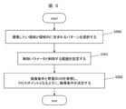
- step S300 an area to be imaged and a pattern to be included in the area are selected.
- a case where two types of patterns, pattern A and pattern B, are mixed is considered.
- step S301 the control parameters and the range to be controlled are set.
- the control parameters are set to the irradiation current and the pull-up electric field, and the control range of each parameter is set to 8 pA to 500 pA (irradiation current) and 2 kV/mm to 4 kV/mm (pull-up electric field).
- step S500 first select the area to be imaged and the pattern included in the area. As in the case of FIG. 3 described above, consider the case where two types of patterns, pattern A and pattern B, are mixed.
- step 501 the control parameters and the range to be controlled are set.
- the database (DB) shown in FIG. 4 is referenced, and imaging conditions that will result in a uniform distribution of length measurement values for multiple patterns are presented (step S502). At this time, there is no need to change the observation conditions and check the length measurement value distribution as described above, and the cross point between the contour lines that results in a uniform length measurement value for each pattern becomes the optimal condition.
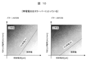
- FIG. 10 is a diagram showing an example of a database of control parameters and charging potential.
- a database DB
- DB database
- the probe current and the pulling electric field are selected as the control parameters, a zero charging contour line is created for each pattern.
- the cross points of these contour lines are the optimal conditions. Since it takes time to obtain data for all points when creating a database (DB), it is possible to obtain data for only a few points and calculate the remaining data from the obtained data. Since the sample potential changes linearly with respect to the pulling electric field, it can be inferred from the slope if at least two points are obtained. It is also possible to estimate using simulation.
- Fig. 11 is a diagram showing an example of a GUI. As shown in Fig.
- multiple patterns of charging control require optimization of multiple parameters such as the irradiation current and the pull-up electric field. If the pull-up voltage also serves as a deceleration voltage for the primary electrons, changing the pull-up electric field will change the conditions of the primary optical system, which may affect the magnification and Rot. In this case, feedback is sent to the primary electron deflector 104 to readjust the primary optical conditions.
- Figure 12 shows an example where there are three different patterns.
- the three different patterns include a fine line & space pattern A1400, a coarse line & space pattern B1401, and a patternless pattern C1402.
- Figure 13 shows the relationship between the irradiation current and the charge potential of each pattern before adjustment.
- the irradiation current value at which the charge potential reverses from positive to negative is small in the order of pattern A ⁇ pattern B ⁇ pattern C. The reason is that the more patterns there are, the more likely it is that a positive charge will be formed locally, and return electrons will be generated.
- Figure 14 shows the relationship between the irradiation current and the charge potential of each pattern after adjusting the acceleration voltage.
- the cross points of the three patterns that is, patterns A, B, and C
- the pull-up electric field it is possible to adjust the cross points so that they overlap with the zero charge, and achieve simultaneous zero charge of the three patterns.
- four independent charge control parameters are required.
- An example of a charge control parameter that is independent of the acceleration voltage, the irradiation current, and the pull-up electric field is the observation magnification.
- this embodiment makes it possible to provide a charged particle beam device that can avoid shading or distortion caused by charge differences between patterns and improve throughput.
- an example assuming an inspection SEM (review SEM) will be described.
- the device configuration of the review SEM is basically the same as that shown in Fig. 1, but the inspection flow is different from that of the critical dimension SEM (CD-SEM), in that the location of the defect is roughly identified by an optical inspection device, and then a detailed inspection is performed by an electron microscope (SEM). Therefore, instead of simultaneously imaging multiple patterns, the conditions are set in advance so that the charge of multiple patterns contained in the wafer (sample 106) to be inspected is all zero, and it is possible to reduce inspection omissions due to uneven brightness or distortion.
- CD-SEM critical dimension SEM
- Figure 16 shows an example of a two-dimensional pattern shape distribution. As shown in the right diagram of Figure 16, with zero charge, the pattern is made up of a row of perfect circles of equal size, but with positive charge, as shown in the left diagram of Figure 16, the outer circle has an ellipse. When determining imaging conditions experimentally, it is best to set the optical conditions so that the pattern shape is the same at all positions.
- FIG. 17 is a diagram showing a schematic configuration of a multi-beam SEM 1300 which is a charged particle beam device according to this embodiment.
- the same components as those shown in FIG. 1 are denoted by the same reference numerals, and duplicated explanations will be omitted below.
- a beam splitter 1301 is provided in the middle of the trajectory of the primary electrons to split the primary beam (electron beam 102).
- the present invention is not limited to the above-described embodiments, but includes various modified examples.
- the above-described embodiments have been described in detail to clearly explain the present invention, and the present invention is not necessarily limited to those having all of the configurations described. It is also possible to replace part of the configuration of one embodiment with the configuration of another embodiment, and it is also possible to add the configuration of another embodiment to the configuration of one embodiment.
Landscapes
- Chemical & Material Sciences (AREA)
- Analytical Chemistry (AREA)
- Testing Or Measuring Of Semiconductors Or The Like (AREA)
Priority Applications (4)
| Application Number | Priority Date | Filing Date | Title |
|---|---|---|---|
| PCT/JP2023/023832 WO2025004191A1 (ja) | 2023-06-27 | 2023-06-27 | 荷電粒子線装置 |
| KR1020257030052A KR20250150034A (ko) | 2023-06-27 | 2023-06-27 | 하전 입자선 장치 |
| JP2025529055A JPWO2025004191A1 (https=) | 2023-06-27 | 2023-06-27 | |
| TW113119931A TWI908100B (zh) | 2023-06-27 | 2024-05-30 | 荷電粒子束裝置 |
Applications Claiming Priority (1)
| Application Number | Priority Date | Filing Date | Title |
|---|---|---|---|
| PCT/JP2023/023832 WO2025004191A1 (ja) | 2023-06-27 | 2023-06-27 | 荷電粒子線装置 |
Publications (1)
| Publication Number | Publication Date |
|---|---|
| WO2025004191A1 true WO2025004191A1 (ja) | 2025-01-02 |
Family
ID=93937826
Family Applications (1)
| Application Number | Title | Priority Date | Filing Date |
|---|---|---|---|
| PCT/JP2023/023832 Ceased WO2025004191A1 (ja) | 2023-06-27 | 2023-06-27 | 荷電粒子線装置 |
Country Status (4)
| Country | Link |
|---|---|
| JP (1) | JPWO2025004191A1 (https=) |
| KR (1) | KR20250150034A (https=) |
| TW (1) | TWI908100B (https=) |
| WO (1) | WO2025004191A1 (https=) |
Cited By (1)
| Publication number | Priority date | Publication date | Assignee | Title |
|---|---|---|---|---|
| US20240062986A1 (en) * | 2021-03-01 | 2024-02-22 | Hitachi High-Tech Corporation | Charged Particle Beam Device |
Citations (4)
| Publication number | Priority date | Publication date | Assignee | Title |
|---|---|---|---|---|
| JP2005164451A (ja) * | 2003-12-04 | 2005-06-23 | Hitachi Ltd | 荷電粒子ビームによる検査方法および検査装置 |
| JP2005268522A (ja) * | 2004-03-18 | 2005-09-29 | Sony Corp | 露光装置、露光方法および半導体装置の製造方法 |
| JP2011210509A (ja) * | 2010-03-30 | 2011-10-20 | Hitachi High-Technologies Corp | 電子ビーム照射方法、及び走査電子顕微鏡 |
| JP2012169070A (ja) * | 2011-02-10 | 2012-09-06 | Hitachi High-Technologies Corp | 走査型荷電粒子顕微鏡及び試料観察方法 |
Family Cites Families (5)
| Publication number | Priority date | Publication date | Assignee | Title |
|---|---|---|---|---|
| US6576923B2 (en) * | 2000-04-18 | 2003-06-10 | Kla-Tencor Corporation | Inspectable buried test structures and methods for inspecting the same |
| JP2009531855A (ja) * | 2006-03-27 | 2009-09-03 | マルチビーム システムズ インコーポレイテッド | 高電流密度パターン化荷電粒子ビーム生成のための光学系 |
| DE112014003984B4 (de) | 2013-09-26 | 2020-08-06 | Hitachi High-Technologies Corporation | Mit einem Strahl geladener Teilchen arbeitende Vorrichtung |
| JP7305422B2 (ja) * | 2019-05-13 | 2023-07-10 | 株式会社日立ハイテク | パターン評価システム及びパターン評価方法 |
| WO2022185390A1 (ja) * | 2021-03-01 | 2022-09-09 | 株式会社日立ハイテク | 荷電粒子線装置 |
-
2023
- 2023-06-27 KR KR1020257030052A patent/KR20250150034A/ko active Pending
- 2023-06-27 WO PCT/JP2023/023832 patent/WO2025004191A1/ja not_active Ceased
- 2023-06-27 JP JP2025529055A patent/JPWO2025004191A1/ja active Pending
-
2024
- 2024-05-30 TW TW113119931A patent/TWI908100B/zh active
Patent Citations (4)
| Publication number | Priority date | Publication date | Assignee | Title |
|---|---|---|---|---|
| JP2005164451A (ja) * | 2003-12-04 | 2005-06-23 | Hitachi Ltd | 荷電粒子ビームによる検査方法および検査装置 |
| JP2005268522A (ja) * | 2004-03-18 | 2005-09-29 | Sony Corp | 露光装置、露光方法および半導体装置の製造方法 |
| JP2011210509A (ja) * | 2010-03-30 | 2011-10-20 | Hitachi High-Technologies Corp | 電子ビーム照射方法、及び走査電子顕微鏡 |
| JP2012169070A (ja) * | 2011-02-10 | 2012-09-06 | Hitachi High-Technologies Corp | 走査型荷電粒子顕微鏡及び試料観察方法 |
Cited By (1)
| Publication number | Priority date | Publication date | Assignee | Title |
|---|---|---|---|---|
| US20240062986A1 (en) * | 2021-03-01 | 2024-02-22 | Hitachi High-Tech Corporation | Charged Particle Beam Device |
Also Published As
| Publication number | Publication date |
|---|---|
| JPWO2025004191A1 (https=) | 2025-01-02 |
| TW202501532A (zh) | 2025-01-01 |
| KR20250150034A (ko) | 2025-10-17 |
| TWI908100B (zh) | 2025-12-11 |
Similar Documents
| Publication | Publication Date | Title |
|---|---|---|
| US20210210303A1 (en) | Particle beam system for adjusting the current of individual particle beams | |
| US7242015B2 (en) | Patterned wafer inspection method and apparatus therefor | |
| JP3403036B2 (ja) | 電子ビーム検査方法及びその装置 | |
| JP6242745B2 (ja) | 荷電粒子線装置及び当該装置を用いる検査方法 | |
| US7394066B2 (en) | Electron microscope and electron beam inspection system | |
| US20090039258A1 (en) | Scanning Electron Microscope And Method For Detecting An Image Using The Same | |
| US20070181808A1 (en) | Electron microscope and electron bean inspection system. | |
| JP7703817B2 (ja) | 電子エネルギー損失分光検出器を備えた透過型荷電粒子顕微鏡 | |
| TWI836541B (zh) | 非暫時性電腦可讀媒體及用於監測檢測系統中之束的系統 | |
| US8227752B1 (en) | Method of operating a scanning electron microscope | |
| US8294096B2 (en) | Charged particle beam device and a method of operating a charged particle beam device | |
| JP2017016755A (ja) | 荷電粒子線装置 | |
| JP2017010608A (ja) | 荷電粒子線の傾斜補正方法および荷電粒子線装置 | |
| JP2023537146A (ja) | ミラー動作モードを有する複数粒子ビームシステム、ミラー動作モードを有する複数粒子ビームシステムを動作させる方法、および関連するコンピュータプログラム製品 | |
| JP2004342341A (ja) | ミラー電子顕微鏡及びそれを用いたパターン欠陥検査装置 | |
| JP6266467B2 (ja) | 電子顕微鏡、およびモノクロメーターの調整方法 | |
| US9595417B2 (en) | High resolution charged particle beam device and method of operating the same | |
| WO2025004191A1 (ja) | 荷電粒子線装置 | |
| JP5438937B2 (ja) | 荷電粒子ビーム装置 | |
| WO2025067692A1 (en) | Method for operating a multiple particle beam system, calibration method for a multiple particle beam system, computer program product and multiple particle beam system with increased performance | |
| US8008629B2 (en) | Charged particle beam device and method for inspecting specimen | |
| US20250132121A1 (en) | Method of operating a charged particle beam apparatus, and charged particle beam apparatus | |
| JP4537891B2 (ja) | 回路パターンの検査装置および検査方法 | |
| JP4895525B2 (ja) | 走査透過電子顕微鏡装置 | |
| JP2019169362A (ja) | 電子ビーム装置 |
Legal Events
| Date | Code | Title | Description |
|---|---|---|---|
| 121 | Ep: the epo has been informed by wipo that ep was designated in this application |
Ref document number: 23943590 Country of ref document: EP Kind code of ref document: A1 |
|
| ENP | Entry into the national phase |
Ref document number: 2025529055 Country of ref document: JP Kind code of ref document: A |
|
| WWE | Wipo information: entry into national phase |
Ref document number: 2025529055 Country of ref document: JP |
|
| ENP | Entry into the national phase |
Ref document number: 1020257030052 Country of ref document: KR Free format text: ST27 STATUS EVENT CODE: A-0-1-A10-A15-NAP-PA0105 (AS PROVIDED BY THE NATIONAL OFFICE) |
|
| WWP | Wipo information: published in national office |
Ref document number: 1020257030052 Country of ref document: KR |
|
| NENP | Non-entry into the national phase |
Ref country code: DE |