WO2024257615A1 - スイッチング駆動装置 - Google Patents
スイッチング駆動装置 Download PDFInfo
- Publication number
- WO2024257615A1 WO2024257615A1 PCT/JP2024/019769 JP2024019769W WO2024257615A1 WO 2024257615 A1 WO2024257615 A1 WO 2024257615A1 JP 2024019769 W JP2024019769 W JP 2024019769W WO 2024257615 A1 WO2024257615 A1 WO 2024257615A1
- Authority
- WO
- WIPO (PCT)
- Prior art keywords
- circuit
- turn
- switching
- power semiconductor
- operation mode
- Prior art date
- Legal status (The legal status is an assumption and is not a legal conclusion. Google has not performed a legal analysis and makes no representation as to the accuracy of the status listed.)
- Ceased
Links
Images


Classifications
-
- H—ELECTRICITY
- H03—ELECTRONIC CIRCUITRY
- H03K—PULSE TECHNIQUE
- H03K17/00—Electronic switching or gating, i.e. not by contact-making and –breaking
- H03K17/51—Electronic switching or gating, i.e. not by contact-making and –breaking characterised by the components used
- H03K17/56—Electronic switching or gating, i.e. not by contact-making and –breaking characterised by the components used by the use, as active elements, of semiconductor devices
- H03K17/687—Electronic switching or gating, i.e. not by contact-making and –breaking characterised by the components used by the use, as active elements, of semiconductor devices the devices being field-effect transistors
-
- H—ELECTRICITY
- H02—GENERATION; CONVERSION OR DISTRIBUTION OF ELECTRIC POWER
- H02M—APPARATUS FOR CONVERSION BETWEEN AC AND AC, BETWEEN AC AND DC, OR BETWEEN DC AND DC, AND FOR USE WITH MAINS OR SIMILAR POWER SUPPLY SYSTEMS; CONVERSION OF DC OR AC INPUT POWER INTO SURGE OUTPUT POWER; CONTROL OR REGULATION THEREOF
- H02M1/00—Details of apparatus for conversion
- H02M1/08—Circuits specially adapted for the generation of control voltages for semiconductor devices incorporated in static converters
-
- H—ELECTRICITY
- H02—GENERATION; CONVERSION OR DISTRIBUTION OF ELECTRIC POWER
- H02M—APPARATUS FOR CONVERSION BETWEEN AC AND AC, BETWEEN AC AND DC, OR BETWEEN DC AND DC, AND FOR USE WITH MAINS OR SIMILAR POWER SUPPLY SYSTEMS; CONVERSION OF DC OR AC INPUT POWER INTO SURGE OUTPUT POWER; CONTROL OR REGULATION THEREOF
- H02M1/00—Details of apparatus for conversion
- H02M1/0048—Circuits or arrangements for reducing losses
- H02M1/0054—Transistor switching losses
-
- H—ELECTRICITY
- H03—ELECTRONIC CIRCUITRY
- H03K—PULSE TECHNIQUE
- H03K17/00—Electronic switching or gating, i.e. not by contact-making and –breaking
- H03K17/04—Modifications for accelerating switching
- H03K17/042—Modifications for accelerating switching by feedback from the output circuit to the control circuit
-
- H—ELECTRICITY
- H02—GENERATION; CONVERSION OR DISTRIBUTION OF ELECTRIC POWER
- H02M—APPARATUS FOR CONVERSION BETWEEN AC AND AC, BETWEEN AC AND DC, OR BETWEEN DC AND DC, AND FOR USE WITH MAINS OR SIMILAR POWER SUPPLY SYSTEMS; CONVERSION OF DC OR AC INPUT POWER INTO SURGE OUTPUT POWER; CONTROL OR REGULATION THEREOF
- H02M1/00—Details of apparatus for conversion
- H02M1/32—Means for protecting converters other than automatic disconnection
- H02M1/327—Means for protecting converters other than automatic disconnection against abnormal temperatures
-
- H—ELECTRICITY
- H02—GENERATION; CONVERSION OR DISTRIBUTION OF ELECTRIC POWER
- H02M—APPARATUS FOR CONVERSION BETWEEN AC AND AC, BETWEEN AC AND DC, OR BETWEEN DC AND DC, AND FOR USE WITH MAINS OR SIMILAR POWER SUPPLY SYSTEMS; CONVERSION OF DC OR AC INPUT POWER INTO SURGE OUTPUT POWER; CONTROL OR REGULATION THEREOF
- H02M7/00—Conversion of AC power input into DC power output; Conversion of DC power input into AC power output
- H02M7/42—Conversion of DC power input into AC power output without possibility of reversal
- H02M7/44—Conversion of DC power input into AC power output without possibility of reversal by static converters
- H02M7/48—Conversion of DC power input into AC power output without possibility of reversal by static converters using discharge tubes with control electrode or semiconductor devices with control electrode
- H02M7/53—Conversion of DC power input into AC power output without possibility of reversal by static converters using discharge tubes with control electrode or semiconductor devices with control electrode using devices of a triode or transistor type requiring continuous application of a control signal
- H02M7/537—Conversion of DC power input into AC power output without possibility of reversal by static converters using discharge tubes with control electrode or semiconductor devices with control electrode using devices of a triode or transistor type requiring continuous application of a control signal using semiconductor devices only, e.g. single switched pulse inverters
- H02M7/5387—Conversion of DC power input into AC power output without possibility of reversal by static converters using discharge tubes with control electrode or semiconductor devices with control electrode using devices of a triode or transistor type requiring continuous application of a control signal using semiconductor devices only, e.g. single switched pulse inverters in a bridge configuration
Definitions
- the present invention relates to a switching drive device.
- the switching driver according to the present invention is a switching driver that supplies a drive voltage or drive current to a gate terminal of a semiconductor element, and includes a first circuit having a turn-on resistor and a first switching element, and charging the gate terminal when the semiconductor element is turned on; a second circuit having a turn-off resistor and a second switching element, and discharging the gate terminal when the semiconductor element is turned off; a third circuit connected to the gate terminal, having a gate resistor and a third switching element, and discharging or charging the gate terminal; and a control device that controls the on/off of the first to third switching elements.
- the control device controls the charging by the first circuit and the discharging or charging by the third circuit when the semiconductor element is turned on, and executes a first turn-on operation mode, and then executes a second turn-on operation mode slower than the first turn-on operation mode, and controls the discharging by the second circuit and the discharging or charging by the third circuit when the semiconductor element is turned off, and then executes a second turn-off operation mode slower than the first turn-off operation mode.
- the present invention provides a switching driver that can suppress surges and increase switching speed while keeping the circuit size small.
- FIG. 2 is a diagram illustrating a portion of the configuration of a power conversion device.
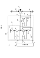
- 2A to 2C are diagrams illustrating details of a switching driver according to a first embodiment.
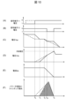
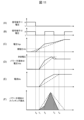
- 5A to 5F are diagrams illustrating examples of waveforms of each signal at the time of turn-off in the first embodiment.
- 5A to 5F are diagrams illustrating examples of waveforms of signals at turn-on in the first embodiment.
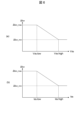
- FIG. 1 is a diagram showing a configuration for detecting the state of a power semiconductor in a switching driver; 1A shows the relationship between the time width at turn-off and the drain-source voltage, and
- FIG. 1B shows the relationship between the time width at turn-off and the drain-source current.
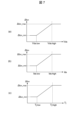
- FIG. 6A, 6B, and 6C are diagrams illustrating a method for setting the time width at turn-on.
- FIG. 13 is a diagram illustrating a modified example of the first embodiment.
- 11A and 11B are diagrams illustrating a switching driver according to a second embodiment.
- 13A, 13B, 13C, 13D, 13E, and 13F are diagrams illustrating example waveforms of signals at turn-off in the second embodiment.
- 13A, 13B, 13C, 13D, 13E, and 13F are diagrams illustrating examples of waveforms of signals at turn-on in the second embodiment.
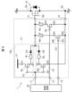
- FIG. 13 is a diagram showing a switching driver according to a third embodiment.
- Fig. 1 is a diagram showing an application example of the switching drive device of this embodiment, and is a diagram showing a part of the configuration of a power conversion device.
- the power conversion device drives, for example, an electric motor mounted on an electric vehicle.
- the electric motor has a three-phase coil, and the power conversion device is provided with a three-phase switching arm for applying a predetermined current pattern to the three-phase coil.
- Fig. 1 shows a three-phase switching arm 500U, which is one phase of a three-phase switching arm 500U, 500V, 500W provided in the power conversion device.
- the three-phase switching arm 500U is provided with an upper arm power semiconductor 42 and a lower arm power semiconductor 41.
- semiconductor elements such as IGBTs, Si-MOSFETs, and GaN-MOSFETs are used. Note that FIG. 1 shows a case where MOSFETs are used for the power semiconductors 41 and 42.
- the power semiconductors 41 and 42 are provided with a high-voltage side terminal for the main circuit (collector terminal for an IGBT, drain terminal for a MOSFET), a low-voltage side terminal for the main circuit (emitter terminal for an IGBT, source terminal for a MOSFET), and a control terminal (gate terminal). Note that multiple power semiconductors may be connected in parallel depending on the desired output current value.
- the positive wiring 52 on the upper arm side is connected to the positive terminal of a DC voltage source such as a battery (not shown).
- the negative wiring 51 on the lower arm side is connected to the negative terminal of the DC voltage source.
- the positive wiring 52 is connected to the high-voltage side terminal (drain terminal) for the main circuit of the power semiconductor 42.
- the low-voltage side terminal (source terminal) for the main circuit of the power semiconductor 42 is connected to the output terminal 53 of the three-phase switching arm 500U and the high-voltage side terminal (drain terminal) for the main circuit of the power semiconductor 41.
- the low-voltage side terminal (source terminal) for the main circuit of the power semiconductor 41 is connected to the negative wiring 51.
- the output terminal 53 is connected to a load such as an electric motor.
- the gate terminal Gp and source terminal Sp of the power semiconductor 41 are connected to the gate terminal 13 and source terminal 14, respectively, of the gate driver 10 that supplies driving power to the power semiconductor 41.
- the gate terminal Gp and source terminal Sp of the power semiconductor 42 are connected to the gate terminal 13 and source terminal 14, respectively, of the gate driver 20 that supplies driving power to the power semiconductor 42.
- the gate drive devices 10, 20 are connected to a control circuit 30.
- the control circuit 30 is composed of, for example, a microcomputer.
- the control circuit 30 outputs control commands for each of the gate drive devices 10, 20 based on drive commands input from a higher-level control device (not shown), and individually controls the on/off of each of the power semiconductors 41, 42. As a result, an AC voltage is output to a load such as an electric motor via the output terminal 53.
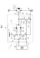
- FIG. 2 is a diagram for explaining the details of a switching drive device.
- the basic configuration of a switching drive device is composed of either one of gate drive devices 10 or 20 and a control circuit 30, and the example shown in FIG. 2 shows a switching drive device 1 composed of gate drive device 10 and control circuit 30.
- a switching drive device composed of gate drive device 20 and control circuit 30 has the same configuration as the switching drive device 1 shown in FIG. 2 and operates in the same way. The following explanation takes switching drive device 1 as an example.
- FIG. 2 shows a power semiconductor 41 and a switching driver 1 corresponding to the power semiconductor 41, and shows details of the gate driver 10.
- the gate driver 20 in FIG. 1 has a similar configuration to the gate driver 10.
- the gate driver 10 comprises a first charging circuit C1 having a switching element M1, a first discharging circuit C2 having a switching element M2, and a second discharging circuit C3 having a switching element M3.
- the power semiconductor 41 and switching elements M2 and M3 are N-type MOSFETs
- the switching element M1 is a P-type MOSFET.
- the first charging circuit C1 includes a positive power supply V1, a switching element M1, an on-gate resistor R1, and a backflow prevention diode Di1.
- the source terminal S1 of the switching element M1 is connected to the positive power supply V1.
- the gate terminal G1 of the switching element M1 is connected to a signal terminal 11 of the gate driver 10.
- the drain terminal D1 of the switching element M1 is connected to one end of the on-gate resistor R1.
- the other end of the on-gate resistor R1 is connected to the anode of the backflow prevention diode Di1.
- the first discharge circuit C2 includes a switching element M2, an off-gate resistor R2, and a backflow prevention diode Di2.
- the source terminal S2 of the switching element M2 is connected to the source terminal 14 of the gate drive device 10.
- the gate terminal G2 of the switching element M2 is connected to the signal terminal 11 of the gate drive device 10.
- the drain terminal D2 of the switching element M2 is connected to one end of the off-gate resistor R2.
- the other end of the off-gate resistor R2 is connected to the cathode of the backflow prevention diode Di2.
- the second discharge circuit C3 includes a switching element M3 and a charge/discharge gate resistor R3.
- One end of the charge/discharge gate resistor R3 is connected to the gate terminal 13 of the gate drive device 10.
- the other end of the charge/discharge gate resistor R3 is connected to the drain terminal D3 of the switching element M3.
- the source terminal S3 of the switching element M3 is connected to the source terminal 14 of the gate drive device 10.
- the gate terminal G3 of the switching element M3 is connected to the signal terminal 12 of the gate drive device 10.
- the cathode of the reverse current prevention diode Di1 is connected to the anode of the reverse current prevention diode Di2, and is also connected to the gate terminal 13 of the gate driver 10 and one end of the charge/discharge gate resistor R3.
- the first discharge circuit C2 and the second discharge circuit C3 are connected in parallel to the gate terminal 13. Note that the reverse current prevention diodes Di1 and Di2 may be omitted.
- the signal terminals 11, 12 of the gate driver 10 are connected to the control circuit 30.
- the gate terminal 13 of the gate driver 10 is connected to the gate terminal Gp of the power semiconductor 41.
- the source terminal 14 of the gate driver 10 is connected to the source terminal Sp of the power semiconductor 41. Note that, although the signal terminals 11, 12 are connected to a common control circuit 30 in the example shown in FIG. 2, each of the signal terminals 11, 12 may be individually connected to two independently provided control circuits.
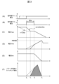
- FIG. 3 is a diagram showing an example of the waveforms of each signal when the power semiconductor 41 is turned off.
- Waveform (A) shows the voltage waveform of the signal terminal 11.
- Waveform (B) shows the voltage waveform of the signal terminal 12.
- Waveform (C) shows the voltage between the gate and source (GpSp) of the power semiconductor 41 (hereinafter referred to as the gate-source voltage Vgs).
- waveform (D) shows the voltage between the drain and source (DpSp) of the power semiconductor 41 (hereinafter referred to as the drain-source voltage Vds).
- Waveform (E) shows the current flowing between the drain and source (DpSp) of the power semiconductor 41 (hereinafter referred to as the drain-source current Ids).
- Waveform (F) shows the waveform of the switching loss of the power semiconductor 41. Note that the waveforms shown by the dashed lines in FIG. 3 show signal waveforms in the case of a configuration in which the second discharge circuit C3 is deleted from the circuit diagram shown in FIG. 2 (hereinafter referred to as the conventional configuration).
- a control command to turn off power semiconductor 41 is input from control circuit 30 to signal terminal 11 of gate driver 10. That is, the voltage of signal terminal 11 is switched from L level to H level.
- this signal is input to gate terminals G1, G2 of switching elements M1, M2, switching element M1, which is a P-type MOSFET, switches from on to off, and switching element M2, which is an N-type MOSFET, switches from off to on.
- waveform (B) at time t0, a control command to switch switching element M3 from OFF to ON is input to signal terminal 12. That is, the voltage of signal terminal 12 is switched from L level to H level.
- switching element M3 which is an N-type MOSFET, switches from OFF to ON. Note that the timing at which the control command to switch ON is input to signal terminal 12 may be later than time t0.
- switching element M2 When switching element M2 is turned on (switching element M1 is turned off) at time t0, the gate-source capacitance of power semiconductor 41 starts to be discharged from the gate terminal Gp of power semiconductor 41 in FIG. 2 via backflow prevention diode Di2, off gate resistor R2, and switching element M2. Also, when switching element M3 is turned on at time t0, the gate-source capacitance of power semiconductor 41 starts to be discharged from the gate terminal Gp of power semiconductor 41 via charge/discharge gate resistor R3 and switching element M3. As a result, as shown by the solid line in waveform (C), the gate-source voltage Vgs of power semiconductor 41 starts to decrease.
- the drain-source voltage Vds of the power semiconductor 41 starts to increase, as shown by the solid line in waveform (D).
- the dashed line in waveform (C) if the gate capacitance of the power semiconductor 41 is C, the discharge time constant ⁇ 1 of the drain-source voltage Vds of the power semiconductor 41 is CR2.
- the switching element M3 is also turned on at time t0, so the discharge time constant ⁇ 2 of the drain-source voltage Vds of the power semiconductor 41 is C(R2//R3).
- R2//R3 represents the combined resistance of the parallel-connected resistors R2 and R3. Therefore, while the switching element M3 is on (t1 to t2), the discharge speed of the gate-source voltage Vgs of the power semiconductor 41 is accelerated, and the drain-source voltage Vds increases rapidly.
- the current (drain-source current Ids) flowing between the drain and source of the power semiconductor 41 starts to decrease as shown in waveform (E).
- a control command to turn off the switching element M3 is input from the control circuit 30 to the signal terminal 12. That is, the voltage of the signal terminal 12 is switched from the H level to the L level.
- the timing at which the control command to turn off is input to the signal terminal 12 may be later than time t2.
- the discharge time constant of the gate-source voltage Vgs of the power semiconductor 41 is CR2, which is the same as in the conventional configuration. Therefore, the surge voltage between the drain and source of the power semiconductor 41 related to the discharge time constant that occurs after time t2 is the same as in the conventional configuration.
- the amount of switching loss of the power semiconductor 41 is represented by the integrated total value of the drain-source voltage Vds of the power semiconductor 41 and the drain-source current Ids of the power semiconductor 41.
- the off-gate resistance R2 is set large to suppress the drain-source voltage Vds of the power semiconductor 41 to an allowable voltage or less, and switching loss occurs from time t0 to time t3.
- the discharge speed is increased by turning on the switching element M3 at time t0, so that loss occurs in a shorter period from time t1 to time t3 as shown in the waveform (F).
- the period in which switching loss occurs is shorter than in the case of the conventional configuration (dashed line), so the amount of loss, which is the time integral value of loss, is also smaller than in the case of the conventional configuration. That is, in the first embodiment, the amount of switching loss at turn-off can be reduced compared to the case of the conventional configuration.
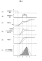
- (Explanation of turn-on operation) 4 is a diagram showing an example of the waveforms of each signal when the power semiconductor 41 is turned on.
- Waveform (A) shows the voltage waveform of the signal terminal 11.
- Waveform (B) shows the voltage waveform of the signal terminal 12.
- Waveform (C) shows the gate-source voltage Vgs of the power semiconductor 41.
- Waveform (D) shows the drain-source voltage Vds of the power semiconductor 42 on the upper arm side shown in FIG. 1.
- Waveform (E) shows the drain-source current Ids of the power semiconductor 41.
- Waveform (F) shows the switching loss of the power semiconductor 41.
- the waveforms shown by dashed lines show signal waveforms in the case of a conventional configuration.
- a control command to turn on the power semiconductor 41 is input from the control circuit 30 to the signal terminal 11 of the gate driver 10. That is, the voltage of the signal terminal 11 is switched from H level to L level.
- this signal is input to the gate terminals G1 and G2 of the switching elements M1 and M2, the switching element M1 switches from off to on, and the switching element M2 switches from on to off.
- the switching element M1 is turned on, the gate-source capacitance of the power semiconductor 41 in FIG. 2 is charged by the charging current that flows through the positive power supply V1, the switching element M1, the backflow prevention diode Di1, and the on-gate resistor R1.
- the gate-source voltage Vgs of the power semiconductor 41 begins to increase as shown by the solid line in waveform (C).
- the drain-source voltage Vds of the power semiconductor 42 on the upper arm side in FIG. 1 begins to increase, and the drain-source current Ids of the power semiconductor 41 begins to increase.
- the drain-source voltage Vds of the power semiconductor 41 decreases, and conversely, the drain-source voltage Vds of the power semiconductor 42 on the upper arm side, which is in the off state, increases.
- a control command to turn on switching element M3 is input from control circuit 30 to signal terminal 12. That is, the voltage of signal terminal 12 is switched from L level to H level. Note that the timing at which the ON control command is input to signal terminal 12 may be earlier than time t2.
- the switching element M3 turns on, and the gate-source capacitance of the power semiconductor 41 is discharged from the gate terminal Gp of the power semiconductor 41 via the charge-discharge gate resistor R3 and the switching element M3.
- the gate-source voltage Vgs of the power semiconductor 41 converges to a voltage value determined by the ratio of the charge-discharge gate resistor R3 of the second discharge circuit C3 to the on-gate resistor R1 of the first charge circuit C1.
- the gate-source voltage Vgs of the power semiconductor 41 is kept constant from time t2 to time t3. Therefore, the change in the drain-source current Ids of the power semiconductor 41 becomes gradual, and the increase in the drain-source voltage Vds of the power semiconductor 42 on the upper arm side becomes gradual and is suppressed.
- a control command to turn off switching element M3 is input from control circuit 30 to signal terminal 12. That is, the voltage of signal terminal 12 is switched from H level to L level. Note that the timing at which the OFF control command is input to signal terminal 12 may be later than time t3. As shown by the solid line in waveform (F), switching loss in power semiconductor 41 occurs from time t1 to time t4.
- the on-gate resistance R1 is set large in order to suppress the drain-source voltage Vds of the power semiconductor 42 on the upper arm side to below the allowable voltage.
- the charging speed is slowed down by turning on the switching element M3, and the drain-source voltage Vds of the power semiconductor 42 is suppressed to below the allowable voltage. Therefore, it is possible to set the on-gate resistance R1 smaller than in the conventional configuration, and the charging speed during the period when the switching element M3 is off can be made faster than before.
- the waveform (F) the period during which losses occur is shorter than in the conventional configuration (dashed line). That is, in the first embodiment, the amount of switching loss at turn-on can be reduced compared to the conventional configuration.
- Control command generating method in control circuit 30 Next, a method of generating a control command in the control circuit 30 will be described.
- the control command from the control circuit 30 described above is preferably generated according to the state of the power semiconductor 41.
- Fig. 5 shows a circuit configuration related to the switching driver 1, similar to Fig. 2, and includes a means for detecting the state of the power semiconductor 41.
- the means for detecting the state of the power semiconductor 41 include an element current detection unit 61 that detects the drain-source current Ids of the power semiconductor 41, an element voltage detection unit 62 that detects the drain-source voltage Vds of the power semiconductor 41, and an element temperature detection unit 63 that detects the temperature Tj of the power semiconductor 41.
- the control circuit 30 receives a drive command S from a higher-level control device and state detection information (Ids, Vds, Tj) of each detection unit 61 to 63.
- the control circuit 30 sends control commands to each of the signal terminals 11 and 12 of the gate driver 10 based on only the drive command S, or on both the drive command S and the state detection information (Ids, Vds, Tj).
- the state detection information for the power semiconductor 41 can be any information other than the above, such as the rising edge of the rate of change of the drain-source voltage Vds, or the falling edge of the rate of change of the drain-source voltage Vds and the drain-source current Ids. In this way, the control circuit 30 can more appropriately control the switching operation of the power semiconductor 41 by generating a control command according to the detected state of the power semiconductor 41.
- control circuit 30 instead of the control circuit 30, a control circuit 30A that outputs a control command to the signal terminal 11 and a control circuit 30B that outputs a control command to the signal terminal 12 may be provided separately.
- the drive command S from the higher level and the state detection information (Ids, Vds, Tj) of the power semiconductor 41 are input separately to each of the control circuits 30A and 30B.
- the time width of the H level of the control command input to the signal terminal 12 of the gate driver 10 in FIG. 2, i.e., the H level of the voltage of the signal terminal 12 shown in the waveform (B) in FIG. 3 and FIG. 4, is ⁇ t on.
- the time width ⁇ t on may be set based on the drain-source voltage Vds of the power semiconductor 41 detected by the element voltage detection unit 62 in FIG. 5, or based on the drain-source current Ids detected by the element current detection unit 61. In that case, both the detection values of the element voltage detection unit 62 and the element current detection unit 61 may be used, or only one of them may be used.
- FIG. 6(a) shows a case where the time width ⁇ t on at the time of turning off is set based on the drain-source voltage Vds.
- the larger the detection value of the element voltage detection unit 62 the smaller the time width ⁇ t on is set, and the smaller the detection value, the larger the time width ⁇ t on is set.
- a maximum value ( ⁇ t on_max) or a minimum value ( ⁇ t on_min) may be set for the time width ⁇ t on.
- the value of the time width ⁇ t on does not have to be changed linearly, and a discrete value may be used.
- the reason for setting in this way is that the smaller the drain-source voltage Vds of the power semiconductor 41, the larger the voltage difference to the allowable voltage, and the faster the switching speed can be achieved.
- FIG. 6(b) shows a case where the time width ⁇ t on at turn-off is set based on the drain-source current Ids.
- the larger the detection value of the element current detection unit 61 the smaller the time width ⁇ t on is set, and the smaller the detection value of the element current detection unit 61, the larger the time width ⁇ t on is set.
- a maximum value ( ⁇ t on_max) or a minimum value ( ⁇ t on_min) may be set for the time width ⁇ t on.
- the value of the time width ⁇ t on does not have to change linearly, and a discrete value may be used.
- the reason for setting it in this way is that the smaller the drain-source current Ids of the power semiconductor 41, the larger the voltage difference up to the allowable voltage, and the faster the switching speed can be.
- the time width ⁇ t on as shown in FIG. 6(b) high-speed switching can be achieved over a wider range according to the drain-source current Ids of the power semiconductor 41, and switching losses are reduced.
- the fall time of the time width ⁇ t on of the voltage signal of the signal terminal 12 may be, for example, the end time of turning on the power semiconductor 41, or a value obtained by adding or subtracting any time from the end time of turning on.
- the rise time of the time width ⁇ t on is set to a value obtained by subtracting the time width ⁇ t on from the fall time.
- FIG. 7(a) shows a case where the time width ⁇ t on at turn-on is set based on the drain-source voltage Vds detected by the element voltage detection unit 62.
- the larger the detection value of the element voltage detection unit 62 the larger the time width ⁇ t on is set, and the smaller the detection value, the smaller the time width ⁇ t on is set.
- a maximum value ( ⁇ t on_max) or a minimum value ( ⁇ t on_min) may be set for the time width ⁇ t on.
- the value of the time width ⁇ t on does not have to change linearly, and a discrete value may be used.
- the reason for setting it in this way is that the smaller the drain-source voltage Vds of the power semiconductor 41, the larger the voltage difference to the allowable voltage becomes, and thus by performing such a turn-on operation, the switching speed can be made faster.
- the time width ⁇ t on as in FIG. 7(a) high-speed switching can be realized over a wider range according to the drain-source voltage Vds of the power semiconductor 41, and switching losses are reduced.
- FIG. 7(b) shows a case where the time width ⁇ t on at turn-on is set based on the drain-source current Ids detected by the element current detection unit 61.
- the larger the detection value of the element current detection unit 61 the larger the time width ⁇ t on is set, and the smaller the detection value of the element current detection unit 61, the smaller the time width ⁇ t on is set.
- a maximum value ( ⁇ t on_max) or a minimum value ( ⁇ t on_min) may be set for the time width ⁇ t on.
- the value of the time width ⁇ t on does not have to change linearly, and a discrete value may be used.
- the reason for setting it in this way is that the smaller the drain-source current Ids of the power semiconductor 41, the larger the voltage difference to the allowable voltage becomes, and by performing such a turn-on operation, the switching speed can be made faster.
- the time width ⁇ t on as in FIG. 7(b) high-speed switching can be achieved over a wider range according to the drain-source current Ids of the power semiconductor 41, and switching losses are reduced.
- FIG. 7(c) shows a case where the time width ⁇ t on at the time of turning on is set based on the temperature Tj of the power semiconductor 41 detected by the element temperature detection unit 63.
- the higher the temperature Tj the larger the time width ⁇ t on is set, and the smaller the temperature Tj, the smaller the time width ⁇ t on is set.
- a maximum value ( ⁇ t on_max) or a minimum value ( ⁇ t on_min) may be set for the time width ⁇ t on.
- the value of the time width ⁇ t on does not have to change linearly, and a discrete value may be used.
- the reason for setting it in this way is that the lower the temperature Tj of the power semiconductor 41, the larger the voltage difference up to the allowable voltage becomes, and by performing such a turn-on operation, the switching speed can be made faster.
- the time width ⁇ t on as in FIG. 7(c) high-speed switching can be achieved over a wider range according to the temperature Tj of the power semiconductor 41, and switching losses are reduced.
- FIG. 8 is a diagram showing a modification of the first embodiment described above.
- the second discharge circuit C3 is configured with two discharge circuits connected in parallel.
- One of the parallel-connected discharge circuits includes a charge/discharge gate resistor 3R and a switching element M3, and the other includes a charge/discharge gate resistor 5R and a switching element M5.
- the charge/discharge gate resistors 3R and 5R are variable resistors, but they do not have to be variable resistors. Note that the number of discharge circuits connected in parallel in the second discharge circuit C3 may be three or more.
- the values of the charge/discharge gate resistors 3R and 5R may be determined according to a control command from the control circuit 30, or may be determined using the detection values of the element current detector 61, element voltage detector 62, and element temperature detector 63 shown in FIG. 5. In the case of the configuration in FIG. 8, for example, when turning off, all of the switching elements M2, M3, and M5 can be turned on to further increase the speed. Note that, in the case of the second discharge circuit C3 shown in FIG. 2, by making the charge/discharge gate resistor R3 a variable resistor, for example, by controlling the value of the variable resistor according to the value of the element temperature Tj, more appropriate charge/discharge control can be performed.
- Second Embodiment Fig. 9 is a diagram for explaining a switching driver 1 according to a second embodiment of the present invention.
- the switching driver 1 shown in Fig. 9 includes a control circuit 30 and a gate driver 10A that sends driving power to a power semiconductor 41.
- the switching driver for the power semiconductor 42 on the upper arm side also includes a gate driver having a similar configuration to the gate driver 10A.
- the gate driver 10A includes a first charging circuit C1 having a switching element M1, a first discharging circuit C2 having a switching element M2, and a second charging circuit C4 having a switching element M4.
- a first charging circuit C1 having a switching element M1 having a switching element M1
- a first discharging circuit C2 having a switching element M2 having a switching element M2
- a second charging circuit C4 having a switching element M4 having a switching element M4.
- the first charging circuit C1 and the first discharging circuit C2 of the gate driving device 10A have the same configuration as the first charging circuit C1 and the first discharging circuit C2 of the gate driving device 10 shown in FIG. 2.
- the second charging circuit C4 includes a switching element M4 and a charge/discharge gate resistor R4.
- the source terminal S4 of the switching element M4 is connected to the positive power supply V2.
- the gate terminal G4 of the switching element M4 is connected to the signal terminal 12 of the gate driving device 10A.
- the drain terminal D4 of the switching element M4 is connected to one end of the charge/discharge gate resistor R4.
- the other end of the charge/discharge gate resistor R4 is connected to the gate terminal 13 of the gate driving device 10A.
- the cathode of the reverse current prevention diode Di1 is connected to the anode of the reverse current prevention diode Di2, and is also connected to the gate terminal 13 of the gate driver 10A and the other end of the charge/discharge gate resistor R4.
- the first charging circuit C1 and the second charging circuit C4 are connected in parallel to the gate terminal 13. Note that the reverse current prevention diodes Di1 and Di2 may be omitted.
- the signal terminals 11 and 12 of the gate driver 10A are connected to the control circuit 30.
- the gate terminal 13 of the gate driver 10A is connected to the gate terminal Gp of the power semiconductor 41.
- the source terminal 14 of the gate driver 10A is connected to the source terminal Sp of the power semiconductor 41.
- the signal terminals 11 and 12 are connected to a common control circuit 30, but the signal terminals 11 and 12 may be individually connected to two control circuits that are provided independently.
- the potentials of the positive power supplies V1 and V2 may be different, but are generally set to be equal, and in this embodiment, an example in which they are set to the same potential will be described.
- Fig. 10 is a diagram showing an example of the waveforms of each signal when the power semiconductor 41 is turned off.
- Waveform (A) shows the voltage waveform of the signal terminal 11.
- Waveform (B) shows the voltage waveform of the signal terminal 12.
- Waveform (C) shows the gate-source voltage Vgs of the power semiconductor 41.
- Waveform (D) shows the drain-source voltage Vds of the power semiconductor 41.
- Waveform (E) shows the drain-source current Ids of the power semiconductor 41.
- Waveform (F) shows the waveform of the switching loss of the power semiconductor 41. Note that the waveforms shown by dashed lines in Fig. 10 show signal waveforms in the case of a conventional configuration in which the second charging circuit C4 is deleted from the circuit diagram shown in Fig. 9.
- a control command to turn off power semiconductor 41 is input from control circuit 30 to signal terminal 11 of gate driver 10. That is, the voltage of signal terminal 11 is switched from L level to H level.
- this signal is input to gate terminals G1, G2 of switching elements M1, M2, switching element M1, which is a P-type MOSFET, switches from on to off, and switching element M2, which is an N-type MOSFET, switches from off to on.
- switching element M2 When switching element M2 is turned on (switching element M1 is turned off) at time t0, the gate-source capacitance of power semiconductor 41 starts to discharge from the gate terminal Gp of power semiconductor 41 via backflow prevention diode Di2, off-gate resistor R2, and switching element M2. As a result, as shown by the solid line in waveform (C), the gate-source voltage Vgs of power semiconductor 41 starts to decrease.
- the value of the off-gate resistor R2 is set large in order to suppress the drain-source voltage Vds of the power semiconductor 41 below the allowable voltage.
- the value of the off-gate resistor R2 of the first discharge circuit C2 in the second embodiment is set smaller than that in the case of the conventional configuration.
- the value of the off-gate resistor R2 is set so that the discharge time constant of the gate-source voltage Vgs from time t0 to time t1 is the same as the time constant ⁇ 2 shown in FIG. 3. Therefore, the slope of the solid line of the gate-source voltage Vgs from time t0 to time t1 in FIG. 10 is the same as the slope of the solid line from time t0 to t1 in the waveform (C) in FIG. 3.
- the drain-source voltage Vds of the power semiconductor 41 begins to increase, as shown by the solid line in waveform (D).
- the mirror period for the gate-source voltage Vgs of the power semiconductor 41 ends at time t2, as shown by the solid line in waveform (C), the drain-source current Ids of the power semiconductor 41 begins to decrease, as shown in waveform (E).
- a control command to turn on switching element M4 is input from control circuit 30 to signal terminal 12. That is, the voltage of signal terminal 12 is switched from H level to L level. Note that the timing at which the ON control command is input to signal terminal 12 (time t21) may be later than time t2.
- switching element M4 When switching element M4 is turned on at time t21, a charging current flows through the positive power supply V2, switching element M4, and charge/discharge gate resistance R4. As a result, when switching element M4 is on, the gate-to-source voltage Vgs of power semiconductor 41 converges to a voltage value determined by the ratio of charge/discharge gate resistance R4 of the second charging circuit C4 to the off-gate resistance R2 of the first discharging circuit C2. In this way, by turning on switching element M4 while discharging is being performed in the first discharging circuit C2, the discharge rate is slowed down, and the drain-to-source voltage Vds of power semiconductor 41 is suppressed to below the allowable voltage.
- the timing when an OFF control command is input to the signal terminal 12, i.e., the timing when the L level switches to the H level, t3, may be simultaneous with the time t3 when the drain-source current Ids becomes zero, or may be later than time t3.
- (Explanation of turn-on operation) 11 is a diagram showing an example of the waveforms of each signal when the power semiconductor 41 is turned on.
- Waveform (A) shows the voltage waveform of the signal terminal 11.
- Waveform (B) shows the voltage waveform of the signal terminal 12.
- Waveform (C) shows the gate-source voltage Vgs of the power semiconductor 41.
- Waveform (D) shows the drain-source voltage Vds of the power semiconductor 42 on the upper arm side shown in FIG. 1.
- Waveform (E) shows the drain-source current Ids of the power semiconductor 41.
- Waveform (F) shows the switching loss of the power semiconductor 41.
- the waveforms shown by dashed lines show signal waveforms in the case of a conventional configuration in which the second charging circuit C4 is deleted from the circuit diagram shown in FIG. 9.
- a control command to turn on the power semiconductor 41 is input from the control circuit 30 to the signal terminal 11 of the gate driver 10. That is, the voltage of the signal terminal 11 is switched from H level to L level.
- this signal is input to the gate terminals G1, G2 of the switching elements M1, M2, the switching element M1 switches from off to on, and the switching element M2 switches from on to off.
- the switching element M1 is turned on (switching element M2 is off) at time t0, a charging current flows via the positive power supply V1, the switching element M1, the reverse current prevention diode Di1, and the on-gate resistor R1.
- a control command to switch switching element M4 from OFF to ON is input from control circuit 30 to signal terminal 12. That is, the voltage of signal terminal 12 is switched from H level to L level.
- switching element M4 is turned ON at time t0, a charging current flows via positive power supply V2, switching element M4, and charge/discharge gate resistor R4. Note that the timing at which the ON control command is input to signal terminal 12 may be later than time t0.
- the charging time constant ⁇ 3 of the drain-source voltage Vds of the power semiconductor 41 is CR1, assuming that the gate capacitance of the power semiconductor 41 is C.
- the charging time constant ⁇ 4 of the drain-source voltage Vds of the power semiconductor 41 is C(R1//R4). Note that R1//R4 represents the combined resistance of the parallel-connected resistors R1 and R4. Therefore, while the switching element M4 is on, the charging speed of the gate-source voltage Vds of the power semiconductor 41 is increased, and the drain-source voltage Vds increases more rapidly than in the conventional case.
- a control command to turn off switching element M4 is input from control circuit 30 to signal terminal 12. That is, the voltage of signal terminal 12 is switched from L level to H level.
- the timing at which the OFF control command is input to signal terminal 12 may be later than time t2.
- the charging time constant of gate-to-source voltage Vgs of power semiconductor 41 is CR1, the same as in the conventional configuration. Therefore, the drain-to-source surge voltage of power semiconductor 41 related to the charging time constant that occurs after time t2 is the same as in the conventional configuration.
- the switching loss of the power semiconductor 41 occurs between time t1 and time t4, and the loss period can be made shorter than in the case of the conventional configuration (dashed line) in which the on-gate resistance R1 is increased to suppress the drain-source voltage Vds of the power semiconductor 42 of the paired arm.
- the amount of switching loss at turn-on can be reduced compared to the case of the conventional configuration.
- a control command to turn on switching element M4 may be input from control circuit 30 to signal terminal 12, and high-speed switching may be performed.
- switching element M4 is on, as shown in waveform (C), the gate-source voltage Vgs rises at high speed, accelerating the turn-on operation and further reducing the switching loss of power semiconductor 41.
- the configuration including the element current detection unit 61, element voltage detection unit 62, and element temperature detection unit 63 shown in FIG. 5 can also be applied.
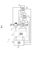
- FIG. 12 is a diagram showing a switching driver 1 according to a third embodiment.
- the gate driver 10 shown in FIG. 2 is a voltage-driven gate driver, but the gate driver 10B shown in FIG. 12 shows an example in which the voltage-driven type is changed to a constant-current-driven type.
- the switching elements M1, M2, and M3 are replaced with constant-current-driven switching elements. Note that, although an operational amplifier is used in FIG. 12, the system does not have to be a system using an operational amplifier.
- a control command is input from the control circuit 30 to the positive input terminal of each operational amplifier via signal terminals 11, 12, and 15 of the gate driver 10B.
- switching elements M1, M2, and M3 can be configured as shown in FIG. 12, and switching element M1 can be configured as shown in FIG. 2.
- a voltage drive the circuit configuration is simple, but the amount of current varies depending on the load.
- a constant current drive is easy to control because the current is constant, but the circuit configuration is somewhat more complicated than when it is a voltage drive.
- the switching drive device 1 supplies a drive voltage or drive current to the gate terminal Gp of the power semiconductor 41.
- the switching drive device 1 includes a first circuit (first charging circuit C1) having a turn-on resistor R1 and a first switching element M1, and charging the gate terminal Gp when the power semiconductor 41 is turned on.
- the second circuit (first discharging circuit C2) has a turn-off resistor R2 and a second switching element M2, and discharges the gate terminal Gp when the power semiconductor 41 is turned off.
- the third circuit (second discharging circuit C3 or second charging circuit C4) is connected to the gate terminal Gp and has a gate resistor (charge/discharge gate resistor R3 or R4) and a third switching element M3 or M4 to discharge or charge the gate terminal Gp.
- the third circuit (second discharging circuit C3 or second charging circuit C4) has a gate resistor (charge/discharge gate resistor R3 or R4) and a third switching element M3 or M4, and a control device (control circuit 30) that controls the on/off of the first to third switching elements M1 to M4.
- the control circuit 30 controls charging by the first circuit (first charging circuit C1) and charging or discharging by the third circuit (second discharging circuit C3 or second charging circuit C4) to execute the first turn-on operation mode from time t0 to t2 in FIG. 4 or FIG. 11, and then executes the second turn-on operation mode from time t2 to t3 in FIG. 4 or from time t2 to t3 in FIG. 11, which is slower than the first turn-on operation mode.
- the discharge by the second circuit (first discharge circuit C2) and the discharge or charge by the third circuit (second discharge circuit C3 or second charge circuit C4) are controlled to execute the first turn-off operation mode from time t0 to t2 in FIG. 3 or from time t0 to t21 in FIG. 10, and then the second turn-off operation mode, which is slower than the first turn-off operation mode, from time t2 to t3 in FIG. 3 or from time t21 to t3 in FIG. 10, is executed.
- the first and second turn-off operation modes in this way it is possible to shorten the period during which switching losses occur in the power semiconductor 41 while suppressing the surge voltage at the time of turn-off. As a result, the amount of switching loss at the time of turn-off can be reduced.
- the switching drive device 1 can suppress surges and reduce switching losses at turn-on and turn-off while minimizing cost increases by simply adding a third circuit (second discharge circuit C3 or second charge circuit C4) to the first circuit (first charge circuit C1) and second circuit (first discharge circuit C2).
- the third circuit is a second discharge circuit C3 provided in parallel with the first discharge circuit C2 (second circuit).
- charging is performed by the first charging circuit C1 (first circuit)
- second turn-on operation mode from time t2 to t3 charging is performed by the first charging circuit C1
- discharging is performed by the second discharging circuit C3.
- discharging is performed by the first discharging circuit C2 and the second discharging circuit C3
- discharging is performed by the first discharging circuit C2.
- discharging is performed by the first discharging circuit C2 and the second discharging circuit C3, so that the discharge time constant ⁇ 2 of the drain-source voltage Vds of the power semiconductor 41 becomes C(R2//R3), and the discharge speed of the gate-source voltage Vds of the power semiconductor 41 is increased.
- the period during which switching loss occurs is shorter than before, and the amount of switching loss at turn-off can be reduced.
- the third circuit is a second charging circuit C4 that is provided in parallel with the first charging circuit C1 (first circuit).
- charging is performed by the first charging circuit C1 and by the second charging circuit C4, and in the second turn-on operation mode from time t2 to t3, charging is performed by the first charging circuit C1.
- discharging is performed by the first discharging circuit C2
- second turn-off operation mode from time t21 to t3
- discharging is performed by the first discharging circuit C2 and charging is performed by the second charging circuit C4.
- the discharge speed of the gate-source voltage Vds of the power semiconductor 41 is increased, the period during which switching losses occur is shorter than in the past, and the amount of switching loss at turn-on can be reduced.
- the discharge speed in the second turn-off operation mode shown in FIG. 10 is slowed by turning on the switching element M4 while discharging in the first discharge circuit C2, so it is possible to set the off-gate resistor R2 smaller than in the past. As a result, the discharge speed in the first turn-off operation mode is increased, the period during which switching losses occur is shorter than in the past, and the amount of switching loss at turn-off can be reduced.
- a detection unit (element current detection unit 61, element voltage detection unit 62, element temperature detection unit 63) is further provided that detects at least one of the voltage Vds, current Ids, and temperature Tj of the power semiconductor 41, and the control circuit 30 controls the on/off of the third switching element M3 based on the detection information (voltage Vds, current Ids, and temperature Tj) of the detection unit. In this way, by controlling the on/off of the third switching element M3 according to the detected state of the power semiconductor 41, the switching operation of the power semiconductor 41 can be more appropriately controlled.
- the discharge period (time duration ⁇ t on ) by the third circuit (second discharge circuit C3) in the first turn-off operation mode from time t0 to t2 in FIG. 3 is set to be longer as the input voltage (drain-source voltage Vds) of the power semiconductor 41 or the drain-source current Ids flowing through the power semiconductor 41 becomes lower, as shown in FIGS. 6(a) and 6(b).
- the discharge period (time duration ⁇ t on ) by the third circuit (second discharge circuit C3) in the second turn-on operation mode from time t2 to t3 in FIG. 4 is set to be longer as the input voltage Vds of the power semiconductor 41, the drain-source current Ids flowing through the power semiconductor 41, or the device temperature Tj of the power semiconductor 41 increases, as shown in FIG. 7.
- 1...Switching driver 10, 10A, 10B, 20...Gate driver, 30...Control circuit, 41, 42...Power semiconductor, 51...Negative wiring, 52...Positive wiring, 53...Output terminal, 61...Element current detector, 62...Element voltage detector, 63...Element temperature detector, C1...First charging circuit, C2...First discharging circuit, C3...Second discharging circuit, Di1, Di2...Backflow prevention diode, M1, M2, M3, M4, M5...Switching element, R1...On gate resistor, R2...Off gate resistor, R3, R4, R5...Charge/discharge gate resistor, V1, V2...Positive power supply, ⁇ t on...Time width
Landscapes
- Engineering & Computer Science (AREA)
- Power Engineering (AREA)
- Power Conversion In General (AREA)
Abstract
Description
図1は、本実施の形態のスイッチング駆動装置の適用例を示す図であり、電力変換装置の構成の一部を示す図である。電力変換装置は、例えば、電動車両に搭載された電動モータを駆動する。電動モータは3相コイルを有し、電力変換装置には、3相コイルに所定の通電パターンを印加するための三相スイッチングアームを備えている。図1は、電力変換装置に設けられた三相スイッチングアーム500U,500V,500Wの内の1相分である、三相スイッチングアーム500Uを示したものである。
図3は、パワー半導体41のターンオフ時における各信号の波形例を示す図である。波形(A)は、信号端子11の電圧波形を示す。波形(B)は、信号端子12の電圧波形を示す。波形(C)は、パワー半導体41のゲートソース(GpSp)間の電圧(以下ではゲートソース間電Vgsと記載する)を示す。波形(D)は、パワー半導体41のドレインソース(DpSp)間の電圧(以下ではドレインソース間電圧Vdsと記載する)を示す。波形(E)は、パワー半導体41のドレインソース(DpSp)間を流れる電流(以下ではドレインソース電流Idsと記載する)を示す。波形(F)は、パワー半導体41のスイッチング損失の波形を示す。なお、図3において破線で示す波形は、図2に示す回路図において第2放電回路C3を削除した構成(以下では、従来構成と呼ぶ)の場合の信号波形を示す。
図4は、パワー半導体41のターンオン時における各信号の波形例を示す図である。波形(A)は、信号端子11の電圧波形を示す。波形(B)は、信号端子12の電圧波形を示す。波形(C)は、パワー半導体41のゲートソース間電圧Vgsを示す。波形(D)は、図1に示した上アーム側のパワー半導体42のドレインソース間電圧Vdsを示す。波形(E)は、パワー半導体41のドレインソース電流Idsを示す。波形(F)は、パワー半導体41のスイッチング損失を示す。図3の場合と同様に、破線で示す波形は従来構成の場合の信号波形を示す。
次いで、制御回路30における制御指令の生成方法について説明する。上述した制御回路30からの制御指令は、パワー半導体41の状態に応じて生成するのが好ましい。図5は、図2の場合と同様にスイッチング駆動装置1に関する回路構成を示したものであって、パワー半導体41の状態を検知する手段を備えている。
図8は、上述した第1の実施形態の変形例を示す図である。図8に示す変形例では、第2放電回路C3を並列接続された2つの放電回路で構成した。並列接続された放電回路の一方は充放電ゲート抵抗3Rとスイッチング素子M3とを備え、他方は充放電ゲート抵抗5Rとスイッチング素子M5とを備える。図8に示す例では、充放電ゲート抵抗3R,5Rを可変抵抗としたが、可変抵抗でなくても良い。なお、第2放電回路C3において、並列接続される放電回路は3つ以上であっても良い。
図9は、本発明の第2の実施形態のスイッチング駆動装置1を説明する図である。図9に示すスイッチング駆動装置1は、制御回路30と、パワー半導体41に駆動電力を送るゲート駆動装置10Aとを備える。なお、図示は省略するが、上アーム側のパワー半導体42に関するスイッチング駆動装置も、ゲート駆動装置10Aと同様の構成のゲート駆動装置を備えている。
図10は、パワー半導体41のターンオフ時における各信号の波形例を示す図である。波形(A)は、信号端子11の電圧波形を示す。波形(B)は、信号端子12の電圧波形を示す。波形(C)は、パワー半導体41のゲートソース間電圧Vgsを示す。波形(D)は、パワー半導体41のドレインソース間電圧Vdsを示す。波形(E)は、パワー半導体41のドレインソース電流Idsを示す。波形(F)は、パワー半導体41のスイッチング損失の波形を示す。なお、図10において破線で示す波形は、図9に示す回路図において第2充電回路C4を削除した従来構成の場合の信号波形を示す。
図11は、パワー半導体41のターンオン時における各信号の波形例を示す図である。波形(A)は、信号端子11の電圧波形を示す。波形(B)は、信号端子12の電圧波形を示す。波形(C)は、パワー半導体41のゲートソース間電圧Vgsを示す。波形(D)は、図1に示した上アーム側のパワー半導体42のドレインソース間電圧Vdsを示す。波形(E)は、パワー半導体41のドレインソース電流Idsを示す。波形(F)は、パワー半導体41のスイッチング損失を示す。また、破線で示す波形は、図9に示す回路図において第2充電回路C4を削除した従来構成の場合の信号波形を示す。
図12は、第3の実施形態に係るスイッチング駆動装置1を示す図である。図2に示したゲート駆動装置10は電圧駆動型のゲート駆動装置であったが、図12に示すゲート駆動装置10Bは電圧駆動型を定電流駆動型に変更した場合の一例を示したものである。スイッチング素子M1,M2,M3は、定電流型駆動型のスイッチング素子に置き換えられている。なお、図12ではオペアンプを使用した方式としているが、オペアンプを使用した方式でなくても良い。各オペアンプの正側の入力端子には、ゲート駆動装置10Bの信号端子11,12,15を介して制御回路30から制御指令が入力される。
Claims (7)
- 半導体素子のゲート端子に駆動電圧または駆動電流を供給するスイッチング駆動装置であって、
ターンオン抵抗と第1スイッチング素子を有し、前記半導体素子のターンオン時に前記ゲート端子を充電する第1回路と、
ターンオフ抵抗と第2スイッチング素子を有し、前記半導体素子のターンオフ時に前記ゲート端子を放電する第2回路と、
前記ゲート端子に接続され、ゲート抵抗と第3スイッチング素子を有して前記ゲート端子の放電または充電を行う第3回路と、
前記第1乃至第3スイッチング素子のオン/オフを制御する制御装置と、を備え、
前記制御装置は、
前記半導体素子のターンオン時に、前記第1回路による充電と前記第3回路による放電または充電とを制御して、第1ターンオン動作モードを実行させた後に、該第1ターンオン動作モードよりも低速な第2ターンオン動作モードを実行し、
前記半導体素子のターンオフ時に、前記第2回路による放電と前記第3回路による放電または充電とを制御して、第1ターンオフ動作モードを実行させた後に、該第1ターンオフ動作モードよりも低速な第2ターンオフ動作モードを実行する、スイッチング駆動装置。 - 請求項1に記載のスイッチング駆動装置において、
前記第3回路は、前記第2回路と並列に設けられる放電回路であり、
前記第1ターンオン動作モードでは、前記第1回路による充電を行い、
前記第2ターンオン動作モードでは、前記第1回路による充電および前記第3回路による放電を行い、
前記第1ターンオフ動作モードでは、前記第2回路による放電および前記第3回路による放電を行い、
前記第2ターンオフ動作モードでは、前記第2回路による放電を行う、スイッチング駆動装置。 - 請求項1に記載のスイッチング駆動装置において、
前記第3回路は、前記第1回路と並列に設けられる充電回路であり、
前記第1ターンオン動作モードでは、前記第1回路による充電および前記第3回路による充電を行い、
前記第2ターンオン動作モードでは、前記第1回路による充電を行い、
前記第1ターンオフ動作モードでは、前記第2回路による放電を行い、
前記第2ターンオフ動作モードでは、前記第2回路による放電および前記第3回路による充電を行う、スイッチング駆動装置。 - 請求項1に記載のスイッチング駆動装置において、
前記第3回路が放電を行う回路である場合には、前記第2ターンオン動作モードを実行した後に、さらに前記第1ターンオン動作モードを再実行し、
前記第3回路が充電を行う回路である場合には、前記第2ターンオフ動作モードを実行した後に、さらに前記第1ターンオフ動作モードを再実行する、スイッチング駆動装置。 - 請求項1に記載のスイッチング駆動装置において、
前記半導体素子の電圧、電流および温度の少なくとも一つを検知する検知部をさらに備え、
前記制御装置は、前記検知部の検知情報に基づいて前記第3スイッチング素子のオン/オフを制御する、スイッチング駆動装置。 - 請求項2に記載のスイッチング駆動装置において、
前記第1ターンオフ動作モードにおける前記第3回路による放電期間は、前記半導体素子の入力電圧または前記半導体素子を流れる電流が低くなるほど長く設定される、スイッチング駆動装置。 - 請求項2に記載のスイッチング駆動装置において、
前記第2ターンオン動作モードにおける前記第3回路による放電期間は、前記半導体素子の入力電圧または前記半導体素子を流れる電流または前記半導体素子のデバイス温度が高くなるほど長く設定される、スイッチング駆動装置。
Priority Applications (3)
| Application Number | Priority Date | Filing Date | Title |
|---|---|---|---|
| US19/155,290 US20260238204A1 (en) | 2023-06-13 | 2024-05-29 | Switching Drive Device |
| DE112024000440.7T DE112024000440T5 (de) | 2023-06-13 | 2024-05-29 | Schaltansteuereinrichtung |
| CN202480011237.1A CN120660268A (zh) | 2023-06-13 | 2024-05-29 | 开关驱动装置 |
Applications Claiming Priority (2)
| Application Number | Priority Date | Filing Date | Title |
|---|---|---|---|
| JP2023097139A JP2024178755A (ja) | 2023-06-13 | 2023-06-13 | スイッチング駆動装置 |
| JP2023-097139 | 2023-06-13 |
Publications (1)
| Publication Number | Publication Date |
|---|---|
| WO2024257615A1 true WO2024257615A1 (ja) | 2024-12-19 |
Family
ID=93851793
Family Applications (1)
| Application Number | Title | Priority Date | Filing Date |
|---|---|---|---|
| PCT/JP2024/019769 Ceased WO2024257615A1 (ja) | 2023-06-13 | 2024-05-29 | スイッチング駆動装置 |
Country Status (5)
| Country | Link |
|---|---|
| US (1) | US20260238204A1 (ja) |
| JP (1) | JP2024178755A (ja) |
| CN (1) | CN120660268A (ja) |
| DE (1) | DE112024000440T5 (ja) |
| WO (1) | WO2024257615A1 (ja) |
Citations (5)
| Publication number | Priority date | Publication date | Assignee | Title |
|---|---|---|---|---|
| JP2001217697A (ja) * | 2000-01-31 | 2001-08-10 | Hitachi Ltd | 半導体素子の駆動装置及びその制御方法 |
| JP2020036424A (ja) * | 2018-08-29 | 2020-03-05 | 株式会社日立製作所 | ゲート駆動回路および電圧駆動型ワイドギャップ半導体の駆動方法 |
| JP2021125908A (ja) * | 2020-02-03 | 2021-08-30 | 日立Astemo株式会社 | 半導体素子駆動装置および電力変換装置 |
| JP2021129396A (ja) * | 2020-02-13 | 2021-09-02 | 株式会社デンソー | 電力変換器の制御回路 |
| JP2023068606A (ja) * | 2021-11-02 | 2023-05-17 | 富士電機株式会社 | 駆動装置、駆動方法及び電力変換装置 |
-
2023
- 2023-06-13 JP JP2023097139A patent/JP2024178755A/ja active Pending
-
2024
- 2024-05-29 WO PCT/JP2024/019769 patent/WO2024257615A1/ja not_active Ceased
- 2024-05-29 DE DE112024000440.7T patent/DE112024000440T5/de active Pending
- 2024-05-29 CN CN202480011237.1A patent/CN120660268A/zh active Pending
- 2024-05-29 US US19/155,290 patent/US20260238204A1/en active Pending
Patent Citations (5)
| Publication number | Priority date | Publication date | Assignee | Title |
|---|---|---|---|---|
| JP2001217697A (ja) * | 2000-01-31 | 2001-08-10 | Hitachi Ltd | 半導体素子の駆動装置及びその制御方法 |
| JP2020036424A (ja) * | 2018-08-29 | 2020-03-05 | 株式会社日立製作所 | ゲート駆動回路および電圧駆動型ワイドギャップ半導体の駆動方法 |
| JP2021125908A (ja) * | 2020-02-03 | 2021-08-30 | 日立Astemo株式会社 | 半導体素子駆動装置および電力変換装置 |
| JP2021129396A (ja) * | 2020-02-13 | 2021-09-02 | 株式会社デンソー | 電力変換器の制御回路 |
| JP2023068606A (ja) * | 2021-11-02 | 2023-05-17 | 富士電機株式会社 | 駆動装置、駆動方法及び電力変換装置 |
Also Published As
| Publication number | Publication date |
|---|---|
| CN120660268A (zh) | 2025-09-16 |
| DE112024000440T5 (de) | 2025-10-23 |
| US20260238204A1 (en) | 2026-08-13 |
| JP2024178755A (ja) | 2024-12-25 |
Similar Documents
| Publication | Publication Date | Title |
|---|---|---|
| US10554202B2 (en) | Gate driver | |
| CN102439831B (zh) | 用于驱动电压驱动型元件的驱动装置 | |
| KR20130118368A (ko) | 반도체 스위치 소자의 구동 장치 | |
| US9083333B2 (en) | Switching circuit | |
| JP4804142B2 (ja) | 高速ゲート駆動回路 | |
| US10644583B2 (en) | Methods, apparatus, and system to provide a high-efficiency drive for a floating power device | |
| US9013903B2 (en) | High side driver circuitry | |
| JP7308661B2 (ja) | スイッチングトランジスタの駆動回路 | |
| JP3430878B2 (ja) | Mosゲート形素子の駆動回路 | |
| JP2022135911A (ja) | バイポーラパルス電圧ゲートドライバ | |
| JP2020124092A (ja) | スイッチング回路 | |
| JP2017005565A (ja) | ハイサイドドライバ回路及び半導体装置 | |
| JP7595785B2 (ja) | 電力用半導体素子の駆動回路、電力用半導体モジュール、および電力変換装置 | |
| US11641162B2 (en) | Circuits and methods for generating a supply voltage for a switching regulator | |
| KR20190108785A (ko) | 전원 변환기, 스위칭 소자 구동 장치 및 부하 구동 장치 | |
| JP7595578B2 (ja) | ゲート駆動回路 | |
| JP2018207276A (ja) | ゲート駆動回路 | |
| JP2024178755A (ja) | スイッチング駆動装置 | |
| JP2019057992A (ja) | 電力変換回路 | |
| JP5313796B2 (ja) | 電力用半導体の駆動回路および駆動方法 | |
| JPH10209832A (ja) | 半導体スイッチ回路 | |
| JP4396711B2 (ja) | 電圧駆動形スイッチング素子のゲート駆動回路 | |
| KR101841159B1 (ko) | 스위칭 게이트 드라이브 | |
| TW201916559A (zh) | 用於對直流-直流轉換器的死區時間進行控制的控制電路 | |
| WO2023209966A1 (ja) | ゲート駆動装置、および、ゲート駆動システム |
Legal Events
| Date | Code | Title | Description |
|---|---|---|---|
| 121 | Ep: the epo has been informed by wipo that ep was designated in this application |
Ref document number: 24823235 Country of ref document: EP Kind code of ref document: A1 |
|
| WWE | Wipo information: entry into national phase |
Ref document number: 202480011237.1 Country of ref document: CN |
|
| WWE | Wipo information: entry into national phase |
Ref document number: 112024000440 Country of ref document: DE |
|
| WWP | Wipo information: published in national office |
Ref document number: 202480011237.1 Country of ref document: CN |
|
| WWP | Wipo information: published in national office |
Ref document number: 112024000440 Country of ref document: DE |
|
| 122 | Ep: pct application non-entry in european phase |
Ref document number: 24823235 Country of ref document: EP Kind code of ref document: A1 |