WO2024257265A1 - 半導体装置 - Google Patents
半導体装置 Download PDFInfo
- Publication number
- WO2024257265A1 WO2024257265A1 PCT/JP2023/022085 JP2023022085W WO2024257265A1 WO 2024257265 A1 WO2024257265 A1 WO 2024257265A1 JP 2023022085 W JP2023022085 W JP 2023022085W WO 2024257265 A1 WO2024257265 A1 WO 2024257265A1
- Authority
- WO
- WIPO (PCT)
- Prior art keywords
- semiconductor
- semiconductor module
- semiconductor device
- main electrode
- module
- Prior art date
- Legal status (The legal status is an assumption and is not a legal conclusion. Google has not performed a legal analysis and makes no representation as to the accuracy of the status listed.)
- Ceased
Links
Images






Classifications
-
- H—ELECTRICITY
- H10—SEMICONDUCTOR DEVICES; ELECTRIC SOLID-STATE DEVICES NOT OTHERWISE PROVIDED FOR
- H10W—GENERIC PACKAGES, INTERCONNECTIONS, CONNECTORS OR OTHER CONSTRUCTIONAL DETAILS OF DEVICES COVERED BY CLASS H10
- H10W90/00—Package configurations
-
- H—ELECTRICITY
- H10—SEMICONDUCTOR DEVICES; ELECTRIC SOLID-STATE DEVICES NOT OTHERWISE PROVIDED FOR
- H10W—GENERIC PACKAGES, INTERCONNECTIONS, CONNECTORS OR OTHER CONSTRUCTIONAL DETAILS OF DEVICES COVERED BY CLASS H10
- H10W40/00—Arrangements for thermal protection or thermal control
- H10W40/60—Securing means for detachable heating or cooling arrangements, e.g. clamps
- H10W40/611—Bolts or screws
-
- H—ELECTRICITY
- H10—SEMICONDUCTOR DEVICES; ELECTRIC SOLID-STATE DEVICES NOT OTHERWISE PROVIDED FOR
- H10W—GENERIC PACKAGES, INTERCONNECTIONS, CONNECTORS OR OTHER CONSTRUCTIONAL DETAILS OF DEVICES COVERED BY CLASS H10
- H10W70/00—Package substrates; Interposers; Redistribution layers [RDL]
- H10W70/60—Insulating or insulated package substrates; Interposers; Redistribution layers
- H10W70/611—Insulating or insulated package substrates; Interposers; Redistribution layers for connecting multiple chips together
-
- H—ELECTRICITY
- H10—SEMICONDUCTOR DEVICES; ELECTRIC SOLID-STATE DEVICES NOT OTHERWISE PROVIDED FOR
- H10W—GENERIC PACKAGES, INTERCONNECTIONS, CONNECTORS OR OTHER CONSTRUCTIONAL DETAILS OF DEVICES COVERED BY CLASS H10
- H10W74/00—Encapsulations, e.g. protective coatings
- H10W74/10—Encapsulations, e.g. protective coatings characterised by their shape or disposition
- H10W74/111—Encapsulations, e.g. protective coatings characterised by their shape or disposition the semiconductor body being completely enclosed
- H10W74/114—Encapsulations, e.g. protective coatings characterised by their shape or disposition the semiconductor body being completely enclosed by a substrate and the encapsulations
-
- H—ELECTRICITY
- H10—SEMICONDUCTOR DEVICES; ELECTRIC SOLID-STATE DEVICES NOT OTHERWISE PROVIDED FOR
- H10W—GENERIC PACKAGES, INTERCONNECTIONS, CONNECTORS OR OTHER CONSTRUCTIONAL DETAILS OF DEVICES COVERED BY CLASS H10
- H10W90/00—Package configurations
- H10W90/401—Package configurations characterised by multiple insulating or insulated package substrates, interposers or RDLs
-
- H—ELECTRICITY
- H10—SEMICONDUCTOR DEVICES; ELECTRIC SOLID-STATE DEVICES NOT OTHERWISE PROVIDED FOR
- H10W—GENERIC PACKAGES, INTERCONNECTIONS, CONNECTORS OR OTHER CONSTRUCTIONAL DETAILS OF DEVICES COVERED BY CLASS H10
- H10W90/00—Package configurations
- H10W90/701—Package configurations characterised by the relative positions of pads or connectors relative to package parts
-
- H—ELECTRICITY
- H10—SEMICONDUCTOR DEVICES; ELECTRIC SOLID-STATE DEVICES NOT OTHERWISE PROVIDED FOR
- H10W—GENERIC PACKAGES, INTERCONNECTIONS, CONNECTORS OR OTHER CONSTRUCTIONAL DETAILS OF DEVICES COVERED BY CLASS H10
- H10W40/00—Arrangements for thermal protection or thermal control
- H10W40/20—Arrangements for cooling
- H10W40/231—Arrangements for cooling characterised by their places of attachment or cooling paths
- H10W40/235—Arrangements for cooling characterised by their places of attachment or cooling paths attached to package parts
-
- H—ELECTRICITY
- H10—SEMICONDUCTOR DEVICES; ELECTRIC SOLID-STATE DEVICES NOT OTHERWISE PROVIDED FOR
- H10W—GENERIC PACKAGES, INTERCONNECTIONS, CONNECTORS OR OTHER CONSTRUCTIONAL DETAILS OF DEVICES COVERED BY CLASS H10
- H10W90/00—Package configurations
- H10W90/701—Package configurations characterised by the relative positions of pads or connectors relative to package parts
- H10W90/751—Package configurations characterised by the relative positions of pads or connectors relative to package parts of bond wires
- H10W90/753—Package configurations characterised by the relative positions of pads or connectors relative to package parts of bond wires between laterally-adjacent chips
-
- H—ELECTRICITY
- H10—SEMICONDUCTOR DEVICES; ELECTRIC SOLID-STATE DEVICES NOT OTHERWISE PROVIDED FOR
- H10W—GENERIC PACKAGES, INTERCONNECTIONS, CONNECTORS OR OTHER CONSTRUCTIONAL DETAILS OF DEVICES COVERED BY CLASS H10
- H10W90/00—Package configurations
- H10W90/701—Package configurations characterised by the relative positions of pads or connectors relative to package parts
- H10W90/751—Package configurations characterised by the relative positions of pads or connectors relative to package parts of bond wires
- H10W90/754—Package configurations characterised by the relative positions of pads or connectors relative to package parts of bond wires between a chip and a stacked insulating package substrate, interposer or RDL
Definitions
- This disclosure relates to a semiconductor device equipped with a semiconductor element for power control.
- a power module is a semiconductor device in which multiple semiconductor chips are mounted in a single package.
- the circuit layout or the shape of the cooler is determined by the selected power module, so the external shape of the electrical equipment is somewhat limited.
- Patent Document 1 discloses a semiconductor device in which multiple semiconductor chips are arranged in semiconductor modules with mutually independent configurations, and functions equivalent to a power module can be realized by connecting the semiconductor modules together.
- Each semiconductor module of the semiconductor device disclosed in Patent Document 1 has a mutually similar configuration.
- Each of the collector main electrode and emitter main electrode of the semiconductor module is arranged so as to reach the upper surface of the semiconductor module, and can be connected to an external circuit and to the semiconductor module adjacent to the semiconductor module.
- adjacent semiconductor modules are arranged so that the collector main electrode of one semiconductor module and the emitter main electrode of the other semiconductor module face each other, and each of the collector main electrode and the emitter main electrode is fixed to a conductive plate with a bolt.
- the collector main electrode and the emitter main electrode are connected to each other, and the two semiconductor modules are fixed to each other.
- each semiconductor module of the semiconductor device disclosed in Patent Document 1 two collector main electrodes are adjacent to each other, and two emitter electrodes are adjacent to each other.
- the main electrode of the one semiconductor module at a position that can be connected to an external circuit is limited to the emitter electrode
- the main electrode of the other semiconductor module at a position that can be connected to an external circuit is limited to the collector electrode.
- the semiconductor device disclosed in Patent Document 1 when the manner of connection between the semiconductor modules is determined, the arrangement of each semiconductor module is inevitably determined, and there is a problem that the degree of freedom in the arrangement of each semiconductor module is small. In the case of the semiconductor device disclosed in Patent Document 1, it is difficult to change the arrangement of each semiconductor module to suit the convenience of connection to an external circuit, so measures such as wiring to connect the main electrode of each semiconductor module to an external circuit may be required.
- the present disclosure has been made in consideration of the above, and aims to obtain a semiconductor device that allows multiple semiconductor modules to be arranged with a high degree of freedom.
- the semiconductor device includes a plurality of semiconductor modules.
- Each of the plurality of semiconductor modules includes a base plate having a first surface exposed to the outside of the semiconductor module and a second surface opposite to the first surface, an insulating substrate arranged on the second surface side and having a circuit pattern, a semiconductor chip bonded to the circuit pattern, a sealing portion provided on the second surface side for sealing the insulating substrate and the semiconductor chip, and a first main electrode and a second main electrode drawn out from inside the sealing portion in a direction opposite to the direction from the sealing portion to the base plate.
- the planar shape of the semiconductor module when viewed from the normal direction of the second surface has four corners and has rotational symmetry.
- the first main electrode is drawn out from inside the sealing portion at each of the first corner and the second corner, which are two of the four corners that face each other across the center of the planar shape.
- the second main electrode is pulled out from inside the sealing portion at each of the three corners, the other two of the four corners being the third and fourth corners other than the first and second corners.
- the semiconductor device disclosed herein has the advantage that each of the multiple semiconductor modules can be arranged with a high degree of freedom.
- FIG. 1 is an exploded perspective view showing a configuration example of a semiconductor device according to a first embodiment
- FIG. 1 is a perspective view of a semiconductor module included in a semiconductor device according to a first embodiment
- FIG. 2 is a top view of a semiconductor module included in the semiconductor device according to the first embodiment
- FIG. 2 is a side view of a semiconductor module included in the semiconductor device according to the first embodiment
- FIG. 2 is a bottom view of a semiconductor module included in the semiconductor device according to the first embodiment
- FIG. 1 is a vertical cross-sectional view of a semiconductor module included in a semiconductor device according to a first embodiment
- FIG. 1 is a cross-sectional view of a semiconductor module included in a semiconductor device according to a first embodiment
- FIG. 1 is a cross-sectional view of a semiconductor module included in a semiconductor device according to a first embodiment
- FIG. 1 is an internal connection diagram of a semiconductor module included in a semiconductor device according to a first embodiment.
- FIG. 1 is a perspective view showing a state in which a semiconductor device according to a first embodiment is mounted on a substrate;
- FIG. 1 is a plan view of a substrate on which a semiconductor device according to a first embodiment is mounted;
- FIG. 1 is a diagram showing a first example of a combination pattern of semiconductor modules according to the first embodiment;
- FIG. 13 is a diagram showing a second example of a combination pattern of semiconductor modules according to the first embodiment;
- FIG. 1 is a perspective view showing a semiconductor device according to a first modification of the first embodiment;
- FIG. 2 is a top view showing a semiconductor device according to a first modification of the first embodiment;
- FIG. 1 is a perspective view showing a state in which a semiconductor device according to a first embodiment is mounted on a substrate;
- FIG. 1 is a plan view of a substrate on which a semiconductor device according to a first
- FIG. 1 is a perspective view showing a semiconductor device according to a second modification of the first embodiment
- FIG. 1 is a top view showing a semiconductor device according to a second modification of the first embodiment
- FIG. 13 is a perspective view showing a semiconductor device according to a third modification of the first embodiment
- FIG. 13 is a perspective view showing a semiconductor device according to a fourth modification of the first embodiment
- FIG. 13 is a perspective view showing a semiconductor device according to a fifth modification of the first embodiment
- Fig. 1 is an exploded perspective view showing a configuration example of a semiconductor device 1 according to a first embodiment.
- the semiconductor device 1 according to the first embodiment includes a plurality of semiconductor modules 2.
- the semiconductor device 1 is an integrated module in which the plurality of semiconductor modules 2 are integrated.
- Each of the plurality of semiconductor modules 2 has a similar configuration to one another.
- the semiconductor device 1 illustrated in Fig. 1 includes two semiconductor modules 2.
- the substrate 3 is a circuit board on which a circuit is mounted.
- a control circuit that controls the semiconductor device 1 is mounted on the substrate 3.
- the cooler 4 is fixed to the semiconductor device 1 by two screws 5.
- the configuration of the cooler 4 is arbitrary.
- a heat sink may be used as the cooler 4 that cools the semiconductor device 1.
- the side on which the substrate 3 is disposed relative to the semiconductor device 1 is referred to as "upper”
- the side on which the cooler 4 is disposed relative to the semiconductor device 1 is referred to as "lower”.
- the expressions "upper” and “lower” are used for convenience and do not refer to the upper and lower sides when the semiconductor device 1 is actually disposed.
- FIG. 2 is a perspective view of the semiconductor module 2 included in the semiconductor device 1 according to the first embodiment.
- FIG. 3 is a top view of the semiconductor module 2 included in the semiconductor device 1 according to the first embodiment.
- FIG. 4 is a side view of the semiconductor module 2 included in the semiconductor device 1 according to the first embodiment.
- FIG. 5 is a bottom view of the semiconductor module 2 included in the semiconductor device 1 according to the first embodiment.
- FIG. 6 is a vertical cross-sectional view of the semiconductor module 2 included in the semiconductor device 1 according to the first embodiment.
- FIG. 7 is a horizontal cross-sectional view of the semiconductor module 2 included in the semiconductor device 1 according to the first embodiment.
- FIG. 8 is an internal wiring diagram of the semiconductor module 2 included in the semiconductor device 1 according to the first embodiment.
- the IGBT 11 and the FWD 12 are each a semiconductor chip bonded to a circuit pattern 15.
- the IGBT 11 and the FWD 12 are each bonded to the circuit pattern 15 by, for example, soldering.
- the IGBT 11 and the FWD 12 are connected in parallel to each other.
- the multiple wires 16 provided in the semiconductor module 2 include wires 16 that connect the electrodes of the IGBT 11 and the FWD 12, wires 16 that connect the electrodes of the IGBT 11 and the circuit pattern 15, and wires 16 that connect the electrodes of the FWD 12 and the circuit pattern 15.
- the case 17 is provided on the upper surface of the base plate 13.
- the case 17 forms the outer shell of the semiconductor module 2.
- the case 17 has four side surfaces that follow the outer edge of the base plate 13.
- Each of the four side surfaces includes a normal direction to the upper surface of the base plate 13.
- the normal direction to the upper surface of the base plate 13 is simply referred to as the normal direction.
- Figure 4 shows one of the four side surfaces of the case 17.
- the case 17 surrounds the insulating substrate 14 and the IGBT 11, FWD 12, circuit pattern 15, and multiple wires 16 on the insulating substrate 14.
- the lower end of the case 17 is closed by the base plate 13.
- the upper end of the case 17 is closed by the lid 18.
- the space formed by the base plate 13, the case 17, and the lid 18 is filled with a sealing material 19.
- the case 17, the lid 18, and the sealing material 19 are provided on the upper surface side of the base plate 13 and form a sealing portion that seals the insulating substrate 14 and the semiconductor chip.
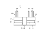
- One of two adjacent semiconductor modules 2 shown in FIG. 1 is a first semiconductor module, and the other is a second semiconductor module.
- the first semiconductor module and the second semiconductor module are arranged with one side of the first semiconductor module facing one side of the second semiconductor module.
- a pin 6 is inserted into a gap formed by combining a groove 21 on the side of the first semiconductor module and a groove 21 on the side of the second semiconductor module.
- the pin 6 is inserted along the longitudinal direction of these grooves 21.
- the first semiconductor module and the second semiconductor module are connected to each other by the pin 6 inserted into the gap formed by combining the groove 21 of the first semiconductor module and the groove 21 of the second semiconductor module.
- a part of the pin 6 is inserted into the groove 21 of the first semiconductor module, and another part of the pin 6 is inserted into the groove 21 of the second semiconductor module.
- the cross section of the part of the pin 6 inserted into the groove 21 of the first semiconductor module and the cross section of the part of the pin 6 inserted into the groove 21 of the second semiconductor module each have a trapezoidal shape that can be fitted into the groove 21.
- the pin 6 does not come out of the groove 21, and therefore the first semiconductor module and the second semiconductor module are not separated. In this way, the first semiconductor module and the second semiconductor module are connected to each other by the pin 6.
- the first semiconductor module and the second semiconductor module are integrated together using pins 6.
- the pin 6 is inserted into the groove 21 on the side of the first semiconductor module and the groove 21 on the side of the second semiconductor module facing the side of the first semiconductor module.
- the pin 6 may be inserted into the groove 21 on the side of the first semiconductor module and the groove 21 on the side of the second semiconductor module adjacent to the side of the first semiconductor module.
- the pin 6 is arranged so as to straddle the first semiconductor module and the second semiconductor module in the direction in which the pin 6 is inserted.
- the first semiconductor module and the second semiconductor module are integrated by using the pin 6.
- the number of pins 6 used to connect the first semiconductor module and the second semiconductor module is not limited to one, and may be multiple.
- the pin 6 only needs to be inserted into the groove 21 of the first semiconductor module and the groove 21 of the second semiconductor module, and can be inserted at any position.
- the shape of the groove 21 is not limited to a trapezoidal shape.
- the groove 21 may be formed in such a way that the inserted pin 6 does not come out of the groove 21 when a force is applied to at least one of the first and second semiconductor modules in a direction that pulls the first and second semiconductor modules apart.
- the groove 21 may be L-shaped or S-shaped, and the pin 6 may have a shape that corresponds to the groove 21 so that it can be inserted into the groove 21.
- the planar shape of the base plate 13 is a square with four notches 22 formed in it. Each notch 22 is formed in the center of each side of the square.
- the screw 5 shown in FIG. 1 is passed through the notch 22 and screwed into the hole in the cooler 4.
- the base plate 13 is fastened to the cooler 4.
- the semiconductor module 2 is fixed to the cooler 4.
- a recess 23 is formed on each of the four side surfaces of the case 17.
- the recess 23 is formed on the notch 22.
- the recess 23 is recessed from the outside of the sealing portion toward the inside of the sealing portion and is formed along the normal direction.
- the cross section shown in FIG. 7 is a cross section perpendicular to the normal direction and passes through the groove 21 formed on each of the four side surfaces of the case 17.
- the shape of the recess 23 in the cross section shown in FIG. 7 is a semicircle that is slightly larger than the notch 22.
- the depth of the recess 23, which is the length recessed from the outside of the sealing portion toward the inside of the sealing portion, is set to a depth that allows the head of the screw 5 to pass through when the screw 5 is installed.
- screws 5 are attached to two locations: a notch 22 at one end in the direction in which the first semiconductor module and the second semiconductor module are arranged, and a notch 22 at the other end.
- the first semiconductor module and the second semiconductor module, which are integrated with each other by pins 6, are fixed to the cooler 4 by the two screws 5, thereby fixing the cooler 4 to the semiconductor device 1.
- the position where the screw 5 is attached is not limited to the example shown in FIG. 1.
- the number of screws 5 attached is not limited to two, but is arbitrary. It is sufficient that the screw 5 is attached to at least one of the positions where the screw 5 can be attached.
- a hole into which the screw 5 is screwed is formed at the position of the cooler 4 where the screw 5 is attached.
- FIG. 1 there are six notches 22 on the outer edge of the planar shape of the semiconductor device 1 when viewed from above.
- a screw 5 can be attached at the position of each of the six notches 22.
- a screw 5 can also be attached at the position of this hole. The screw 5 is attached at least one of these positions.
- the pin 6 When the pin 6 is inserted so as to pass through the center of the semiconductor device 1 as shown in FIG. 1, and the screw 5 is attached to the hole at the center of the semiconductor device 1, the pin 6 is inserted after the screw 5 is attached. Alternatively, the pin 6 is inserted into the groove 21 of the first semiconductor module and the groove 21 of the second semiconductor module, excluding the recess 23 through which the screw 5 is passed. This prevents the pin 6 from interfering with the attachment of the screw 5.
- the multiple semiconductor modules 2 of the semiconductor device 1 are integrated by the pins 6 and fixed to the cooler 4 by the screws 5.
- the cooler 4 can be fixed to the semiconductor device 1 with a small number of parts. This makes it possible to miniaturize the configuration including the semiconductor device 1 and the cooler 4.
- the positions of the screws 5 can be appropriately selected to fix the cooler 4.
- FIG. 3 shows the shape of the top surface of the semiconductor module 2.
- FIG. 5 shows the shape of the bottom surface of the semiconductor module 2.
- the outer edge shape of the top surface of the semiconductor module 2 and the outer edge shape of the bottom surface of the semiconductor module 2 are the same.
- the planar shapes of the outer edge shape of the top surface of the semiconductor module 2 and the outer edge shape of the bottom surface of the semiconductor module 2 are the planar shapes of the semiconductor module 2 when viewed from the normal direction.
- planar shape of the semiconductor module 2 When the planar shape of the semiconductor module 2 is rotated 90 degrees around the center of the planar shape of the semiconductor module 2, the planar shape of the semiconductor module 2 after rotation overlaps with the planar shape of the semiconductor module 2 before rotation. In other words, the planar shape of the semiconductor module 2 has four-fold symmetry. In this way, the planar shape of the semiconductor module 2 has rotational symmetry.
- the posture of the outer hull of the semiconductor module 2 does not appear to change before and after the semiconductor module 2 is rotated 90 degrees around an axis in the normal direction that passes through the center of the planar shape of the semiconductor module 2 as the rotation axis.
- the planar shape of the semiconductor module 2 is the same as the planar shape of the base plate 13, and is a square with four notches 22 formed therein. Since each notch 22 is formed at the center of each side of the square, the planar shape of the semiconductor module 2 has four-fold symmetry. In addition, the planar shape of the semiconductor module 2 has four corners, just like a square.
- the lower left corner of the semiconductor module 2 is defined as the first corner.
- the corner on the same diagonal as the first corner in the planar shape of the semiconductor module 2 is defined as the second corner.
- the second corner is defined as the upper right corner of the semiconductor module 2. That is, the first corner and the second corner are the two of the four corners that face each other across the center of the planar shape of the semiconductor module 2.
- the other two of the four corners other than the first and second corners are defined as the third and fourth corners.
- the third corner is defined as the upper left corner of the semiconductor module 2.
- the fourth corner is defined as the lower right corner of the semiconductor module 2.
- the upper left, lower left, upper right, and lower right represent positions relative to the center of the planar shape of the semiconductor module 2, and represent positions in FIG. 3.
- the multiple main electrodes 10 of the semiconductor module 2 include two gate electrodes 10a, six collector electrodes 10b, and six emitter electrodes 10c.
- the term "main electrodes 10" refers to the two gate electrodes 10a, the six collector electrodes 10b, and the six emitter electrodes 10c without distinction.
- Each of the six collector electrodes 10b is also referred to as a first main electrode.
- Each of the six emitter electrodes 10c is also referred to as a second main electrode.
- each of the multiple main electrodes 10 is soldered to the circuit pattern 15.
- Each of the multiple main electrodes 10 is electrically insulated from the base plate 13 by the insulating substrate 14. The other end of each of the multiple main electrodes 10 is exposed to the outside of the sealing portion.
- Each of the multiple main electrodes 10 penetrates the lid 18 and is drawn from inside the sealing portion to outside the sealing portion.
- Each of the multiple main electrodes 10 is drawn from inside the sealing portion in the opposite direction to the direction from the sealing portion to the base plate 13, i.e., upward.
- Each of the multiple main electrodes 10 extends in the normal direction from the surface of the sealing portion opposite the base plate 13, i.e., from the top surface of the lid 18.
- three collector electrodes 10b which are first main electrodes, are drawn out from the first corner.
- Three collector electrodes 10b which are first main electrodes, are drawn out from the second corner.
- Three emitter electrodes 10c which are second main electrodes, are drawn out from the third corner.
- Three emitter electrodes 10c which are second main electrodes, are drawn out from the fourth corner.
- two gate electrodes 10a are drawn out from positions adjacent to the three emitter electrodes 10c at the fourth corner.
- FIG. 9 is a perspective view showing the state in which the semiconductor device 1 according to the first embodiment is mounted on the substrate 3.
- FIG. 10 is a plan view of the substrate 3 on which the semiconductor device 1 according to the first embodiment is mounted.
- a plurality of holes 25 are formed in the substrate 3.
- a main electrode 10 passes through each of the plurality of holes 25.
- a plurality of electrodes 24 are also provided on the substrate 3. Each of the plurality of electrodes 24 is formed at a position where the main electrode 10 passes through.
- the plurality of electrodes 24 provided on the substrate 3 include an electrode 24a to which only the main electrode 10 of one of the two semiconductor modules 2 is connected, and an electrode 24b to which the main electrodes 10 of both of the two semiconductor modules 2 are connected.
- the electrode 24b is an electrode that electrically connects the main electrode 10 of one of the two semiconductor modules 2 to the main electrode 10 of the other semiconductor module 2.
- the term "electrode 24" refers to both the electrode 24a and the electrode 24b without distinction.
- the substrate 3 is placed over the semiconductor device 1.
- the main electrode 10, which is passed through the hole 25, is connected to the electrode 24 by soldering.
- the semiconductor device 1 is mounted on the substrate 3, as shown in FIG. 9.
- the two semiconductor modules 2 are electrically connected to each other via a circuit mounted on the substrate 3.
- each of the multiple main electrodes 10 extends in the normal direction from the upper surface of the lid 18, the main electrodes 10 can be passed through each hole 25 when the substrate 3 is placed over the semiconductor device 1. Since each main electrode 10 is directly joined to the substrate 3 by soldering, no additional elements, such as wiring or terminal blocks, are required to mount the semiconductor device 1 on the substrate 3. It is sufficient that the electrodes 24 and holes 25 are formed on the substrate 3, and no elements different from those required when a conventional power module is mounted need to be added to the substrate 3. Therefore, the semiconductor device 1 can be easily mounted on the substrate 3.
- each of the multiple main electrodes 10 and the circuit pattern 15 are electrically insulated from the base plate 13. Since each of the multiple main electrodes 10 extends upward from the upper surface of the lid 18, electrical insulation between each of the multiple main electrodes 10 and the cooler 4 can be easily ensured. This simplifies the insulation design of the semiconductor device 1.
- the two semiconductor modules 2 can be electrically connected in various arrangements with a short wiring pattern. That is, the two semiconductor modules 2 can be electrically connected with a wiring pattern with small inductance. Since the two semiconductor modules 2 can be electrically connected with a short wiring pattern, it is also easy to implement a snubber circuit or a protection circuit for noise countermeasures. The fact that the two semiconductor modules 2 can be electrically connected with a short wiring pattern is also advantageous in terms of ease of design and fewer malfunctions.
- the semiconductor device 1 is advantageous in terms of the arrangement of each of the semiconductor modules 2 with a high degree of freedom, simplification of the insulation design, simplicity of the wiring pattern, miniaturization of the circuit, and small inductance, compared to the case where a conventionally known discrete semiconductor is used.
- FIG. 11 is a diagram showing a first example of a combination pattern of the semiconductor modules 2 in the first embodiment.
- FIG. 12 is a diagram showing a second example of a combination pattern of the semiconductor modules 2 in the first embodiment.
- FIGS. 11 and 12 show the top surface of a semiconductor device 1 consisting of two semiconductor modules 2.
- the left semiconductor module 2 in each of Figures 11 and 12 is the first semiconductor module
- the right semiconductor module 2 is the second semiconductor module.
- electrode 24b is shown for reference to show the main electrode 10 of the first semiconductor module and the main electrode 10 of the second semiconductor module, which are electrically connected to each other by electrode 24b of substrate 3.
- the first example shown in FIG. 11 is an example in which the positions of the collector electrode 10b and the emitter electrode 10c in the first semiconductor module are the same as those in the second semiconductor module.
- the collector electrode 10b is disposed at the lower left and upper right of the first semiconductor module
- the emitter electrode 10c is disposed at the upper left and lower right of the first semiconductor module.
- the arrangement of the collector electrode 10b and the emitter electrode 10c in the second semiconductor module is the same as in the first semiconductor module.
- the first semiconductor module and the second semiconductor module are arranged so that the collector electrode 10b and the emitter electrode 10c, which are different main electrodes 10, are adjacent to each other.
- the collector electrode 10b in the upper right corner of the first semiconductor module and the emitter electrode 10c in the upper left corner of the second semiconductor module are connected to each other by electrode 24b.
- the first semiconductor module and the second semiconductor module are connected in series.
- the upper left, lower left, upper right, and lower right represent positions relative to the center of the planar shape of the semiconductor module 2, and represent positions in FIG. 11.
- the second semiconductor module is rotated 90 degrees clockwise from the state shown in FIG. 11.
- the positions of the collector electrode 10b and the emitter electrode 10c in the first semiconductor module in FIG. 12 are the same as those in the first semiconductor module shown in FIG. 11.
- the collector electrode 10b is disposed at the upper left and lower right of the second semiconductor module
- the emitter electrode 10c is disposed at the lower left and upper right of the second semiconductor module.
- the first semiconductor module and the second semiconductor module are disposed so that the main electrodes 10 of the same type are adjacent to each other. That is, the collector electrodes 10b of the same type of main electrodes 10 are adjacent to each other, and the emitter electrodes 10c of the same type of main electrodes 10 are adjacent to each other.
- the emitter electrode 10c at the lower right of the first semiconductor module and the emitter electrode 10c at the lower left of the second semiconductor module are connected to each other by electrode 24b.
- the first semiconductor module and the second semiconductor module are connected in parallel.
- the upper left, lower left, upper right, and lower right represent positions relative to the center of the planar shape of the semiconductor module 2, and represent positions in FIG. 12.
- the combination patterns of the semiconductor module 2 are not limited to those exemplified in FIG. 11 and FIG. 12.
- the planar shape of the semiconductor module 2 has rotational symmetry, the appearance of the outer shape of the second semiconductor module does not change before and after the second semiconductor module is rotated. Also, because the collector electrode 10b is disposed at two corners on one diagonal line and the emitter electrode 10c is disposed at two corners on the other diagonal line, the positions of the collector electrode 10b and the emitter electrode 10c in the second semiconductor module are different between Figures 11 and 12.
- the semiconductor device 1 can change the arrangement of the first main electrode and the second main electrode in each semiconductor module 2 without changing the posture of the outer hull of each semiconductor module 2. This allows the arrangement of each of the semiconductor modules 2 that are connected to each other with a high degree of freedom.
- the main electrodes 10 that are electrically connected between the semiconductor modules 2 can be selected with a high degree of freedom.
- the manner of electrical connection between the semiconductor modules 2 that are connected to each other can be selected with a high degree of freedom.
- the electrical connection between the semiconductor modules 2 can be selected arbitrarily, either in series or in parallel.
- the semiconductor device 1 may include a mixture of semiconductor modules 2 connected in series to each other and semiconductor modules 2 connected in parallel to each other.
- each main electrode 10 is electrically connected to the substrate 3 by soldering, but a method other than soldering may be used to connect each main electrode 10 to the substrate 3.
- each main electrode 10 may be electrically connected to the substrate 3 by pressing each main electrode 10 into the substrate 3.
- the sealing portion of the semiconductor module 2 includes the case 17, the lid 18, and the sealing material 19.
- the configuration of the sealing portion is not limited to that described above.
- the sealing portion may be made of molded resin, for example.
- the components provided on the upper surface of the base plate 13 are sealed by being covered with molded resin.
- the molded resin may be a transfer mold formed by transfer molding.
- the semiconductor chip provided in the semiconductor module 2 may be a semiconductor chip other than the IGBT 11 or the FWD 12.
- the semiconductor chip provided in the semiconductor module 2 may be, for example, a MOSFET (Metal Oxide Semiconductor Field Effect Transistor), a diode, a silicon carbide (SiC) device, or a gallium nitride (GaN) device.
- MOSFET Metal Oxide Semiconductor Field Effect Transistor
- the first main electrode and the second main electrode in the above description may be a source electrode and a drain electrode.
- the semiconductor chip provided in the semiconductor module 2 is a diode
- the first main electrode and the second main electrode in the above description may be an anode electrode and a cathode electrode.
- the semiconductor module 2 may be an IPM (Intelligent Power Module) in which a gate drive circuit is added to the configuration sealed in the sealing portion.
- the semiconductor device 1 is provided with two semiconductor modules 2.
- the number of semiconductor modules 2 constituting the semiconductor device 1 is arbitrary.
- the arrangement of each of the multiple semiconductor modules 2 is also arbitrary.
- the arrangement of the multiple semiconductor modules 2 may be determined according to the configuration of the electrical device in which the semiconductor device 1 is provided.
- the arrangement of the multiple semiconductor modules 2 may be determined according to the circuit system of the power conversion device in which the semiconductor device 1 is provided.
- FIG. 13 is a perspective view showing a semiconductor device 1A according to a first modified example of the first embodiment.
- FIG. 14 is a top view showing a semiconductor device 1A according to a first modified example of the first embodiment.
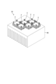
- FIG. 13 and FIG. 14 show the semiconductor device 1A and a heat sink 4A, which is a cooler. The heat sink 4A is fixed to the semiconductor device 1A.
- the semiconductor device 1A includes six semiconductor modules 2 arranged in a line to match the shape of the heat sink 4A.
- FIG. 14 an example of connection by wiring on the front side of the substrate 3 is shown by a dashed line, and an example of connection by wiring on the back side of the substrate 3 is shown by a broken line.
- the six semiconductor modules 2 include semiconductor modules 2 that are adjacent to each other and connected to each other by the substrate 3. Also, as shown in FIG. 14, among the six semiconductor modules 2, semiconductor modules 2 that are not adjacent to each other may be connected to each other by the substrate 3.
- a configuration in which multiple semiconductor modules 2 are arranged in a line like the semiconductor device 1A, can be applied to electrical equipment with a slim shape. In this way, a semiconductor device 1A can be realized in which multiple semiconductor modules 2 are arranged to match the shape desired for the electrical equipment.
- FIG. 15 is a perspective view showing a semiconductor device 1B according to a second modified example of the first embodiment.
- FIG. 16 is a top view showing a semiconductor device 1B according to a second modified example of the first embodiment.
- FIGS. 15 and 16 show the semiconductor device 1B and a heat sink 4B, which is a cooler. The heat sink 4B is fixed to the semiconductor device 1B.
- the semiconductor device 1B has three sets of two semiconductor modules 2 similar to those shown in FIG. 1. That is, the semiconductor device 1B has six semiconductor modules 2. The six semiconductor modules 2 are arranged in a staggered arrangement. In FIG. 16, an example of connection by wiring on the substrate 3 is shown by dashed lines.
- FIG. 17 is a perspective view showing a semiconductor device 1C according to a third modified example of the first embodiment.
- FIG. 17 shows the semiconductor device 1C and a heat sink 4C, which is a cooler.
- the heat sink 4C is fixed to the semiconductor device 1C.
- the semiconductor device 1C includes three sets of two semiconductor modules 2 similar to those shown in FIG. 1. That is, the semiconductor device 1C includes six semiconductor modules 2.
- the six semiconductor modules 2 are arranged in a matrix.
- the multiple semiconductor modules 2 of the semiconductor device 1 may be arranged in a staggered arrangement as shown in Figures 15 and 16, or may be arranged in a matrix as shown in Figure 17.
- the multiple semiconductor modules 2 of the semiconductor device 1 may include a mixture of semiconductor modules 2 arranged in a staggered arrangement and semiconductor modules 2 arranged in a matrix.
- FIG. 18 is a perspective view showing a semiconductor device 1D according to a fourth modified example of the first embodiment.
- FIG. 18 shows the semiconductor device 1D and a heat sink 4D, which is a cooler.
- the heat sink 4D is fixed to the semiconductor device 1D.
- the semiconductor device 1D includes six semiconductor modules 2.
- the heat sink 4D has an L-shaped planar shape.
- the six semiconductor modules 2 are arranged in an L-shape to match the planar shape of the heat sink 4D.
- the arrangement of multiple semiconductor modules 2, as in the semiconductor device 1D may be determined to match the shape of an electrical device intended by a designer. In this way, a semiconductor device 1D can be realized in which multiple semiconductor modules 2 are arranged to match the shape desired for the electrical device.
- FIG. 19 is a perspective view showing a semiconductor device 1E according to a fifth modified example of the first embodiment.
- FIG. 19 shows the semiconductor device 1E and a heat sink 4E, which is a cooler.
- the heat sink 4E is fixed to the semiconductor device 1E.
- the semiconductor device 1E includes six semiconductor modules 2.
- the six semiconductor modules 2 are arranged to match the planar shape of the heat sink 4E.
- the arrangement of the six semiconductor modules 2 in FIG. 19 is a further modification of the arrangement shown in FIG. 17 or the arrangement shown in FIG. 18.
- the arrangement of multiple semiconductor modules 2, as in semiconductor device 1E may be determined to match the shape of the electrical device intended by the designer. In this way, it is possible to realize semiconductor device 1E in which multiple semiconductor modules 2 are arranged to match the desired shape of the electrical device.
- the semiconductor device 1A-1E As in each of the modified examples of the first embodiment, by arranging multiple semiconductor modules 2, it is possible to realize a semiconductor device 1A-1E having a configuration that meets the designer's intentions. This makes it possible to apply the semiconductor device 1A-1E to power conversion devices of various circuit types, such as three-phase inverters, single-phase inverters, choppers, and three-level inverters. By combining multiple semiconductor modules 2, the semiconductor device 1A-1E can also realize functions equivalent to those of a power module in which multiple semiconductor chips are mounted in a single package.
- the semiconductor device 1, 1A-1E described in the first embodiment if a failure occurs in one of the multiple semiconductor modules 2, only the failed semiconductor module 2 can be replaced. Therefore, according to the first embodiment, it is possible to reduce the repair costs of the semiconductor device 1, 1A-1E.
- each of the semiconductor modules 2 included in the semiconductor device 1, 1A-1E has a planar shape that has four corners and has rotational symmetry.
- the first main electrode is drawn out at each of the first and second corners that face each other among the four corners.
- the second main electrode is drawn out at each of the third and fourth corners, which are the two corners other than the first and second corners among the four corners.
- the semiconductor module 2 having such a configuration can change the arrangement of the first and second main electrodes in the semiconductor module 2 by rotating the semiconductor module 2 without changing the posture of the outer hull of the semiconductor module 2.
- the main electrodes 10 that are electrically connected between the semiconductor modules 2 can be selected with a high degree of freedom. As a result, the effect of being able to arrange each of the multiple semiconductor modules 2 with a high degree of freedom is achieved.
- 1, 1A, 1B, 1C, 1D, 1E semiconductor device 2 semiconductor module, 3 substrate, 4 cooler, 4A, 4B, 4C, 4D, 4E heat sink, 5 screw, 6 pin, 10 main electrode, 10a gate electrode, 10b collector electrode, 10c emitter electrode, 11 IGBT, 12 FWD, 13 base plate, 14 insulating substrate, 15 circuit pattern, 16 wire, 17 case, 18 lid, 19 sealing material, 21 groove, 22 cutout, 23 recess, 24, 24a, 24b electrodes, 25 hole.
Landscapes
- Cooling Or The Like Of Semiconductors Or Solid State Devices (AREA)
- Engineering & Computer Science (AREA)
- Inverter Devices (AREA)
- Microelectronics & Electronic Packaging (AREA)
- Power Engineering (AREA)
Priority Applications (4)
| Application Number | Priority Date | Filing Date | Title |
|---|---|---|---|
| PCT/JP2023/022085 WO2024257265A1 (ja) | 2023-06-14 | 2023-06-14 | 半導体装置 |
| US19/117,409 US20260011685A1 (en) | 2023-06-14 | 2023-06-14 | Semiconductor device |
| JP2023568734A JP7433562B1 (ja) | 2023-06-14 | 2023-06-14 | 半導体装置 |
| CN202380090101.XA CN120513519A (zh) | 2023-06-14 | 2023-06-14 | 半导体装置 |
Applications Claiming Priority (1)
| Application Number | Priority Date | Filing Date | Title |
|---|---|---|---|
| PCT/JP2023/022085 WO2024257265A1 (ja) | 2023-06-14 | 2023-06-14 | 半導体装置 |
Publications (1)
| Publication Number | Publication Date |
|---|---|
| WO2024257265A1 true WO2024257265A1 (ja) | 2024-12-19 |
Family
ID=89904370
Family Applications (1)
| Application Number | Title | Priority Date | Filing Date |
|---|---|---|---|
| PCT/JP2023/022085 Ceased WO2024257265A1 (ja) | 2023-06-14 | 2023-06-14 | 半導体装置 |
Country Status (4)
| Country | Link |
|---|---|
| US (1) | US20260011685A1 (https=) |
| JP (1) | JP7433562B1 (https=) |
| CN (1) | CN120513519A (https=) |
| WO (1) | WO2024257265A1 (https=) |
Citations (2)
| Publication number | Priority date | Publication date | Assignee | Title |
|---|---|---|---|---|
| JP2001168278A (ja) * | 1999-12-09 | 2001-06-22 | Toshiba Corp | パワー半導体モジュール及び電力変換装置 |
| JP2009130163A (ja) * | 2007-11-26 | 2009-06-11 | Fuji Electric Device Technology Co Ltd | 半導体装置 |
Family Cites Families (8)
| Publication number | Priority date | Publication date | Assignee | Title |
|---|---|---|---|---|
| US6392145B1 (en) * | 2000-05-11 | 2002-05-21 | Advanced Micro Devices, Inc. | Semiconductor device including and integrated circuit housed in an array package having signal terminals arranged about centrally located power supply terminals |
| CN104584213B (zh) * | 2012-08-24 | 2018-02-13 | 三菱电机株式会社 | 半导体装置 |
| US10123443B2 (en) * | 2014-12-25 | 2018-11-06 | Fuji Electric Co., Ltd. | Semiconductor device |
| DE102017202770B4 (de) * | 2016-08-31 | 2023-06-07 | Infineon Technologies Austria Ag | Halbleiterchipgehäuse mit einem sich wiederholenden Grundflächenmuster |
| JP7151361B2 (ja) * | 2018-10-15 | 2022-10-12 | 富士電機株式会社 | 半導体装置 |
| CN216054654U (zh) * | 2021-04-14 | 2022-03-15 | 惠州市力迈电子有限公司 | 一种带有高气密性封装的功率晶体管 |
| CN218602437U (zh) * | 2022-08-26 | 2023-03-10 | 海丰宇航微电子有限公司 | 一种贴片型三极管 |
| CN115723970B (zh) * | 2022-11-21 | 2025-11-04 | 北京钧天航宇技术有限公司 | 面向低成本的模块化卫星结构装置 |
-
2023
- 2023-06-14 CN CN202380090101.XA patent/CN120513519A/zh active Pending
- 2023-06-14 US US19/117,409 patent/US20260011685A1/en active Pending
- 2023-06-14 JP JP2023568734A patent/JP7433562B1/ja active Active
- 2023-06-14 WO PCT/JP2023/022085 patent/WO2024257265A1/ja not_active Ceased
Patent Citations (2)
| Publication number | Priority date | Publication date | Assignee | Title |
|---|---|---|---|---|
| JP2001168278A (ja) * | 1999-12-09 | 2001-06-22 | Toshiba Corp | パワー半導体モジュール及び電力変換装置 |
| JP2009130163A (ja) * | 2007-11-26 | 2009-06-11 | Fuji Electric Device Technology Co Ltd | 半導体装置 |
Also Published As
| Publication number | Publication date |
|---|---|
| US20260011685A1 (en) | 2026-01-08 |
| JPWO2024257265A1 (https=) | 2024-12-19 |
| JP7433562B1 (ja) | 2024-02-19 |
| CN120513519A (zh) | 2025-08-19 |
Similar Documents
| Publication | Publication Date | Title |
|---|---|---|
| JP7163828B2 (ja) | 半導体モジュールとそれを備えた半導体装置 | |
| WO2013018343A1 (ja) | 半導体モジュール及びそれを搭載したインバータ | |
| JP2021158232A (ja) | 半導体モジュール | |
| JP2002141463A (ja) | 半導体モジュール | |
| US11195775B2 (en) | Semiconductor module, semiconductor device, and manufacturing method of semiconductor module | |
| KR20240040344A (ko) | 양면 방열 구조를 갖는 적층형 반도체 모듈 및 그 제조 방법 | |
| JP7491043B2 (ja) | 半導体モジュール | |
| CN109994441A (zh) | 具有增强的高功率密度的电子组件 | |
| TW202332357A (zh) | 功率模組 | |
| JP3741002B2 (ja) | 半導体装置の実装構造 | |
| CN113745203A (zh) | 半导体模块 | |
| JP7433562B1 (ja) | 半導体装置 | |
| JP7817095B2 (ja) | 半導体モジュールおよび電力変換装置 | |
| JP2023134143A (ja) | 半導体モジュール、半導体装置、及び車両 | |
| JP4155165B2 (ja) | パワーモジュール構造 | |
| CN114730742A (zh) | 半导体模块 | |
| JP7626293B2 (ja) | 半導体モジュール、半導体装置、及び半導体装置の製造方法 | |
| JP7570782B2 (ja) | 半導体装置および電力変換装置 | |
| US20240297100A1 (en) | Semiconductor module, semiconductor device, and vehicle | |
| US20240355713A1 (en) | Semiconductor device | |
| US20240266241A1 (en) | Semiconductor device | |
| JP2025151137A (ja) | インバータ装置 | |
| JP2024174287A (ja) | 半導体装置、及び車両 | |
| WO2024075445A1 (ja) | 半導体モジュール、半導体装置、及び車両 | |
| JP2025151134A (ja) | インバータ装置 |
Legal Events
| Date | Code | Title | Description |
|---|---|---|---|
| WWE | Wipo information: entry into national phase |
Ref document number: 2023568734 Country of ref document: JP |
|
| 121 | Ep: the epo has been informed by wipo that ep was designated in this application |
Ref document number: 23941570 Country of ref document: EP Kind code of ref document: A1 |
|
| WWE | Wipo information: entry into national phase |
Ref document number: 202380090101.X Country of ref document: CN |
|
| WWP | Wipo information: published in national office |
Ref document number: 202380090101.X Country of ref document: CN |
|
| NENP | Non-entry into the national phase |
Ref country code: DE |