WO2024252967A1 - 感光性導電組成物、それを用いた積層体、感光性導電接着剤、パターン付き基板の製造方法およびディスプレイ基板 - Google Patents
感光性導電組成物、それを用いた積層体、感光性導電接着剤、パターン付き基板の製造方法およびディスプレイ基板 Download PDFInfo
- Publication number
- WO2024252967A1 WO2024252967A1 PCT/JP2024/019343 JP2024019343W WO2024252967A1 WO 2024252967 A1 WO2024252967 A1 WO 2024252967A1 JP 2024019343 W JP2024019343 W JP 2024019343W WO 2024252967 A1 WO2024252967 A1 WO 2024252967A1
- Authority
- WO
- WIPO (PCT)
- Prior art keywords
- photosensitive conductive
- conductive composition
- substrate
- general formula
- polymer
- Prior art date
- Legal status (The legal status is an assumption and is not a legal conclusion. Google has not performed a legal analysis and makes no representation as to the accuracy of the status listed.)
- Ceased
Links
Images
Classifications
-
- G—PHYSICS
- G03—PHOTOGRAPHY; CINEMATOGRAPHY; ANALOGOUS TECHNIQUES USING WAVES OTHER THAN OPTICAL WAVES; ELECTROGRAPHY; HOLOGRAPHY
- G03F—PHOTOMECHANICAL PRODUCTION OF TEXTURED OR PATTERNED SURFACES, e.g. FOR PRINTING, FOR PROCESSING OF SEMICONDUCTOR DEVICES; MATERIALS THEREFOR; ORIGINALS THEREFOR; APPARATUS SPECIALLY ADAPTED THEREFOR
- G03F7/00—Photomechanical, e.g. photolithographic, production of textured or patterned surfaces, e.g. printing surfaces; Materials therefor, e.g. comprising photoresists; Apparatus specially adapted therefor
- G03F7/004—Photosensitive materials
- G03F7/027—Non-macromolecular photopolymerisable compounds having carbon-to-carbon double bonds, e.g. ethylenic compounds
- G03F7/032—Non-macromolecular photopolymerisable compounds having carbon-to-carbon double bonds, e.g. ethylenic compounds with binders
- G03F7/033—Non-macromolecular photopolymerisable compounds having carbon-to-carbon double bonds, e.g. ethylenic compounds with binders the binders being polymers obtained by reactions only involving carbon-to-carbon unsaturated bonds, e.g. vinyl polymers
-
- C—CHEMISTRY; METALLURGY
- C08—ORGANIC MACROMOLECULAR COMPOUNDS; THEIR PREPARATION OR CHEMICAL WORKING-UP; COMPOSITIONS BASED THEREON
- C08F—MACROMOLECULAR COMPOUNDS OBTAINED BY REACTIONS ONLY INVOLVING CARBON-TO-CARBON UNSATURATED BONDS
- C08F290/00—Macromolecular compounds obtained by polymerising monomers on to polymers modified by introduction of aliphatic unsaturated end or side groups
- C08F290/08—Macromolecular compounds obtained by polymerising monomers on to polymers modified by introduction of aliphatic unsaturated end or side groups on to polymers modified by introduction of unsaturated side groups
- C08F290/12—Polymers provided for in subclasses C08C or C08F
-
- G—PHYSICS
- G03—PHOTOGRAPHY; CINEMATOGRAPHY; ANALOGOUS TECHNIQUES USING WAVES OTHER THAN OPTICAL WAVES; ELECTROGRAPHY; HOLOGRAPHY
- G03F—PHOTOMECHANICAL PRODUCTION OF TEXTURED OR PATTERNED SURFACES, e.g. FOR PRINTING, FOR PROCESSING OF SEMICONDUCTOR DEVICES; MATERIALS THEREFOR; ORIGINALS THEREFOR; APPARATUS SPECIALLY ADAPTED THEREFOR
- G03F7/00—Photomechanical, e.g. photolithographic, production of textured or patterned surfaces, e.g. printing surfaces; Materials therefor, e.g. comprising photoresists; Apparatus specially adapted therefor
- G03F7/004—Photosensitive materials
- G03F7/038—Macromolecular compounds which are rendered insoluble or differentially wettable
-
- G—PHYSICS
- G03—PHOTOGRAPHY; CINEMATOGRAPHY; ANALOGOUS TECHNIQUES USING WAVES OTHER THAN OPTICAL WAVES; ELECTROGRAPHY; HOLOGRAPHY
- G03F—PHOTOMECHANICAL PRODUCTION OF TEXTURED OR PATTERNED SURFACES, e.g. FOR PRINTING, FOR PROCESSING OF SEMICONDUCTOR DEVICES; MATERIALS THEREFOR; ORIGINALS THEREFOR; APPARATUS SPECIALLY ADAPTED THEREFOR
- G03F7/00—Photomechanical, e.g. photolithographic, production of textured or patterned surfaces, e.g. printing surfaces; Materials therefor, e.g. comprising photoresists; Apparatus specially adapted therefor
- G03F7/20—Exposure; Apparatus therefor
-
- H—ELECTRICITY
- H05—ELECTRIC TECHNIQUES NOT OTHERWISE PROVIDED FOR
- H05K—PRINTED CIRCUITS; CASINGS OR CONSTRUCTIONAL DETAILS OF ELECTRIC APPARATUS; MANUFACTURE OF ASSEMBLAGES OF ELECTRICAL COMPONENTS
- H05K3/00—Apparatus or processes for manufacturing printed circuits
- H05K3/10—Apparatus or processes for manufacturing printed circuits in which conductive material is applied to the insulating support in such a manner as to form the desired conductive pattern
Definitions
- the present invention relates to a photosensitive conductive composition, a laminate using the same, a photosensitive conductive adhesive, a method for manufacturing a patterned substrate, and a display substrate.
- Photolithography is suitable for forming fine patterns, and as a technology for obtaining fine conductive patterns, for example, a photosensitive resin composition containing conductive particles (A), an alkali-soluble resin (B), and a hydrophobic compound (C) having at least one hydrocarbon group with 8 to 18 carbon atoms at the end, and the primary particle diameter of the conductive particles (A) is 0.7 ⁇ m or less (see, for example, Patent Document 1) has been proposed.
- JP 2017-181740 A International Publication No. 2022/030324
- compositions described in Patent Documents 1 and 2 can form fine patterns by development using a weak alkaline developer such as sodium carbonate or potassium carbonate.
- a weak alkaline developer such as sodium carbonate or potassium carbonate.
- highly concentrated strong alkaline developers such as tetramethylammonium hydroxide (hereinafter sometimes abbreviated as TMAH) and potassium hydroxide have traditionally been used as developers for insulating materials such as photoresists and photosensitive polyimides.
- TMAH tetramethylammonium hydroxide
- potassium hydroxide have traditionally been used as developers for insulating materials such as photoresists and photosensitive polyimides.
- the present invention aims to provide a photosensitive conductive composition that can form fine patterns even when developed using a strong alkaline developer.
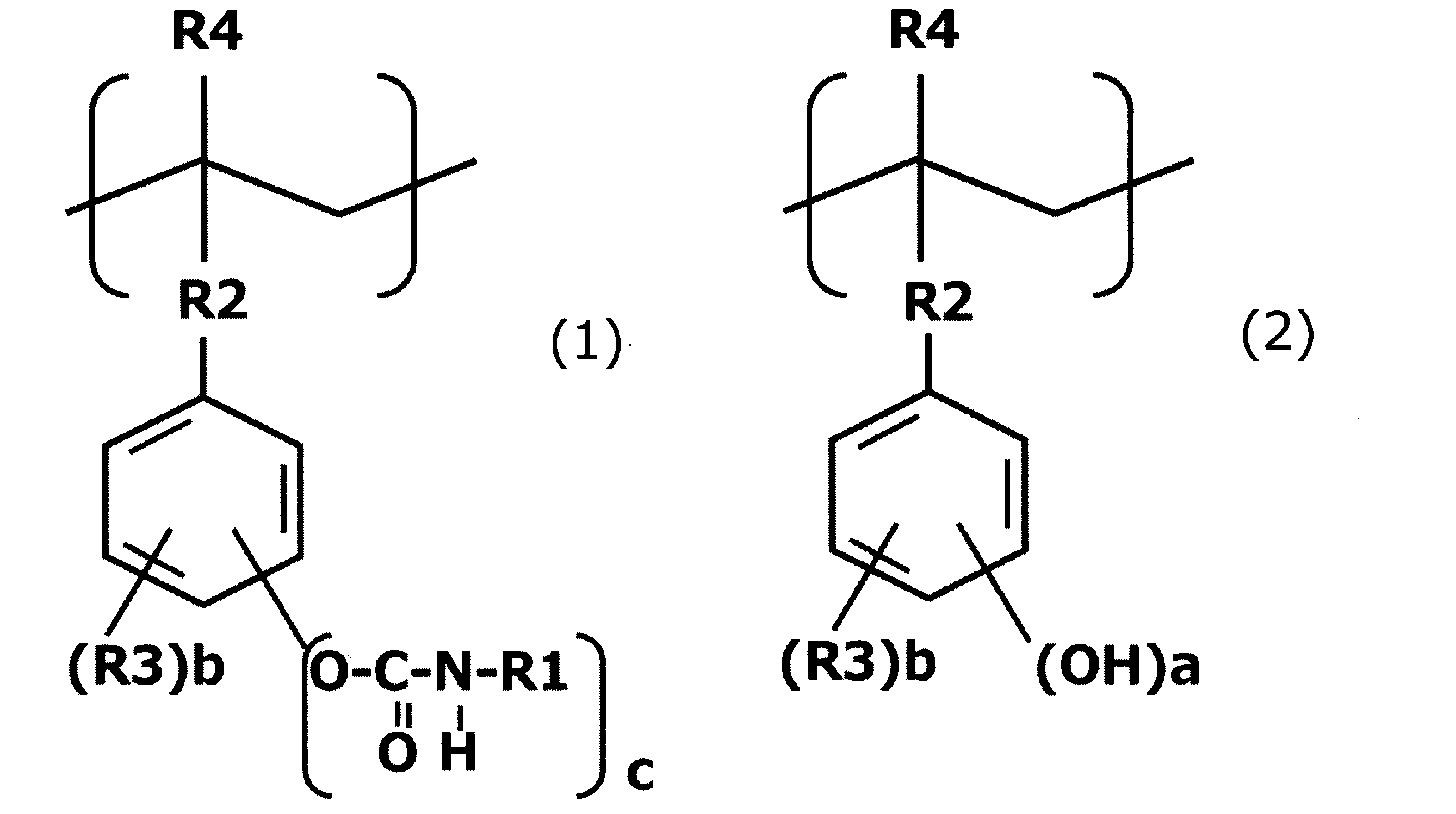
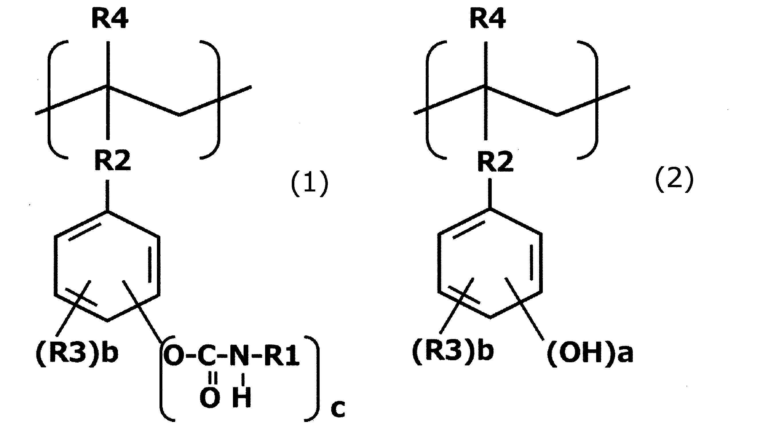
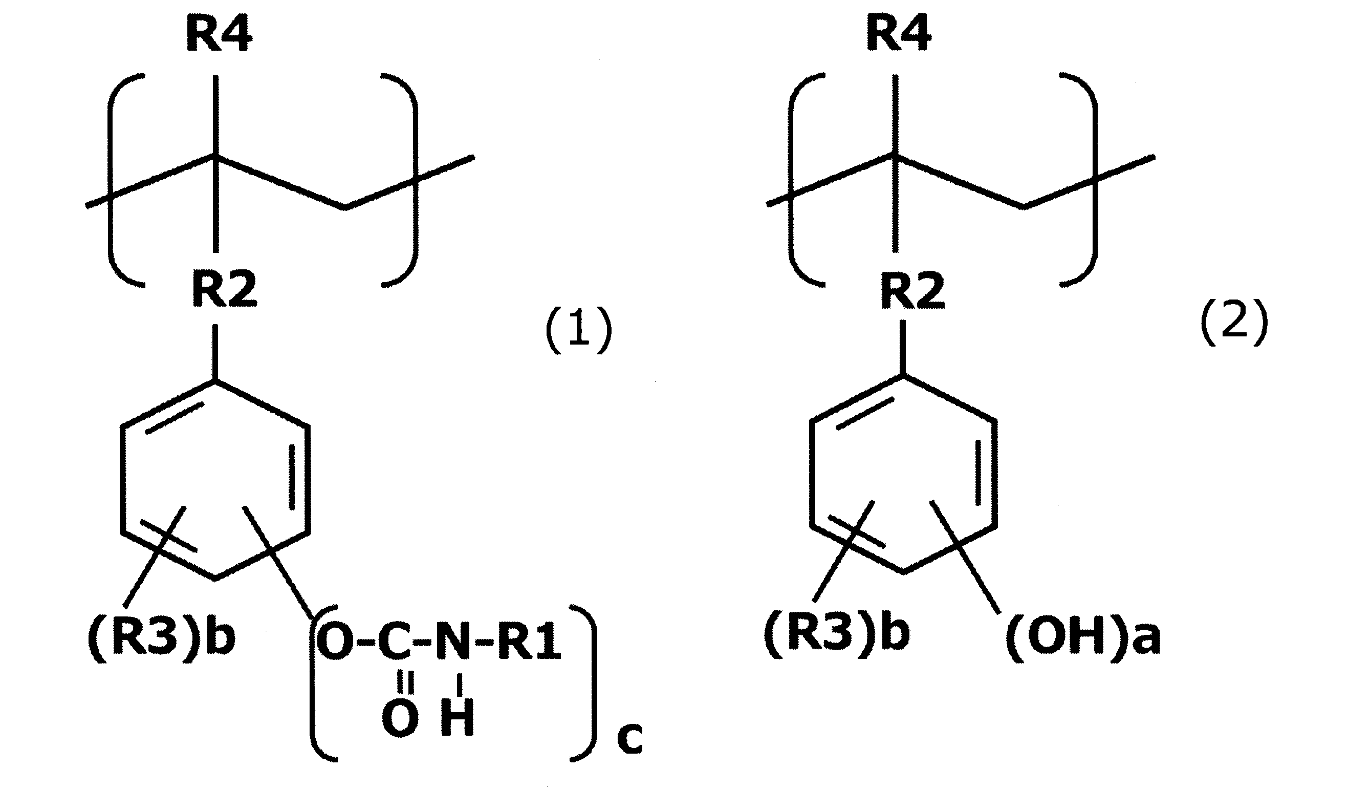
- a photosensitive conductive composition comprising a polymer (A) having a structural unit represented by the following general formula (1) and a structural unit represented by the following general formula (2), conductive particles (B), a photopolymerization initiator (C), and a photopolymerizable compound (D).
- R1 represents a monovalent group having a (meth)acryloyl group.
- R2 represents a single bond or a divalent organic group
- R3 represents an alkyl group or a halogen
- R4 represents hydrogen, an alkyl group or a halogen.
- a represents an integer of 1 to 5
- b represents an integer of 0 to 4
- c represents an integer of 1 to 5.
- a+b is 5 or less
- b+c is 5 or less.
- ⁇ 3> The photosensitive conductive composition according to ⁇ 1> or ⁇ 2>, wherein in the polymer (A), a ratio of the number of repeating structural units represented by general formula (2) to the number of repeating structural units represented by general formula (1) (general formula (2)/general formula (1)) is 0.5 to 5.
- ⁇ 4> The photosensitive conductive composition according to any one of ⁇ 1> to ⁇ 3>, further comprising a thermosetting resin (E).
- E thermosetting resin
- ⁇ 5> The photosensitive conductive composition according to any one of ⁇ 1> to ⁇ 4>, wherein the conductive particles (B) contain elemental copper.
- ⁇ 6> A laminate having a layer made of the photosensitive conductive composition according to any one of ⁇ 1> to ⁇ 5> on a release substrate.
- a photosensitive conductive adhesive comprising the photosensitive conductive composition according to any one of ⁇ 1> to ⁇ 5>.
- a method for producing a patterned substrate comprising the steps of: forming a layer made of the photosensitive conductive composition according to any one of ⁇ 1> to ⁇ 5> on a substrate; exposing the layer made of the photosensitive conductive composition to light in an imagewise manner; and developing the layer with an alkaline developer.
- the photosensitive conductive composition of the present invention can form fine patterns even by development using a strong alkaline developer.
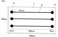
- FIG. 2 is a schematic diagram of a substrate having a resistivity measurement pattern used in the examples.
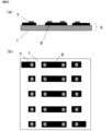
- FIG. 2 is a schematic diagram showing a mounting substrate used in the examples.
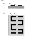
- FIG. 2 is a schematic diagram showing a silicon chip used in the examples.
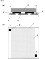
- FIG. 2 is a schematic diagram showing a silicon chip mounting substrate used in the examples.
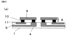
- 1 is a schematic diagram of a display substrate in which wiring and electrodes provided on the substrate are connected to LEDs.
- the photosensitive conductive composition of the present invention contains a polymer (A) (hereinafter sometimes simply referred to as polymer (A)) having a structural unit represented by the general formula (1) described below and a structural unit represented by the general formula (2) described below.
- the photosensitive conductive composition of the present invention preferably further contains a thermosetting resin (E).
- the polymer (A) functions as a binder resin that maintains the shape of the photosensitive conductive composition.
- the polymer (A) also has a function of increasing the solubility difference between the exposed and unexposed areas in development using a strong alkaline developer, due to the reduction in solubility in the developer caused by polymerization of the (meth)acryloyl group of the structural unit represented by the general formula (1) in the exposed area, and the retention of high solubility in the developer caused by the hydroxyl group of the structural unit represented by the general formula (2), making it possible to form a fine pattern.
- the photosensitive conductive composition of the present invention contains a thermosetting resin (E)
- the polymer (A) functions as a curing agent for the thermosetting resin (E) and can increase adhesion to the substrate, which is preferable.
- the polymer (A) can suppress oxidation of the metal particles and thickening of the photosensitive conductive composition due to its rust-preventing effect.
- the conductive particles (B) have the function of imparting conductivity by heat-curing or sintering the photosensitive conductive composition.
- the photopolymerization initiator (C) and the photopolymerizable compound (D) have the function of imparting photosensitivity to the conductive composition.
- the thermosetting resin (E) has the function of increasing adhesion to the substrate.
- the polymer (A) has a structural unit represented by the following general formula (1) and a structural unit represented by the following general formula (2).
- the polymer (A) may be a block copolymer or a random copolymer having these structural units, or may further have other structural units.
- R1 represents a monovalent group having a (meth)acryloyl group.
- the (meth)acryloyl group is a general term for acryloyl groups and methacryloyl groups. It is preferable that R1 has two or more (meth)acryloyl groups, which improves the crosslinking density of the exposed area and allows the formation of a finer pattern.
- c is an integer from 1 to 5. However, b+c is 5 or less. c is preferably 1, and b+c is preferably 1.
- R2 represents a single bond or a divalent organic group.
- the divalent organic group include hydrocarbon groups such as alkylene groups and alkenylene groups, carbonyl groups, ether bonds, ester bonds, urethane bonds, -NH-, -N(CH 3 )-, -N(C 2 H 5 )-, -N(C 6 H 11 ), and -N(C 6 H 5 )-.
- the hydrocarbon group may be linear, branched, or cyclic. In these groups, some of the hydrogen atoms may be substituted, and examples of the substituent include halogens.
- the number of carbon atoms in the hydrocarbon group is preferably 1 to 3. Among these, a single bond is preferable.
- R2 in general formulas (1) and (2) may be the same or different, and in each repetition of the structural unit represented by general formula (1) and the structural unit represented by general formula (2), R2 may be the same or different.
- R3 represents an alkyl group or a halogen.
- the number of carbon atoms in the alkyl group is preferably 1.
- b represents the number of substituents R3 and is an integer from 0 to 4.
- b is preferably 0.
- R3 in general formulas (1) and (2) may be the same or different, R3 in each repetition of the structural unit represented by general formula (1) and the structural unit represented by general formula (2) may be the same or different, and b in each repetition of the structural unit represented by general formula (1) may be the same or different.
- a represents an integer of 1 to 5. However, a+b is 5 or less. a is preferably 1, and a+b is preferably 1.
- R4 represents hydrogen, an alkyl group, or a halogen.
- the alkyl group preferably has 1 to 3 carbon atoms.
- the alkyl group may be linear, branched, or cyclic. Of these, hydrogen is preferred.
- the polymer (A) in the photosensitive conductive composition of the present invention can be synthesized by adding an isocyanate compound having a (meth)acryloyl group to some of the phenolic hydroxyl groups of a phenolic hydroxyl group-containing resin, such as polyparahydroxystyrene, phenolic hydroxyl group-containing acrylic copolymer, or novolac resin.
- a phenolic hydroxyl group-containing resin such as polyparahydroxystyrene, phenolic hydroxyl group-containing acrylic copolymer, or novolac resin.
- polyparahydroxystyrene include "Marukalinker” (registered trademark) M manufactured by Maruzen Petrochemical Co., Ltd. and VP Polymer manufactured by Nippon Soda Co., Ltd.
- phenolic hydroxyl group-containing acrylic copolymers examples include copolymers using phenolic hydroxyl group-containing monomers as some of the constituent components, such as NK Ester M-PHEP manufactured by Shin-Nakamura Chemical Co., Ltd., HQMA manufactured by Osaka Organic Chemical Industry Co., Ltd., HMAd manufactured by the same company, and "Shounol” (registered trademark) ARP-029P manufactured by Resonac Co., Ltd.
- novolac resins examples include WR-101, WR-102, WR-103, WR-104, PR-50, PR-100L-50P, and PR-30-40P manufactured by DIC Corporation.
- isocyanate compounds examples include Karenz (registered trademark) MOI, Karenz (registered trademark) AOI, Karenz (registered trademark) MOI-EG, Karenz (registered trademark) BEI, Karenz (registered trademark) MOI-BP, and Karenz (registered trademark) MOI-BM manufactured by Resonac Corporation.
- the ratio of the number of repeats of the structural unit represented by general formula (2) to the number of repeats of the structural unit represented by general formula (1) is preferably 0.5 to 5.
- the ratio is 0.5 or more, the solubility of the unexposed part in a strong alkaline developer is improved, the straightness of the pattern edge is increased, and a finer pattern can be formed.
- the above ratio is 5 or less, the crosslink density of the exposed part is improved, and a finer pattern can be formed.
- a thermosetting resin (E) is contained, the number of reaction points with the thermosetting resin (E) is increased, and therefore the adhesion after curing can be improved.
- the above ratio is more preferably 4.5 or less.
- the content of polymer (A) in the photosensitive conductive composition of the present invention is preferably 30 to 60% by weight of the organic solid content of the photosensitive conductive composition of the present invention, from the viewpoint of forming finer patterns.
- the conductive particles (B) refer to particles having a resistivity of 1 ⁇ cm or less.
- the conductive particles (B) include particles containing metals such as silver, gold, copper, platinum, lead, tin, nickel, aluminum, tungsten, molybdenum, chromium, titanium, indium, and palladium, alloys thereof, ITO, tin oxide, antimony-doped tin oxide, and carbon black.
- insulating particles such as resins and inorganic oxides, and conductive particles having a coating layer of the above-mentioned metals or carbon on the surface thereof are also examples of conductive particles (B). Two or more of these particles may be contained.
- the photosensitive conductive composition of the present invention uses the above-mentioned polymer (A), which suppresses oxidation and thickening and improves storage stability, even when copper particles are used as conductive particles (B).
- the photosensitive conductive composition is used for photosensitive conductive adhesive applications, it is preferable to use carbon black as the conductive particles (B) from the viewpoint of connectivity.
- the volume average particle diameter of the conductive particles (B) is preferably 0.01 ⁇ m or more from the viewpoint of dispersibility in the photosensitive conductive composition.
- the volume average particle diameter of the conductive particles (B) is preferably 3.0 ⁇ m or less, and more preferably 1.0 ⁇ m or less, from the viewpoint of forming finer patterns in the photolithography method.
- the volume average particle diameter of the conductive particles (B) can be determined by a dynamic light scattering method.
- the volume average particle diameter can be determined by irradiating a dispersion liquid containing 5 to 30 volume % of the conductive particles (B) with light having a wavelength of 780 nm using a semiconductor laser, measuring the scattered light, and then performing frequency analysis using the FFT-heterodyne method.
- the content of the conductive particles (B) in the photosensitive conductive composition of the present invention is preferably 15% by volume or more in the solid content of the photosensitive conductive composition from the viewpoint of improving the conductivity.
- the content of the conductive particles (B) is more preferably 30% by volume or more in the solid content of the photosensitive conductive composition.
- the content of the conductive particles (B) is preferably 50% by volume or less from the viewpoint of the transparency of the exposure light in the exposure process described below.
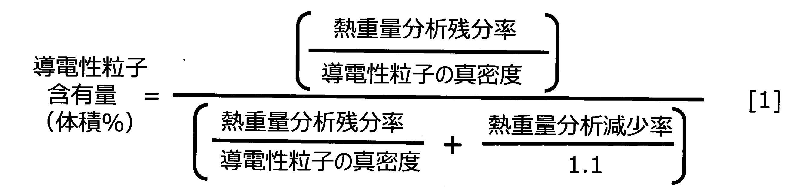
- the content of the conductive particles (B) in the photosensitive conductive composition is determined by applying the photosensitive conductive composition on a substrate, drying and removing liquid components such as a solvent, scraping off a part of the photosensitive conductive composition layer, and holding the layer at 600° C. for 1 hour in the atmosphere using a thermogravimetric analyzer to remove organic components, and determining the weight fraction of the conductive particles (B) and the weight fraction of the organic components from the ratio of the remaining weight (thermogravimetric residual fraction) and the ratio of the reduced weight (thermogravimetric reduction fraction), respectively, according to the following formula [1].
- the density of the organic component is set to 1.1 g/cm 3. However, if the composition ratio of the raw materials of the photosensitive conductive composition is known, it can be calculated from that composition ratio.
- examples of the photopolymerization initiator (C) include benzophenone derivatives, acetophenone derivatives, thioxanthone derivatives, benzyl derivatives, benzoin derivatives, oxime compounds, ⁇ -hydroxyketone compounds, ⁇ -aminoalkylphenone compounds, phosphine oxide compounds, anthrone compounds, anthraquinone compounds, etc. Two or more of these may be contained.
- the content of photopolymerization initiator (C) in the photosensitive conductive composition of the present invention is preferably 5 to 30 parts by weight per 100 parts by weight of polymer (A).
- the content of photopolymerization initiator (C) is 5 parts by weight or more, the hardening density of the exposed area increases in the exposure step described below, making it possible to form a finer pattern.
- the content of photopolymerization initiator (C) is 30 parts by weight or less, excessive light absorption in the surface layer is suppressed in the exposure step, making it possible to form a finer pattern.
- the photopolymerizable compound (D) refers to a compound having a (meth)acryloyl group and/or a maleimide skeleton.
- the photopolymerizable compound (D) include ethylene glycol di(meth)acrylate, diethylene glycol di(meth)acrylate, triethylene glycol di(meth)acrylate, 1,4-butanediol di(meth)acrylate, neopentyl glycol di(meth)acrylate, glycerin di(meth)acrylate, 2-hydroxy-3-acryloyloxypropyl (meth)acrylate, dimethylol-tricyclodecane di(meth)acrylate, and tripropylene glycol.
- Bifunctional (meth)acrylates such as di(meth)acrylate, dioxane glycol di(meth)acrylate, cyclohexane dimethanol di(meth)acrylate, tricyclodecane dimethanol di(meth)acrylate, ethoxylated (4) bisphenol A di(meth)acrylate, ethoxylated (10) bisphenol A di(meth)acrylate, a (meth)acrylic acid adduct of ethylene glycol diglycidyl ether, and a (meth)acrylic acid adduct of neopentyl glycol diglycidyl ether.
- trifunctional (meth)acrylates such as pentaerythritol tri(meth)acrylate, trimethylolpropane tri(meth)acrylate, trimethylolpropane ethoxy tri(meth)acrylate, and glycerol propoxy tri(meth)acrylate; dipentaerythritol hexa(meth)acrylate, pentaerythritol tetra(meth)acrylate, pentaerythritol ethoxy tetra(meth)acrylate, and ditrimethylolpropane tetra(meth)acrylate
- the photopolymerizable compound (D) include tetrafunctional (meth)acrylates such as EBECRYL (registered trademark) 204, EBECRYL (registered trademark) 210, EBECRYL (registered trademark) 220, EBECRYL (registered trademark) 264, EBECRYL (registered trademark)
- the content of the photopolymerizable compound (D) in the photosensitive conductive composition of the present invention is preferably 20 to 100 parts by weight per 100 parts by weight of the polymer (A).
- the content of the photopolymerizable compound (D) is 20 parts by weight or more, the hardening density of the exposed area is increased in the exposure step described below, and a finer pattern can be formed.
- the content of the photopolymerizable compound (D) is 100 parts by weight or less, excessive photopolymerization reaction is suppressed in the exposure step, and a finer pattern can be formed.
- thermosetting resin (E) examples include phenolic resin, epoxy resin, melamine resin, urea resin, and alkyd resin. Two or more of these thermosetting resins (E) may be included.
- epoxy resin is preferred, as it easily undergoes a thermosetting reaction with the polymer (A) and can further enhance adhesion.
- thermosetting resin (E) in the photosensitive conductive composition of the present invention is preferably 1 to 30 parts by weight per 100 parts by weight of polymer (A).
- the content of thermosetting resin (E) is 1 part by weight or more, the adhesion between the pattern and the substrate can be further improved.
- the content of thermosetting resin (E) is 30 parts by weight or less, the photocuring reaction proceeds smoothly in the exposure step described below, resulting in a high crosslink density, allowing the formation of a finer pattern.
- the photosensitive conductive composition of the present invention preferably further contains a solvent.
- the solvent include N,N-dimethylacetamide, N,N-dimethylformamide, N-methyl-2-pyrrolidone, dimethylimidazolidinone, dimethylsulfoxide, ⁇ -butyrolactone, ethyl lactate, 1-methoxy-2-propanol, 1-ethoxy-2-propanol, ethylene glycol mono-n-propyl ether, diacetone alcohol, tetrahydrofurfuryl alcohol, propylene glycol monomethyl ether acetate, diethylene glycol monoethyl ether acetate, diethylene glycol monomethyl ether, diethylene glycol monoethyl ether acetate, diethylene glycol monobutyl ether, diethylene glycol, and 2,2,4,-trimethyl-1,3-pentanediol monoisobutyrate.
- solvents with a boiling point of 120°C or higher are preferred,
- the photosensitive conductive composition of the present invention may contain additives such as plasticizers, leveling agents, surfactants, silane coupling agents, defoamers, and pigments, to the extent that the desired properties are not impaired.
- the photosensitive conductive composition of the present invention can be obtained by mixing the polymer (A), conductive particles (B), photopolymerization initiator (C), photopolymerizable compound (D), and, if necessary, the thermosetting resin (E), solvent and other additives.
- mixing devices include dispersing machines or kneading machines such as a triple roller, ball mill, planetary ball mill, and bead mill.
- the photosensitive conductive adhesive of the present invention is made of the photosensitive conductive composition.
- the photosensitive conductive composition exhibits electrical conductivity when heated and cured or baked, and can therefore be suitably used as a photosensitive conductive adhesive for wiring applications such as lead wiring and ITO replacement mesh wiring, and as a conductive adhesive for mounting electronic components on a circuit board.
- a so-called dry film obtained by applying the above-mentioned photosensitive conductive composition onto a release substrate and drying it as necessary can be used to form a photosensitive conductive composition layer.
- a laminate having a layer made of the photosensitive conductive composition on a release substrate is preferably used. That is, the laminate of the present invention is a laminate having a layer made of the above-mentioned photosensitive conductive composition on a release substrate.
- the layer made of the photosensitive conductive composition is preferably one from which, if the above-mentioned photosensitive conductive composition contains a liquid such as a solvent, the liquid has been removed.
- the above-mentioned laminate is intended to transfer the layer made of the photosensitive conductive composition onto a separately prepared substrate by the means described below. After transfer, the above-mentioned release substrate is separated and discarded before or after exposure. That is, the above-mentioned transfer step is one aspect of the step of forming a layer made of the above-mentioned photosensitive conductive composition in the manufacturing method of a patterned substrate of the present invention described below.
- a release substrate is a substrate that has a release layer on at least one surface.
- substrates include glass substrates and films containing resins such as polyethylene terephthalate (PET), cycloolefin polymer, polycarbonate, polyimide, aramid, fluororesin, acrylic resin, and polyurethane resin. Two or more of these may be laminated together.
- resins such as polyethylene terephthalate (PET), cycloolefin polymer, polycarbonate, polyimide, aramid, fluororesin, acrylic resin, and polyurethane resin. Two or more of these may be laminated together.
- Examples of the release agent that forms the release layer include non-silicone-based release agents and silicone-based release agents.
- non-silicone-based release agents include AL-5 manufactured by Lintec Corporation, Tesfine (registered trademark) 303, Tesfine (registered trademark) 305, and Tesfine (registered trademark) 314 manufactured by Showa Denko Materials Co., Ltd., P-OIL (registered trademark) 1010, P-OIL (registered trademark) 1050, and P-OIL (registered trademark) 1070 manufactured by Lion Specialty Chemicals Co., Ltd., and F-6711-AL, F-6758-AL, F-6441L-AL, EF-6521-AL, and F-6811-AL manufactured by AGC Seimi Chemical Co., Ltd.
- silicone-based release agents examples include "Tesfine” (registered trademark) 319 and TA31-209E manufactured by Showa Denko Materials Co., Ltd., and KS-702 and KS-707 manufactured by Shin-Etsu Chemical Co., Ltd. Among these, non-silicone-based release agents are preferred because they are less likely to cause release agent transfer.
- the thickness of the release layer is preferably 50 nm or more in order to prevent the occurrence of pinholes.
- the thickness of the release layer is preferably 1,000 nm or less in order to prevent the transfer of the release agent during the transfer process.
- Examples of methods for forming a release layer on a substrate include a method in which a release agent solution obtained by diluting the release agent with a solvent is applied onto the substrate, and the solvent is then removed.
- Examples of application methods include a coating method using a coater and a spin-coating method.
- Examples of methods for removing the solvent include heat drying.
- the peeling force of the release substrate at 25°C is preferably 100 mN/20 mm or more from the viewpoint of increasing the process window during backside transfer during storage in roll form and patterning on the release layer.
- the peeling force of the release substrate at 25°C is preferably 5,000 mN/20 mm or less from the viewpoint of widening the process window in the transfer step.
- the peeling force of the release substrate in the present invention refers to the peeling force when Nitto Denko Corporation's acrylic adhesive tape 31B is attached to the release layer-forming surface using a 2 kg roller, left to stand for 30 minutes, and then peeled under the conditions of a temperature of 25°C, a peeling angle of 180°, and a peeling speed of 0.3 m/min.
- Means for setting the peeling force within the above range include, for example, selecting one of the release agents exemplified above.
- the method for manufacturing a patterned substrate of the present invention includes a step of forming a layer made of the photosensitive conductive composition on a substrate (hereinafter, sometimes abbreviated as a photosensitive conductive composition layer forming step), a step of exposing the layer made of the photosensitive conductive composition to light in an imagewise manner (hereinafter, sometimes abbreviated as an exposure step), and a step of developing with an alkaline developer (hereinafter, sometimes abbreviated as a development step).
- a step of heat-curing the obtained pattern (hereinafter sometimes abbreviated as a curing step) or a step of baking (hereinafter sometimes abbreviated as a baking step) after the development step.
- a curing step or a step of baking (hereinafter sometimes abbreviated as a baking step) after the development step.
- the curing step or the baking step can be selected according to the composition of the photosensitive conductive composition, the heat resistance temperature of the substrate, and the desired characteristics.
- the photosensitive conductive composition layer forming process will be described.
- methods include a method in which the photosensitive conductive composition of the present invention is applied onto a substrate to form a coating film, and if the photosensitive conductive composition contains a solvent, the solvent is removed by drying to form a photosensitive conductive composition layer, and a method in which the photosensitive conductive composition layer is transferred from the aforementioned laminate onto the substrate.
- substrates include polyester films such as PET film, polyimide films, aramid films, epoxy resin substrates, polyetherimide resin substrates, polyetherketone resin, polysulfone resin substrates, glass substrates, silicon wafers, alumina substrates, aluminum nitride substrates, silicon carbide substrates, substrates with decorative layers, substrates with insulating layers, and ceramic green sheets.
- polyester films such as PET film, polyimide films, aramid films, epoxy resin substrates, polyetherimide resin substrates, polyetherketone resin, polysulfone resin substrates, glass substrates, silicon wafers, alumina substrates, aluminum nitride substrates, silicon carbide substrates, substrates with decorative layers, substrates with insulating layers, and ceramic green sheets.
- Methods for applying the photosensitive conductive composition of the present invention to a substrate include, for example, a rotary coating method using a spinner, a spray coating method, a roll coating method, a screen printing method, and a coating method using a coater such as a blade coater, a die coater, a calendar coater, a meniscus coater, or a bar coater.
- a coater such as a blade coater, a die coater, a calendar coater, a meniscus coater, or a bar coater.
- the thickness of the resulting coating film can be appropriately set based on the desired thickness of the photosensitive conductive composition layer and the total solids concentration of the photosensitive conductive composition.
- Methods for drying the coating film include, for example, heat drying using an oven, a hot plate, infrared rays, etc., and vacuum drying.
- the heating temperature is preferably 50 to 180°C, and the heating time is preferably 1 minute to several hours.
- the means for transferring the photosensitive conductive composition layer from the laminate onto the substrate includes, for example, a means for thermocompression bonding the laminate onto the substrate to transfer the photosensitive conductive composition layer.
- thermocompression devices include a laminator device and a press machine.
- the thermocompression temperature is preferably 60°C or higher from the viewpoints of suppressing the generation of voids between the substrate/photosensitive conductive composition layer, widening the process window in the development step, and forming a finer pattern.
- the thermocompression temperature is preferably 130°C or lower from the viewpoints of suppressing the thermosetting reaction of the organic components and the sintering of the conductive particles (B) and forming a finer pattern.
- the thickness of the photosensitive conductive composition layer formed in the photosensitive conductive composition layer forming step is preferably 0.5 to 50 ⁇ m.
- the thickness of the photosensitive conductive composition layer can be measured using a stylus type step gauge such as "Surfcom” (registered trademark) 1400 (manufactured by Tokyo Seimitsu Co., Ltd.). More specifically, the thickness is measured at three randomly selected locations using a stylus type step gauge under conditions of length measurement: 1 mm, scanning speed: 0.3 mm/sec, and the average value is calculated.
- Imagewise exposure may be performed through any pattern forming mask, or imagewise exposure may be performed using a direct writing exposure device.
- the light source for exposure the i-line (365 nm), h-line (405 nm), and g-line (436 nm) of a mercury lamp are preferably used.
- alkaline developers include strong alkaline aqueous solutions such as TMAH, sodium hydroxide, and potassium hydroxide, and weak alkaline aqueous solutions such as diethanolamine, diethylaminoethanol, sodium carbonate, and potassium carbonate. Since the photosensitive conductive composition of the present invention can also form a fine pattern by development using a strong alkaline developer, a strong alkaline aqueous solution is preferred as the developer, and a TMAH aqueous solution is more preferred.
- the content of the alkaline component in the alkaline developer is preferably 1% by weight or more from the viewpoint of suppressing fluctuations in development time due to carbonates generated by reaction with carbon dioxide in the air.
- alkaline developers may further contain polar solvents such as N-methyl-2-pyrrolidone, N,N-dimethylformamide, N,N-dimethylacetamide, dimethylsulfoxide, and ⁇ -butyrolactone; alcohols such as methanol, ethanol, and isopropanol; esters such as ethyl lactate and propylene glycol monomethyl ether acetate; ketones such as cyclopentanone, cyclohexanone, isobutyl ketone, and methyl isobutyl ketone; surfactants, and the like.
- polar solvents such as N-methyl-2-pyrrolidone, N,N-dimethylformamide, N,N-dimethylacetamide, dimethylsulfoxide, and ⁇ -butyrolactone
- alcohols such as methanol, ethanol, and isopropanol
- esters such as ethyl lactate and propylene glycol monomethyl ether
- Examples of development methods include spraying the developer onto the exposed film surface while the substrate is stationary or rotated, immersing the substrate in the developer, and applying ultrasonic waves while immersing the substrate in the developer.
- the pattern obtained by development may be rinsed with a rinse liquid.
- the rinse liquid include water and aqueous solutions of the aforementioned alcohols and esters.
- thermocompression devices include a thermocompression tool for a flip chip bonder and a vacuum diaphragm laminator.
- the curing process can improve the electrical conductivity by volumetric shrinkage caused by the curing of the organic components.
- the heating temperature is preferably 120°C or higher from the viewpoint of sufficiently promoting the volumetric shrinkage caused by the curing of the organic components and further improving the electrical conductivity and adhesion.
- the heating temperature is preferably 280°C or lower from the viewpoint of suppressing the thermal decomposition of the polymer (A) and further improving the adhesion.
- Curing methods include, for example, heating and drying using an oven, inert oven, or hot plate, or heating and drying using electromagnetic waves or microwaves from an ultraviolet lamp, infrared heater, halogen heater, or xenon flash lamp.
- the curing process increases the hardness of the pattern, making it possible to prevent chipping or peeling due to contact with other components. It can also improve adhesion to the substrate.
- the firing process will be described.
- the organic components are thermally decomposed and the conductive particles (B) are sintered together, thereby improving the conductivity.
- the firing temperature is preferably 600°C or higher in order to sufficiently advance the thermal decomposition of the organic components and the sintering of the conductive particles (B) with each other, thereby further improving the conductivity and adhesion.
- the firing temperature is preferably 1,000°C or lower in order to prevent breaks in the conductive particles (B) due to over-sintering.
- the firing method includes air firing, inert atmosphere firing, and reducing atmosphere firing.
- Inert atmosphere firing is a method in which firing is performed while flowing an inert gas such as nitrogen gas
- reducing atmosphere firing is a method in which firing is performed while flowing a gas with a reducing action such as hydrogen gas.
- Examples of firing equipment include a box furnace and a firing furnace. The firing conditions can be selected appropriately according to the type of conductive particles (B) and the desired characteristics.
- the display substrate of the present invention is formed by electrically connecting the wiring and/or electrodes on the substrate to LEDs by the cured product of the photosensitive conductive adhesive.
- the display substrate shown in FIG. 5 can be produced by mounting LEDs as electronic components on a substrate on which a connection pattern is formed using the photosensitive conductive adhesive of the present invention on the wiring and electrodes on the circuit board and curing the substrate.
- Specific resistance ( ⁇ cm) ⁇ resistance value ( ⁇ ) x film thickness ( ⁇ m) x line width ( ⁇ m)/line length (cm) ⁇ /100... [2].
- FIG. 3(a) is a schematic cross-sectional view of the silicon chip
- Fig. 3(b) is a schematic plan view of the silicon chip.
- This silicon chip was mounted on the mounting substrates obtained in Examples 19 to 22 and Comparative Example 3 using a bonder FC-3000 (manufactured by Toray Engineering Co., Ltd.) under conditions of a temperature of 120° C., a pressurizing pressure of 5 MPa, and a pressurizing time of 10 seconds, to produce the silicon chip mounting substrate shown in FIG. 4.
- FIG. 4(a) is a schematic cross-sectional view of the silicon chip mounting substrate
- FIG. 4(a) is a schematic cross-sectional view of the silicon chip mounting substrate
- FIG. 4(a) is a schematic cross-sectional view of the silicon chip mounting substrate
- 4(b) is a schematic plan view of the silicon chip.
- gold wiring 4 of the mounting substrate formed on glass substrate 1 and gold wiring 5 of the silicon chip formed on silicon 6 are connected by conductive pattern 2.
- the obtained silicon chip mounting substrate was heated at a temperature of 200° C. for 30 minutes using a hot air oven, and then terminal portion c point and terminal portion d point were connected with a tester to measure the resistance value and evaluate the conductivity.
- the substrate was developed using a 2.38% by weight aqueous solution of TMAH and rinsed with ultrapure water to form a developed film on the glass substrate.
- Wafer chips cut from 0.7 mm thick silicon wafers into 2 mm squares, were placed on the developed film and mounted using a vacuum diaphragm laminator MVLP500/600 (manufactured by Meiki Shisakusho Co., Ltd.) at a temperature of 120°C, a pressure of 1 MPa, and a pressure time of 10 seconds.
- the substrate was then heated at a temperature of 200°C for 30 minutes in a drying oven to obtain a sample for measuring die shear strength.
- the die shear strength of the obtained sample for measuring die shear strength was measured using a die shear strength measuring device Dage Series 4000 (manufactured by Nordson Advanced Technology Co., Ltd.) at a temperature of 25°C and a shear rate of 200 ⁇ m/sec.
- Synthesis Example 2 Polymer (A-2)
- a solution of polymer (A-2) having a solid content of 31.0 mass % was obtained in the same manner as in Synthesis Example 1, except that the amount of 1,1-(bisacryloyloxymethyl)ethyl isocyanate "Karenz” (registered trademark) BEI (manufactured by Resonac Corporation) added was changed to 7 g (29 mmol).
- Synthesis Example 3 Polymer (A-3)
- a solution of polymer (A-3) having a solid content of 46.9 mass % was obtained in the same manner as in Synthesis Example 1, except that the amount of 1,1-(bisacryloyloxymethyl)ethyl isocyanate "Karenz” (registered trademark) BEI (manufactured by Resonac Corporation) added was changed to 33 g (138 mmol).
- Ag particles Ag particles manufactured by DOWA Electronics Co., Ltd. (volume average particle size: 300 nm, specific gravity: 10 g/cm 3 , specific resistance: 1.6 ⁇ cm)
- Cu particles Cu particles manufactured by DOWA Electronics Co., Ltd. (volume average particle size: 1,000 nm, specific gravity: 9.0 g/cm 3 , 1.7 ⁇ cm)
- Carbon black particles carbon black particles manufactured by Cabot Corporation (volume average particle size: 50 nm, specific gravity: 1.9 g/cm 3 , 1.7 m ⁇ cm)
- Carbon-coated Ag particles Carbon-coated Ag particles manufactured by Nisshin Engineering Inc.
- the mixture was further dispersed using a high-pressure wet media-less atomizer "Nanomizer” (registered trademark) (Nanomizer Co., Ltd.) to obtain a volume average particle diameter of 0.15 ⁇ m and a conductive particle content of 12 A 0.0 wt % carbon black dispersion was obtained.
- a high-pressure wet media-less atomizer “Nanomizer” (registered trademark) (Nanomizer Co., Ltd.) to obtain a volume average particle diameter of 0.15 ⁇ m and a conductive particle content of 12 A 0.0 wt % carbon black dispersion was obtained.
- the mixture was further dispersed using a high-pressure wet media-less atomizer "Nanomizer” (registered trademark) (Nanomizer Co., Ltd.) to obtain a carbon-coated Ag dispersion having a volume average particle diameter of 0.2 ⁇ m and a conductive particle content of 42.5 wt %.
- anomizer registered trademark
- N-770 "EPICLON” (registered trademark) N-770; phenol novolac type epoxy resin manufactured by DIC Corporation [Release film] AL-5: Release-treated PET film (manufactured by Lintec Corporation, peel strength 1,480 mN/20 mm, film thickness 126 ⁇ m).
- Example 1 Into a 100 mL clean bottle, 20 g of the solution of polymer (A-1) obtained in Synthesis Example 1 (solid content 37.5% by mass), 1 g of the photopolymerization initiator (C) OXE-04 manufactured by BASF Japan Ltd., and 6 g of the photopolymerizable compound (D) M-315 manufactured by Toagosei Co., Ltd. were placed and mixed using a rotation-revolution vacuum mixer ARE-310 “Awatori Rentaro” (registered trademark) (manufactured by Thinky Corporation) to obtain 27 g of an organic component solution (solid content 53.7% by mass).
- ARE-310 “Awatori Rentaro” registered trademark
- the resulting 27 g organic component solution was mixed with 87.9 g of Ag particles manufactured by DOWA Electronics Co., Ltd., having a volume average particle diameter of 300 nm as conductive particles (B), and kneaded using a three-roller mill EXAKT M-50 (manufactured by EXAKT), to obtain 114.9 g of a photosensitive conductive composition (conductive particle (B) content: 40% by volume).
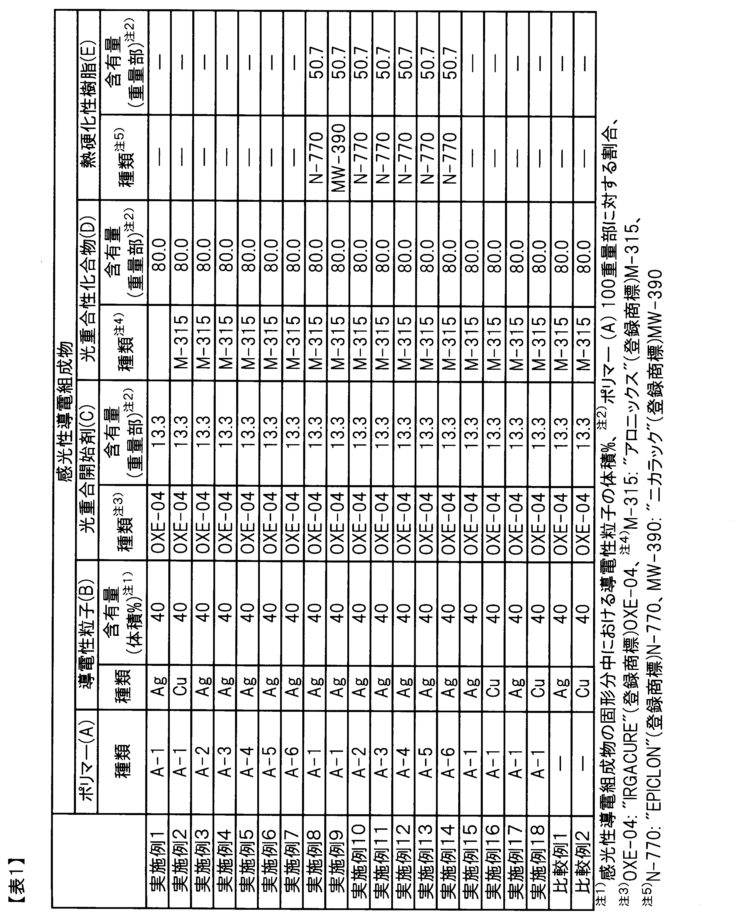
- the composition of the photosensitive conductive composition is shown in Table 1.
- the obtained photosensitive conductive composition was applied onto a glass substrate so that the film thickness after drying would be 2 ⁇ m, and then dried in a drying oven at a temperature of 100°C for 10 minutes to form a photosensitive conductive composition film with a thickness of 2 ⁇ m.
- the obtained photosensitive conductive composition film was exposed to 500 mJ/cm 2 of i-line (wavelength 365 nm) exposure using an exposure device PEM-6M (manufactured by Union Optical Co., Ltd.) having an ultra-high pressure mercury lamp through a photomask adjusted so that the obtained pattern would have seven types of lines and spaces (hereinafter abbreviated as L/S) of 20/20, 15/15, 10/10, 8/8, 7/7, 6/6 and 5/5 ⁇ m, taking into consideration the amount of line thickening in the exposed area.
- L/S seven types of lines and spaces
- the film was developed using a TMAH aqueous solution with a concentration of 2.38% by weight, rinsed with ultrapure water, and the obtained pattern was heat-cured (cured) for 30 minutes at a temperature of 200 ° C. using a hot air oven to obtain a substrate with a pattern for resolution evaluation.
- the obtained photosensitive conductive composition film was exposed to i-line (wavelength 365 nm) at an exposure dose of 500 mJ/cm 2 through a photomask using an exposure device PEM-6M (manufactured by Union Optical Co., Ltd.) having an ultra-high pressure mercury lamp. After exposure, the film was developed using a TMAH aqueous solution with a concentration of 2.38% by weight, rinsed with ultrapure water, and the obtained pattern was heat-cured at a temperature of 200° C. for 30 minutes using a hot air oven to obtain a patterned substrate for resistivity measurement shown in FIG. 1.
- FIG. 1 TMAH aqueous solution with a concentration of 2.38% by weight
- FIG. 1 shows a schematic diagram of a patterned substrate for resistivity measurement, which has a terminal portion a and a terminal portion b of ⁇ 2 mm on both ends of a conductive pattern 2 having a line width of 10 ⁇ m and a length of 200 mm on a glass substrate 1 of 180 mm ⁇ 250 mm.
- the obtained photosensitive conductive composition film was exposed to i-line (wavelength 365 nm) at an exposure dose of 500 mJ/ cm2 on the entire surface using an exposure device PEM-6M (manufactured by Union Optical Co., Ltd.) having an ultra-high pressure mercury lamp, and then heated and cured at a temperature of 200°C for 30 minutes using a hot air oven to obtain a patterned substrate for evaluating adhesion.
- PEM-6M manufactured by Union Optical Co., Ltd.
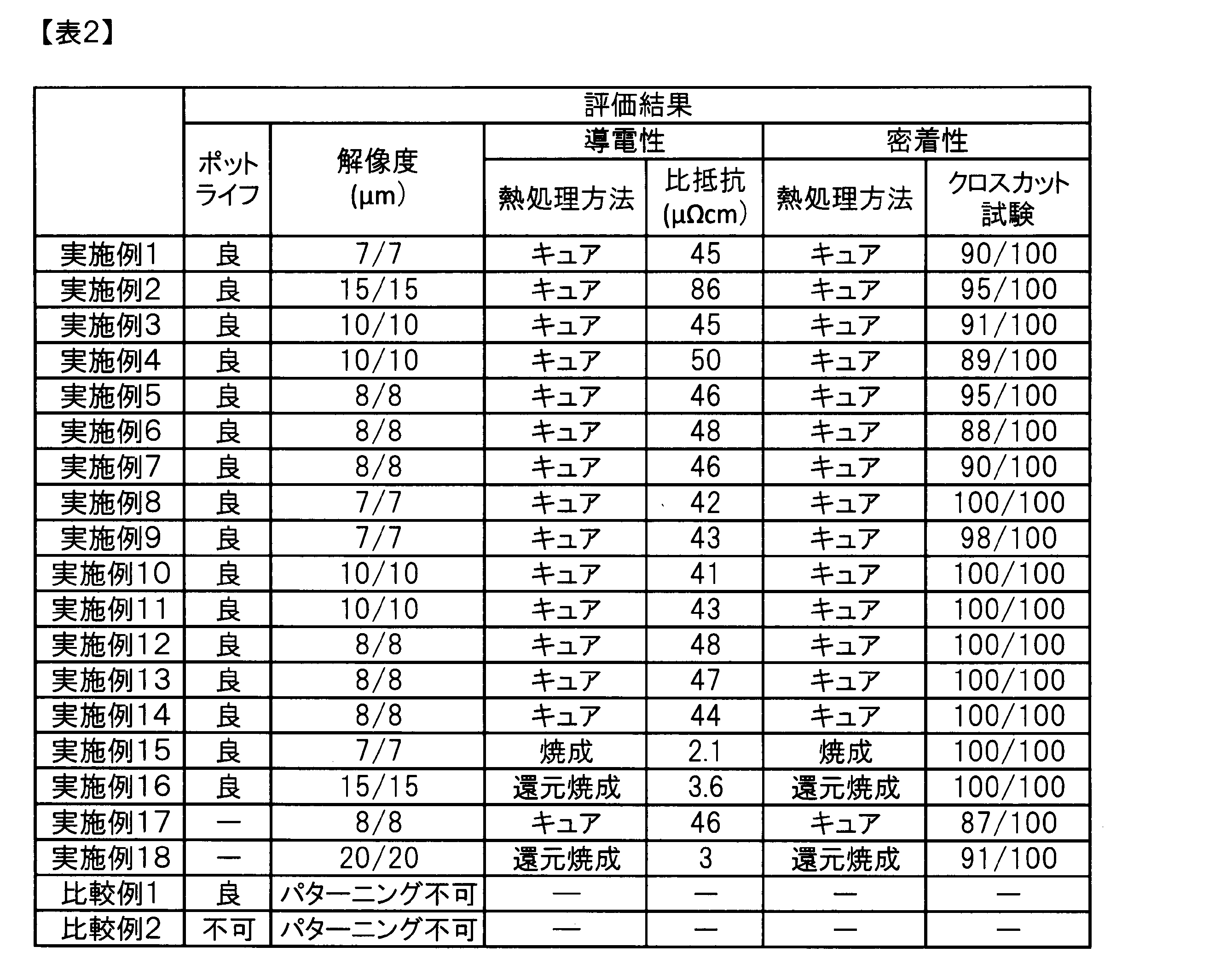
- Example 2 A photosensitive conductive composition, a patterned substrate for evaluating resolution, a patterned substrate for measuring resistivity, and a patterned substrate for evaluating adhesion were obtained in the same manner as in Example 1, except that 79.1 g of Cu particles manufactured by DOWA Electronics Co., Ltd. was used as the conductive particles (B) instead of 87.9 g of Ag particles having an average particle size of 300 nm. The results of evaluation by the above-mentioned methods are shown in Table 2.
- Examples 3 to 7 As polymer (A), solutions of polymers (A-2) to (A-6) obtained in Synthesis Examples 2 to 6 were used instead of the solution of polymer (A-1) obtained in Synthesis Example 1, and the amount of each solution added was changed so that the content of each component was as shown in Table 1.
- a photosensitive conductive composition, a substrate with a pattern for evaluating resolution, a substrate with a pattern for measuring resistivity, and a substrate with a pattern for evaluating adhesion were obtained in the same manner as in Example 1. The results of evaluation by the above-mentioned methods are shown in Table 2.
- Example 8 to 14 A photosensitive conductive composition, a patterned substrate for resolution evaluation, a patterned substrate for resistivity measurement, and a patterned substrate for adhesion evaluation were obtained in the same manner as in Example 1, except that in the production of the organic component solution, a thermosetting resin (E) shown in Table 1 was added together with the photopolymerization initiator (C) and the photopolymerizable compound (D) in an amount corresponding to the content shown in Table 1. The results of evaluation by the above-mentioned methods are shown in Table 2.
- Example 15 A photosensitive conductive composition was obtained in the same manner as in Example 1, and a photosensitive conductive composition film having a thickness of 2 ⁇ m was formed on a glass substrate.
- the obtained photosensitive conductive composition film was exposed and developed in the same manner as in Example 1, and then the obtained pattern was air-baked in a box furnace at a temperature of 800° C. for 60 minutes instead of heat-curing in a hot air oven at a temperature of 200° C. for 30 minutes.
- a substrate having a pattern for evaluating resolution, a substrate having a pattern for measuring resistivity, and a substrate having a pattern for evaluating adhesion were obtained.
- Table 2 The results of evaluation by the above-mentioned methods are shown in Table 2.
- Example 16 A substrate having a pattern for evaluating resolution, a substrate having a pattern for measuring resistivity, and a substrate having a pattern for evaluating adhesion were obtained in the same manner as in Example 15, except that a photosensitive conductive composition obtained in the same manner as in Example 2 was used instead of the photosensitive conductive composition obtained in the same manner as in Example 1, and reduction baking was performed in a reducing atmosphere of 2% by volume of hydrogen and 98% by volume of nitrogen at 800° C. for 60 minutes instead of air baking at 800° C. for 60 minutes. The results of evaluation by the above-mentioned methods are shown in Table 2.
- Example 17 The photosensitive conductive composition obtained in Example 1 was applied onto the release film AL-5 manufactured by Lintec Corporation so that the film thickness after drying would be 2 ⁇ m, and the coating was dried in a drying oven at a temperature of 100° C. for 2 minutes to obtain a laminate having a photosensitive conductive composition layer with a film thickness of 2 ⁇ m.
- the obtained laminate was thermocompressed onto a glass substrate with the photosensitive conductive composition layer facing the glass substrate under conditions of a heating temperature of 120° C., a speed of 0.2 m/min, and a pressure of 0.5 MPa to form a photosensitive conductive composition film with a film thickness of 2 ⁇ m.
- the obtained photosensitive conductive composition film was used to obtain a patterned substrate for evaluating resolution, a patterned substrate for measuring resistivity, and a patterned substrate for evaluating adhesion in the same manner as in Example 1.
- the obtained photosensitive conductive composition was in a dry film rather than a paste state, and pot life evaluation could not be performed.
- Example 18 instead of the photosensitive conductive composition obtained in Example 1, the photosensitive conductive composition obtained in Example 2 was used to form a photosensitive conductive composition film having a thickness of 2 ⁇ m on a glass substrate in the same manner as in Example 17.
- the obtained photosensitive conductive composition film was exposed and developed in the same manner as in Example 1, and then the obtained pattern was subjected to reduction baking at 800° C. for 60 minutes in a reducing atmosphere of 2% by volume of hydrogen and 98% by volume of nitrogen instead of heat curing at 200° C. for 30 minutes using a hot air oven.
- a substrate with a pattern for resolution evaluation, a substrate with a pattern for resistivity measurement, and a substrate with a pattern for adhesion evaluation were obtained in the same manner as in Example 17.
- the results of evaluation by the above-mentioned method are shown in Table 2.
- the obtained photosensitive conductive composition was in a dry film rather than a paste state, and pot life evaluation could not be performed.
- Photosensitive conductive compositions were prepared in the same manner as in Examples 1 and 2, except that 11.5 g of a PGMEA solution of a carboxyl group-containing epoxy acrylate with a solid content of 65 mass % (product name "ZCR-1797H” (manufactured by Nippon Kayaku Co., Ltd., acid value 100 mgKOH/g) was added as the polymer instead of the solution of polymer (A-1) obtained in Synthesis Example 1.
- a patterned substrate for evaluating resolution and a patterned substrate for measuring resistivity were prepared, the exposed areas were also dissolved by development, and no pattern could be formed.
- Example 19 In a 100 mL clean bottle, 20 g of the solution of polymer (A-1) obtained in Synthesis Example 1 (solid content 37.5% by mass), 1 g of the photopolymerization initiator (C)OXE-04 manufactured by BASF Japan Ltd., 6 g of the photopolymerizable compound (D)M-315 manufactured by Toagosei Co., Ltd., and 3.8 g of the thermosetting resin (E)N-770 manufactured by DIC Corporation were placed and mixed using a rotation-revolution vacuum mixer ARE-310 “Awatori Rentaro” (registered trademark) (manufactured by Thinky Corporation) to obtain 30.8 g of an organic component solution (solid content 59.4% by mass).
- ARE-310 “Awatori Rentaro” registered trademark
- the resulting 30.8 g organic component solution was mixed with 41.6 g of Ag particles manufactured by DOWA Electronics Co., Ltd., having a volume average particle diameter of 300 nm as conductive particles (B), and kneaded using a three-roller mill EXAKT M-50 (manufactured by EXAKT), to obtain 72.4 g of a photosensitive conductive composition (conductive particle (B) content: 20% by volume).
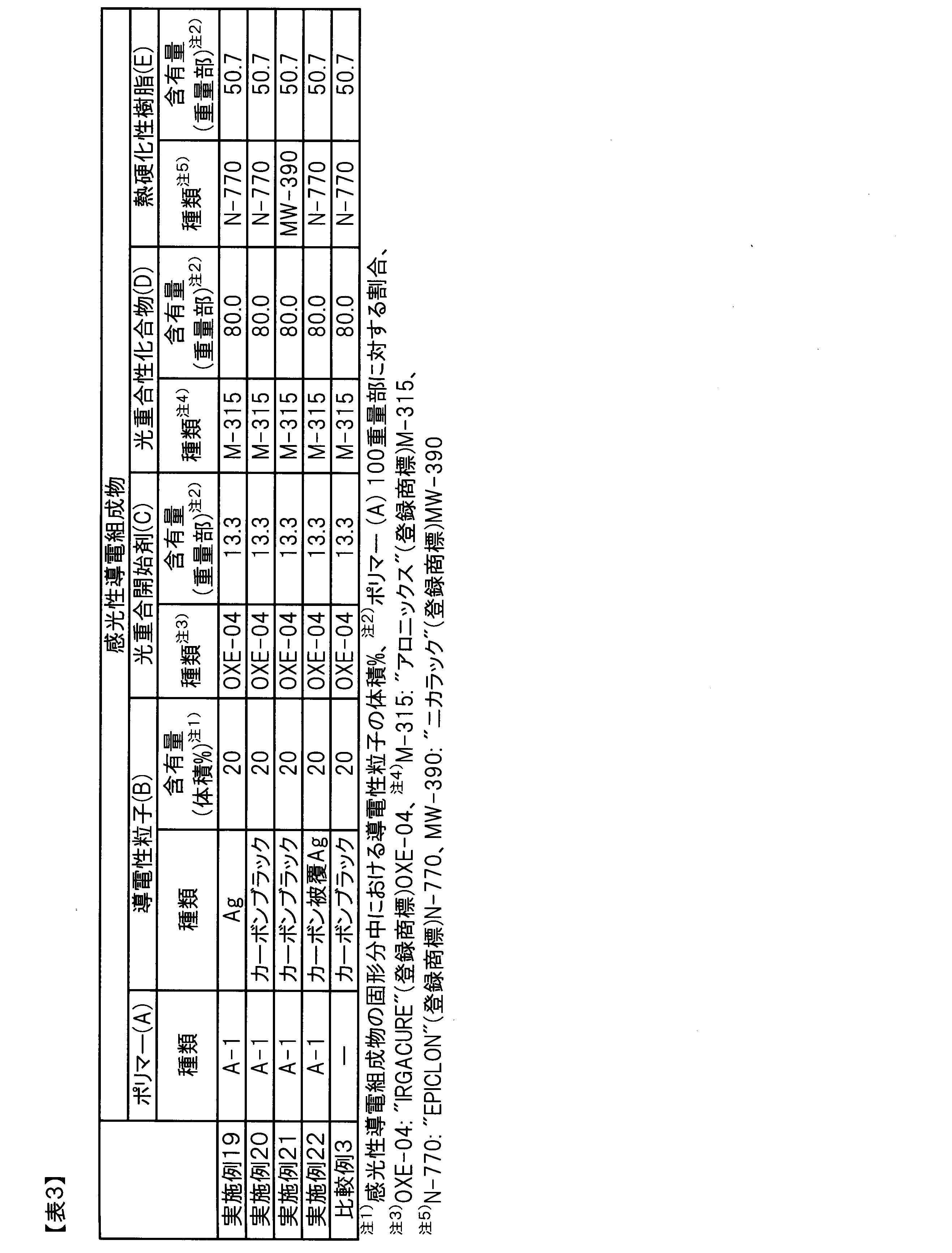
- the composition of the photosensitive conductive composition is shown in Table 3.
- the obtained photosensitive conductive composition was used to form a 2 ⁇ m-thick photosensitive conductive composition film on a glass substrate in the same manner as in Example 1.
- the obtained photosensitive conductive composition film was used to obtain a patterned substrate for resolution evaluation in the same manner as in Example 1.
- the obtained photosensitive conductive composition film was exposed to i-line (wavelength 365 nm) at an exposure dose of 500 mJ/cm2 through a photomask using an exposure device PEM-6M (manufactured by Union Optical Co., Ltd.) having an ultra-high pressure mercury lamp. After exposure, the film was developed using a TMAH aqueous solution with a concentration of 2.38% by weight, and rinsed with ultrapure water to obtain a mounting substrate as shown in FIG. 2.
- FIG. 2 (a) shows the mounting substrate
- FIG. 2(b) is a schematic plan view of the mounting substrate.
- the mounting substrate has a pre-cure pattern 7 of ⁇ 100 ⁇ m on the gold wiring 4 of a wiring formation substrate 3 having a gold wiring 4 with a line width of 2 mm on a glass substrate 1.
- Example 20 96.7 g of a photosensitive conductive composition (conductive particle (B) content 20 volume %) was obtained in the same manner as in Example 19, except that 65.9 g of a carbon black dispersion with a conductive particle content of 12.0 wt % obtained in Synthesis Example 7 was used instead of 41.6 g of Ag particles manufactured by DOWA Electronics Co., Ltd. with a volume average particle diameter of 300 nm as the conductive particles (B).
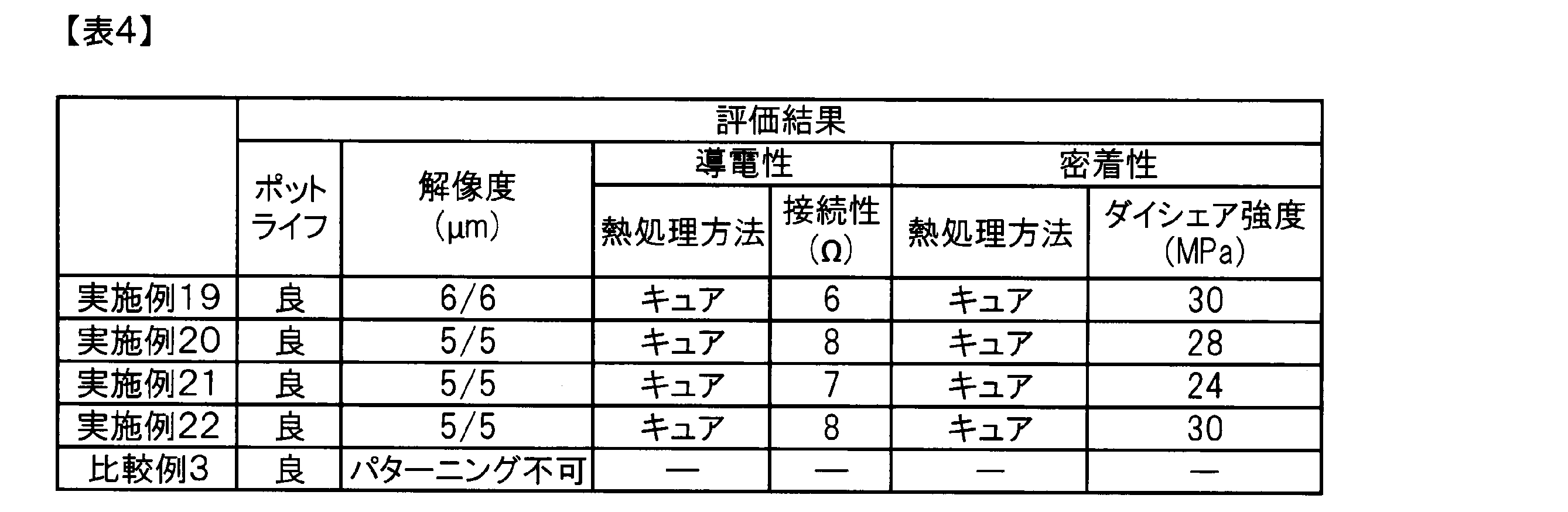
- Table 3 shows the composition of the photosensitive conductive composition. Using the obtained photosensitive conductive composition, a patterned substrate for resolution evaluation and a mounting substrate were obtained in the same manner as in Example 19. The results of evaluation by the above-mentioned method are shown in Table 4.
- Example 21 A photosensitive conductive composition, a patterned substrate for resolution evaluation, and a mounting substrate were obtained in the same manner as in Example 20, except that MW-390 manufactured by Sanwa Chemical Co., Ltd. was used as the thermosetting resin (E) instead of N-770 manufactured by DIC Corporation. The results of evaluation by the above-mentioned methods are shown in Table 4.
- Example 22 A photosensitive conductive composition, a patterned substrate for resolution evaluation, and a mounting substrate were obtained in the same manner as in Example 20, except that 93.0 g of the carbon-coated Ag particle dispersion obtained in Synthesis Example 8 was used as the conductive particles (B) instead of 65.9 g of the carbon black dispersion obtained in Synthesis Example 7. The results of evaluation by the above-mentioned methods are shown in Table 4.
- Example 3 A photosensitive conductive composition was prepared in the same manner as in Example 20, except that 11.5 g of a PGMEA solution of a carboxyl group-containing epoxy acrylate with a solid content of 65 mass % (trade name "ZCR-1797H” (manufactured by Nippon Kayaku Co., Ltd., acid value 100 mgKOH/g) was added as the polymer instead of the solution of polymer (A-1) obtained in Synthesis Example 1.
- a patterned substrate for evaluating resolution and a mounting substrate were prepared, the exposed areas were also dissolved by development, and a pattern could not be formed.
- the photosensitive conductive composition of the present invention can be used to form fine wiring and fine conductive connections using a strong alkaline developer. It can be particularly used favorably in display manufacturing and semiconductor manufacturing, which require processing using a strong alkaline developer.
Landscapes
- Physics & Mathematics (AREA)
- General Physics & Mathematics (AREA)
- Chemical & Material Sciences (AREA)
- Chemical Kinetics & Catalysis (AREA)
- Spectroscopy & Molecular Physics (AREA)
- Engineering & Computer Science (AREA)
- Health & Medical Sciences (AREA)
- Microelectronics & Electronic Packaging (AREA)
- Manufacturing & Machinery (AREA)
- Medicinal Chemistry (AREA)
- Polymers & Plastics (AREA)
- Organic Chemistry (AREA)
- Materials For Photolithography (AREA)
Abstract
Description
<1>下記一般式(1)で表される構造単位および下記一般式(2)で表される構造単位を有するポリマー(A)、導電性粒子(B)、光重合開始剤(C)および光重合性化合物(D)を含有する感光性導電組成物。
<2>前記一般式(1)におけるR1が(メタ)アクリロイル基を2つ以上有する1価の基である<1>記載の感光性導電組成物。
<3>前記ポリマー(A)において、一般式(1)で表される構造単位の繰り返し数に対する一般式(2)で表される構造単位の繰り返し数の割合(一般式(2)/一般式(1))が0.5~5である<1>または<2>記載の感光性導電組成物。
<4>さらに熱硬化性樹脂(E)を含有する<1>~<3>のいずれか記載の感光性導電組成物。
<5>前記導電性粒子(B)が銅元素を含む<1>~<4>のいずれか記載の感光性導電組成物。
<6>離型基板上に、<1>~<5>のいずれか記載の感光性導電組成物からなる層を有する積層体。
<7><1>~<5>のいずれか記載の感光性導電組成物からなる感光性導電接着剤。
<8>基板上に、<1>~<5>のいずれか記載の感光性導電組成物からなる層を形成する工程、感光性導電組成物からなる層を画像様に露光する工程およびアルカリ現像液により現像する工程を有するパターン付き基板の製造方法。
<9><7>記載の感光性導電接着剤の硬化物により基板に設けられた配線および/または基板に設けられた電極とLEDが電気的に接続されてなるディスプレイ基板。
各実施例および比較例において作製した感光性導電組成物を室温で1日静置した後、B型粘度計DVIII(ブルックフィールド社製、スピンドルNo.14)を用いて、25℃において回転数10rpmにおける粘度η1を測定した。また、感光性導電組成物を室温で1週間静置した後、同様に粘度η7を測定した。粘度変化率(%)=(η7/η1)×100を算出し、その絶対値が2未満のものを良、2を超えるものを不可と評価した。
各実施例および比較例により得られた解像度評価用パターン付き基板の導電パターンを、光学顕微鏡を用いて拡大観察した。パターン間の残渣およびパターン剥がれの認められないパターンのうちで、L/Sの値が最小となるパターンのL/Sの値を、現像可能なL/Sの値とした。
実施例1~18および比較例1~2により得られた比抵抗測定用パターン付き基板のそれぞれの端子部a点と端子部b点を抵抗計でつないで抵抗値を測定し、下記式[2]に基づいて比抵抗を算出し、導電性を評価した。
比抵抗(μΩ・cm)={抵抗値(Ω)×膜厚(μm)×線幅(μm)/ライン長(cm)}/100・・・ [2]。
図3に示す、シリコン6上に金配線5を形成した3mm角のシリコンチップを準備した。図3(a)は、シリコンチップの断面概略図であり、図3(b)は、シリコンチップの平面概略図である。このシリコンチップを、実施例19~22および比較例3により得られた実装用基板に、ボンダーFC-3000(東レエンジニアリング(株)製を用いて、温度120℃、加圧圧力5MPa、加圧時間10秒間の条件で実装して、図4に示すシリコンチップ実装基板を作製した。図4(a)は、シリコンチップ実装基板の断面概略図であり、図4(b)は、シリコンチップの平面概略図である。シリコンチップ実装基板は、ガラス基板1上に金配線4を形成した実装用基板の金配線4と、シリコン6上に金配線5を形成したシリコンチップの金配線5とが、導電パターン2により接続されている。得られたシリコンチップ実装基板を、熱風オーブンを用いて、温度200℃で30分間加熱した後、端子部c点と端子部d点をテスターでつなぎ、抵抗値を測定し、導電性を評価した。
実施例1~18および比較例1~2により得られた密着性評価用パターン付き基板の導電パターンに、カッターを用いて、1mm幅で10×10の碁盤目状に切れ目を入れ、温度85℃、湿度85%RHに設定した恒温恒湿槽SH-661(エスペック(株)製)中、240時間静置した後、サンプルを取り出し、碁盤目状の箇所にセロハンテープ(ニチバン(株)製)を貼着して剥離し、残存マス数を計数し、残存マス数/全マス数から密着性を評価した。
ガラス基板上に、実施例19~22により得られた感光性導電組成物を、乾燥後の膜厚が2μmになるように塗布した後、熱風オーブンを用いて、温度100℃で10分間加熱乾燥し、乾燥膜を形成した。その後、超高圧水銀ランプを有する露光装置PEM-6M(ユニオン光学(株)製)を用いて、ガラス基板上の乾燥膜全面に、i線(波長365nm)の露光量500mJ/cm2で露光を行った。
(合成例1:ポリマー(A-1))
撹拌装置、冷却管、温度計およびガス導入管を備えた反応容器に、プロピレングリコールモノメチルエーテルアセタート(以下、PGMEAと略記する場合がある)60gを入れ、撹拌しながらp-ヒドロキシスチレン重合物“マルカリンカー”(登録商標)M S-2P(丸善石油化学(株)製)20g(7mmol)を加え、60℃まで昇温させて60℃で3時間撹拌し、p-ヒドロキシスチレン重合物を完全に溶解させた。その後、1,1-(ビスアクリロイルオキシメチル)エチルイソシアネート“カレンズ”(登録商標)BEI((株)レゾナック製)16g(67mmol)を加え、さらに触媒としてジラウリン酸ジブチルスズ(IV)0.02gを添加し、空気雰囲気下、80℃で8時間撹拌して重合反応を行い、固形分37.5質量%のポリマー(A-1)の溶液を得た。ポリマー(A-1)は、本発明におけるポリマー(A)に該当し、一般式(1)で表される構造単位と一般式(2)で表される構造単位を、一般式(2)/一般式(1)=1.5の割合で有し、一般式(1)のR1はアクリロイル基を2つ有する。
1,1-(ビスアクリロイルオキシメチル)エチルイソシアネート“カレンズ”(登録商標)BEI((株)レゾナック製)の添加量を7g(29mmol)に変更したこと以外は合成例1と同様にして、固形分31.0質量%のポリマー(A-2)の溶液を得た。ポリマー(A-2)は、本発明におけるポリマー(A)に該当し、一般式(1)で表される構造単位と一般式(2)で表される構造単位を、一般式(2)/一般式(1)=4.7の割合で有し、一般式(1)のR1はアクリロイル基を2つ有する。
1,1-(ビスアクリロイルオキシメチル)エチルイソシアネート“カレンズ”(登録商標)BEI((株)レゾナック製)の添加量を33g(138mmol)に変更したこと以外は合成例1と同様にして、固形分46.9質量%のポリマー(A-3)の溶液を得た。ポリマー(A-3)は、本発明におけるポリマー(A)に該当し、一般式(1)で表される構造単位と一般式(2)で表される構造単位を、一般式(2)/一般式(1)=0.2の割合で有し、一般式(1)のR1はアクリロイル基を2つ有する。
1,1-(ビスアクリロイルオキシメチル)エチルイソシアネート“カレンズ”(登録商標)BEI((株)レゾナック製)16g(67mmol)にかえて、2-イソシアネートエチルアクリレート“カレンズ”(登録商標)AOI((株)レゾナック製)9.4g(67mmol)を用いたこと以外は合成例1と同様にして、固形分32.9質量%のポリマー(A-4)の溶液を得た。ポリマー(A-4)は、本発明におけるポリマー(A)に該当し、一般式(1)で表される構造単位と一般式(2)で表される構造単位を、一般式(2)/一般式(1)=1.5の割合で有し、一般式(1)のR1はアクリロイル基を1つ有する。
撹拌装置、冷却管、温度計およびガス導入管を備えた反応容器に、フェノール性水酸基含有アクリル酸エステル:商品名「NKエステルM-PHEP」(新中村化学工業(株)製)のホモポリマー25重量%PGMEA溶液80g(4.7mmol)を加え、その後、1,1-(ビスアクリロイルオキシメチル)エチルイソシアネート“カレンズ”(登録商標)BEI((株)レゾナック製)9.5g(40mmol)を加え、さらに触媒としてジラウリン酸ジブチルスズ(IV)0.2gを添加し、空気雰囲気下、80℃で8時間撹拌して重合反応を行い、固形分33.0質量%のポリマー(A-5)の溶液を得た。ポリマー(A-5)は、本発明におけるポリマー(A)に該当し、一般式(1)で表される構造単位と一般式(2)で表される構造単位を、一般式(2)/一般式(1)=1.5の割合で有し、一般式(1)のR1はアクリロイル基を2つ有する。
撹拌装置、冷却管、温度計およびガス導入管を備えた反応容器に、固形分40質量%のフェノールノボラック樹脂PGMEA溶液:商品名「WR-104」(DIC(株)製)50g(3mmol)を加え、その後、1,1-(ビスアクリロイルオキシメチル)エチルイソシアネート“カレンズ”(登録商標)BEI((株)レゾナック製)18.0g(75mmol)を加え、さらに触媒としてジラウリン酸ジブチルスズ(IV)0.2gを添加し、空気雰囲気下、80℃で8時間撹拌して重合反応を行い、固形分55.9質量%のポリマー(A-6)の溶液を得た。ポリマー(A-6)は、本発明におけるポリマー(A)に該当し、一般式(1)で表される構造単位と一般式(2)で表される構造単位を、一般式(2)/一般式(1)=1.5の割合で有し、一般式(1)のR2はアクリロイル基を2つ有する。
・Ag粒子:DOWAエレクトロニクス(株)製Ag粒子(体積平均粒子径300nm、比重10g/cm3、比抵抗1.6μΩ・cm)
・Cu粒子:DOWAエレクトロニクス(株)製Cu粒子(体積平均粒子径1,000nm、比重9.0g/cm3、1.7μΩ・cm)
・カーボンブラック粒子:Cabot社製カーボンブラック粒子(体積平均粒子径50nm、比重1.9g/cm3、1.7mΩ・cm)
・カーボン被覆Ag粒子:日清エンジニアリング(株)製カーボン被覆Ag粒子(表面炭素被覆層の平均厚み1nm、体積平均粒子径40nm、比重9.5g/cm3、3.2μΩ・cm)
(合成例7:カーボンブラック分散液)
12.0gの上記Cabot社製カーボンブラック粒子、3gの分散剤“DISPERBYK”(登録商標)21116(ビックケミー社製)、85gのPGMEAを混合し、ホモジナイザーを用いて、1,200rpm、30分間の混合処理を施した。その後、さらに、高圧湿式メディアレス微粒化装置“ナノマイザー”(登録商標)(ナノマイザー(株))を用いて分散処理し、体積平均粒子径0.15μm、導電性粒子含有量12.0重量%のカーボンブラック分散液を得た。
65gの上記日清エンジニアリング(株)製カーボン被覆Ag粒子、3gの分散剤“DISPERBYK”(登録商標)21116(ビックケミー社製)、85gのPGMEAを混合し、ホモジナイザーを用いて、1,200rpm、30分間の混合処理を施した。その後、さらに、高圧湿式メディアレス微粒化装置“ナノマイザー”(登録商標)(ナノマイザー(株))を用いて分散処理して、体積平均粒子径0.2μm、導電性粒子含有量42.5重量%のカーボン被覆Ag分散液を得た。
・OXE-04:“IRGACURE”(登録商標)OXE-04;BASFジャパン(株)製)
[光重合性化合物(D)]
・M-315:“アロニックス”(登録商標)M-315;東亜合成(株)製 3官能モノマー
[熱硬化性樹脂(E)]
・MW-390:“ニカラック”(登録商標)MW-390;(株)三和ケミカル製 メチル化メラミン樹脂
・N-770:“EPICLON”(登録商標)N-770;DIC(株)製 フェノールノボラック型エポキシ樹脂
[離型フィルム]
・AL-5:離型処理PETフィルム(リンテック(株)製、剥離力1,480mN/20mm、膜厚126μm)。
100mLクリーンボトルに、合成例1により得られたポリマー(A-1)の溶液(固形分37.5質量%)を20g、上記BASFジャパン(株)製光重合開始剤(C)OXE-04を1g、上記東亜合成(株)製光重合性化合物(D)M-315を6g入れ、自転-公転真空ミキサーARE-310“あわとり練太郎”(登録商標)((株)シンキー製)を用いて混合して、27gの有機成分溶液(固形分53.7質量%)を得た。
導電性粒子(B)として、平均粒子径300nmのAg粒子87.9gにかえて、上記DOWAエレクトロニクス(株)製Cu粒子79.1gを用いたこと以外は実施例1と同様にして感光性導電組成物、解像度評価用パターン付き基板および比抵抗測定用パターン付き基板、密着性評価用パターン付基板を得た。前述の方法により評価した結果を表2に示す。
ポリマー(A)として、合成例1により得られたポリマー(A-1)の溶液にかえて、合成例2~6により得られたポリマー(A-2)~(A-6)の溶液を、それぞれ用いて、各成分の含有量が表1に記載のとおりになるように各溶液の添加量を変更したこと以外は実施例1と同様にして感光性導電組成物、解像度評価用パターン付き基板、比抵抗測定用パターン付き基板および密着性評価用パターン付き基板を得た。前述の方法により評価した結果を表2に示す。
有機成分溶液の製造において、光重合開始剤(C)および光重合性化合物(D)とともに、表1に示す熱硬化性樹脂(E)を、表1に記載の含有量となるように添加したこと以外は実施例1と同様にして感光性導電組成物、解像度評価用パターン付き基板、比抵抗測定用パターン付き基板および密着性評価用パターン付き基板を得た。前述の方法により評価した結果を表2に示す。
実施例1と同様にして感光性導電組成物を得て、ガラス基板上に、膜厚2μmの感光性導電組成物膜を形成した。得られた感光性導電組成物膜を実施例1と同様に露光・現像した後、得られたパターンを、熱風オーブンを用いた、温度200℃で30分間の加熱硬化にかえて、ボックス炉を用いて、温度800℃で60分間大気焼成を行ったこと以外は実施例1と同様にして解像度評価用パターン付き基板、比抵抗測定用パターン付き基板および密着性評価用パターン付き基板を得た。前述の方法により評価した結果を表2に示す。
実施例1と同様にして得られた感光性導電組成物にかえて実施例2と同様にして得られた感光性導電組成物を用いて、温度800℃、60分間大気焼成にかえて、水素2体積%、窒素98体積%の還元雰囲気下で温度800℃、60分間還元焼成を行ったこと以外は実施例15と同様にして解像度評価用パターン付き基板、比抵抗測定用パターン付き基板および密着性評価用パターン付き基板を得た。前述の方法により評価した結果を表2に示す。
上記リンテック(株)製離型フィルムAL-5上に、実施例1により得られた感光性導電組成物を、乾燥後の膜厚が2μmになるように塗布し、乾燥オーブンを用いて、温度100℃で2分間乾燥し、膜厚2μmの感光性導電組成物層を有する積層体を得た。ガラス基板上に、得られた積層体を、感光性導電組成物層をガラス基板に対向させて、加熱温度120℃、速度0.2m/分、圧力0.5MPaの条件で熱圧着して膜厚2μmの感光性導電組成物膜を形成した。
実施例1により得られた感光性導電組成物にかえて、実施例2により得られた感光性導電組成物を用いて、実施例17と同様にしてガラス基板上に膜厚2μmの感光性導電組成物膜を形成した。得られた感光性導電組成物膜を実施例1と同様に露光・現像した後、得られたパターンを、熱風オーブンを用いた、温度200℃で30分間の加熱硬化にかえて、水素2体積%、窒素98体積%の還元雰囲気下、温度800℃で60分間の還元焼成を行ったこと以外は実施例17と同様にして解像度評価用パターン付き基板、比抵抗測定用パターン付き基板および密着性評価用パターン付き基板を得た。前述の方法により評価した結果を表2に示す。得られた感光性導電組成物は、ペースト状態ではなくドライフィルムとなり、ポットライフ評価を行うことができなかった。
ポリマーとして、合成例1により得られたポリマー(A-1)の溶液にかえて、固形分65質量%のカルボキシル基含有エポキシアクリレートのPGMEA溶液 商品名「ZCR-1797H」(日本化薬(株)製、酸価100mgKOH/g)を11.5g添加したこと以外はそれぞれ実施例1~2と同様にして感光性導電組成物を作製した。解像度評価用パターン付き基板、比抵抗測定用パターン付き基板を作製したところ、現像により露光部も溶解し、パターン形成できなかった。
100mLクリーンボトルに、合成例1により得られたポリマー(A-1)の溶液(固形分37.5質量%)を20g、上記BASFジャパン(株)製光重合開始剤(C)OXE-04を1g、上記東亜合成(株)製光重合性化合物(D)M-315を6g、上記DIC(株)製熱硬化性樹脂(E)N-770を3.8g入れ、自転-公転真空ミキサーARE-310“あわとり練太郎”(登録商標)((株)シンキー製)を用いて混合して、30.8gの有機成分溶液(固形分59.4質量%)を得た。
導電性粒子(B)として体積平均粒子径300nmの上記DOWAエレクトロニクス(株)製Ag粒子41.6gにかえて、合成例7により得られた導電性粒子含有量12.0重量%のカーボンブラック分散液65.9gを用いたこと以外は実施例19と同様にして、96.7gの感光性導電組成物(導電性粒子(B)含有量20体積%)を得た。表3に感光性導電組成物の組成を示す。得られた感光性導電組成物を用いて、実施例19と同様にして解像度評価用パターン付き基板および実装用基板を得た。前述の方法により評価した結果を表4に示す。
熱硬化性樹脂(E)として、上記DIC(株)製N-770にかえて、上記(株)三和ケミカル製MW-390を用いたこと以外は実施例20と同様にして感光性導電組成物、解像度評価用パターン付き基板および実装用基板を得た。前述の方法により評価した結果を表4に示す。
導電性粒子(B)として、合成例7により得られたカーボンブラック分散液65.9gにかえて、合成例8により得られたカーボン被覆Ag粒子分散液93.0gを用いたこと以外は実施例20と同様にして感光性導電組成物、解像度評価用パターン付き基板および実装用基板を得た。前述の方法により評価した結果を表4に示す。
ポリマーとして、合成例1により得られたポリマー(A-1)の溶液にかえて、固形分65質量%のカルボキシル基含有エポキシアクリレートのPGMEA溶液商品名「ZCR-1797H」(日本化薬(株)製、酸価100mgKOH/g)を11.5g添加したこと以外は実施例20と同様にして感光性導電組成物を作製した。解像度評価用パターン付き基板および実装用基板を作製したところ、現像により露光部も溶解し、パターン形成できなかった。
2:導電パターン
3:配線形成基板
4:金電極
5:金配線
6:シリコン
7:キュア前パターン
8:LED
9:LEDの発光層
10:LEDの電極
11:キュア後パターン
a:端子部
b:端子部
c:端子部
d:端子部
Claims (9)
- 下記一般式(1)で表される構造単位および下記一般式(2)で表される構造単位を有するポリマー(A)、導電性粒子(B)、光重合開始剤(C)および光重合性化合物(D)を含有する感光性導電組成物。
- 前記一般式(1)におけるR1が(メタ)アクリロイル基を2つ以上有する1価の基である請求項1記載の感光性導電組成物。
- 前記ポリマー(A)において、一般式(1)で表される構造単位の繰り返し数に対する一般式(2)で表される構造単位の繰り返し数の割合(一般式(2)/一般式(1))が0.5~5である請求項1または2記載の感光性導電組成物。
- さらに熱硬化性樹脂(E)を含有する請求項1または2記載の感光性導電組成物。
- 前記導電性粒子(B)が銅元素を含む請求項1または2記載の感光性導電組成物。
- 離型基板上に、請求項1または2記載の感光性導電組成物からなる層を有する積層体。
- 請求項1または2記載の感光性導電組成物からなる感光性導電接着剤。
- 基板上に、請求項1または2記載の感光性導電組成物からなる層を形成する工程、感光性導電組成物からなる層を画像様に露光する工程およびアルカリ現像液により現像する工程を有するパターン付き基板の製造方法。
- 請求項7記載の感光性導電接着剤の硬化物により基板に設けられた配線および/または基板に設けられた電極とLEDが電気的に接続されてなるディスプレイ基板。
Priority Applications (3)
| Application Number | Priority Date | Filing Date | Title |
|---|---|---|---|
| KR1020257026835A KR20260018774A (ko) | 2023-06-05 | 2024-05-27 | 감광성 도전 조성물, 그것을 사용한 적층체, 감광성 도전 접착제, 패턴이 형성된 기판의 제조 방법 및 디스플레이 기판 |
| CN202480016450.1A CN120813905A (zh) | 2023-06-05 | 2024-05-27 | 感光性导电组合物、使用其的层叠体、感光性导电粘接剂、带图案的基板的制造方法及显示基板 |
| JP2024534516A JPWO2024252967A1 (ja) | 2023-06-05 | 2024-05-27 |
Applications Claiming Priority (2)
| Application Number | Priority Date | Filing Date | Title |
|---|---|---|---|
| JP2023092161 | 2023-06-05 | ||
| JP2023-092161 | 2023-06-05 |
Publications (1)
| Publication Number | Publication Date |
|---|---|
| WO2024252967A1 true WO2024252967A1 (ja) | 2024-12-12 |
Family
ID=93795877
Family Applications (1)
| Application Number | Title | Priority Date | Filing Date |
|---|---|---|---|
| PCT/JP2024/019343 Ceased WO2024252967A1 (ja) | 2023-06-05 | 2024-05-27 | 感光性導電組成物、それを用いた積層体、感光性導電接着剤、パターン付き基板の製造方法およびディスプレイ基板 |
Country Status (5)
| Country | Link |
|---|---|
| JP (1) | JPWO2024252967A1 (ja) |
| KR (1) | KR20260018774A (ja) |
| CN (1) | CN120813905A (ja) |
| TW (1) | TW202501156A (ja) |
| WO (1) | WO2024252967A1 (ja) |
Citations (2)
| Publication number | Priority date | Publication date | Assignee | Title |
|---|---|---|---|---|
| JP2018120652A (ja) * | 2017-01-23 | 2018-08-02 | 東レ株式会社 | 導電パターン形成用フィルム |
| JP2021096277A (ja) * | 2019-12-13 | 2021-06-24 | 東洋インキScホールディングス株式会社 | 感光性着色組成物、カラーフィルタ、および画像表示装置 |
Family Cites Families (2)
| Publication number | Priority date | Publication date | Assignee | Title |
|---|---|---|---|---|
| JP6604251B2 (ja) | 2016-03-30 | 2019-11-13 | 東レ株式会社 | 感光性樹脂組成物、導電性パターンの製造方法、基板、タッチパネルおよびディスプレイ |
| KR102722567B1 (ko) | 2020-08-07 | 2024-10-29 | 도레이 카부시키가이샤 | 도전 페이스트, 프린트 배선판, 프린트 배선판의 제조방법, 프린트 회로판의 제조방법 |
-
2024
- 2024-05-27 WO PCT/JP2024/019343 patent/WO2024252967A1/ja not_active Ceased
- 2024-05-27 JP JP2024534516A patent/JPWO2024252967A1/ja active Pending
- 2024-05-27 CN CN202480016450.1A patent/CN120813905A/zh active Pending
- 2024-05-27 KR KR1020257026835A patent/KR20260018774A/ko active Pending
- 2024-05-30 TW TW113119924A patent/TW202501156A/zh unknown
Patent Citations (2)
| Publication number | Priority date | Publication date | Assignee | Title |
|---|---|---|---|---|
| JP2018120652A (ja) * | 2017-01-23 | 2018-08-02 | 東レ株式会社 | 導電パターン形成用フィルム |
| JP2021096277A (ja) * | 2019-12-13 | 2021-06-24 | 東洋インキScホールディングス株式会社 | 感光性着色組成物、カラーフィルタ、および画像表示装置 |
Also Published As
| Publication number | Publication date |
|---|---|
| JPWO2024252967A1 (ja) | 2024-12-12 |
| KR20260018774A (ko) | 2026-02-09 |
| TW202501156A (zh) | 2025-01-01 |
| CN120813905A (zh) | 2025-10-17 |
Similar Documents
| Publication | Publication Date | Title |
|---|---|---|
| CN104040640B (zh) | 导电浆料和导电图案的制造方法 | |
| US9085705B2 (en) | Photosensitive conductive paste and method of producing conductive pattern | |
| KR101774307B1 (ko) | 감광성 도전 페이스트 및 도전 패턴의 제조 방법 | |
| TW201139577A (en) | Photosensitive conductive paste and method for producing conductive pattern | |
| TWI809000B (zh) | 感光性導電糊及導電圖案形成用薄膜、壓力感測器、以及附配線的基板的製造方法 | |
| WO2019202889A1 (ja) | 感光性導電ペーストおよびそれを用いたパターン形成グリーンシートの製造方法 | |
| TW201423268A (zh) | 感光性導電糊及導電圖案之製造方法 | |
| KR102722567B1 (ko) | 도전 페이스트, 프린트 배선판, 프린트 배선판의 제조방법, 프린트 회로판의 제조방법 | |
| KR101788100B1 (ko) | 도전 페이스트 및 도전 패턴의 제조 방법 | |
| CN106463199B (zh) | 导电糊剂、触控面板和导电图案的制造方法 | |
| JP5533043B2 (ja) | 感光性導電ペーストおよび導電パターンの製造方法 | |
| CN105531626A (zh) | 感光性遮光糊剂和接触式传感器用层叠图案的制造方法 | |
| CN120813905A (zh) | 感光性导电组合物、使用其的层叠体、感光性导电粘接剂、带图案的基板的制造方法及显示基板 | |
| CN113412688A (zh) | 导电图案的制造方法 | |
| CN105793804A (zh) | 接触式传感器用构件的制造方法和接触式传感器用构件 | |
| JP2010113349A (ja) | 感光性樹脂組成物 | |
| JP2025165434A (ja) | 電子部品の製造方法および樹脂組成物 | |
| TWI818467B (zh) | 硬化性樹脂組成物、乾膜、硬化物及電子零件 | |
| JP6717439B1 (ja) | 積層部材 | |
| JP2025004403A (ja) | 感光性導電ペーストおよびそれを用いた導電パターン付き基板 | |
| JP2018155994A (ja) | 感光性樹脂組成物、感光性エレメント、レジストパターンの形成方法、導体回路を有する構造体の製造方法及び配線板の製造方法 | |
| JP2017181548A (ja) | 感光性樹脂組成物、それからなる感光性樹脂組成物シートならびにそれらを用いた樹脂硬化膜付基板、半導体素子接合樹脂硬化膜付基板および半導体装置の製造方法 | |
| WO2026004396A1 (ja) | 感光性樹脂組成物、感光性エレメント、プリント配線板、及びプリント配線板の製造方法 | |
| JP2019053171A (ja) | 感光性樹脂組成物、感光性エレメント、レジストパターンの形成方法、導体回路を有する構造体の製造方法及び配線板の製造方法 | |
| JP2020083947A (ja) | ペースト、それを用いた硬化膜、焼成体、電子部品とその製造方法および配線つきセラミック積層体 |
Legal Events
| Date | Code | Title | Description |
|---|---|---|---|
| WWE | Wipo information: entry into national phase |
Ref document number: 2024534516 Country of ref document: JP |
|
| 121 | Ep: the epo has been informed by wipo that ep was designated in this application |
Ref document number: 24819199 Country of ref document: EP Kind code of ref document: A1 |
|
| WWE | Wipo information: entry into national phase |
Ref document number: 202480016450.1 Country of ref document: CN |
|
| WWP | Wipo information: published in national office |
Ref document number: 202480016450.1 Country of ref document: CN |
|
| NENP | Non-entry into the national phase |
Ref country code: DE |
|
| 122 | Ep: pct application non-entry in european phase |
Ref document number: 24819199 Country of ref document: EP Kind code of ref document: A1 |